EP0112217B1 - Patronenerzeugungsvorrichtung für integrierte Schaltungen und Verfahren für ihre Anwendung - Google Patents
Patronenerzeugungsvorrichtung für integrierte Schaltungen und Verfahren für ihre Anwendung Download PDFInfo
- Publication number
- EP0112217B1 EP0112217B1 EP83402275A EP83402275A EP0112217B1 EP 0112217 B1 EP0112217 B1 EP 0112217B1 EP 83402275 A EP83402275 A EP 83402275A EP 83402275 A EP83402275 A EP 83402275A EP 0112217 B1 EP0112217 B1 EP 0112217B1
- Authority
- EP
- European Patent Office
- Prior art keywords
- patterns
- light
- reticle
- magneto
- layer
- Prior art date
- Legal status (The legal status is an assumption and is not a legal conclusion. Google has not performed a legal analysis and makes no representation as to the accuracy of the status listed.)
- Expired
Links
Images


Classifications
-
- G—PHYSICS
- G03—PHOTOGRAPHY; CINEMATOGRAPHY; ANALOGOUS TECHNIQUES USING WAVES OTHER THAN OPTICAL WAVES; ELECTROGRAPHY; HOLOGRAPHY
- G03F—PHOTOMECHANICAL PRODUCTION OF TEXTURED OR PATTERNED SURFACES, e.g. FOR PRINTING, FOR PROCESSING OF SEMICONDUCTOR DEVICES; MATERIALS THEREFOR; ORIGINALS THEREFOR; APPARATUS SPECIALLY ADAPTED THEREFOR
- G03F7/00—Photomechanical, e.g. photolithographic, production of textured or patterned surfaces, e.g. printing surfaces; Materials therefor, e.g. comprising photoresists; Apparatus specially adapted therefor
- G03F7/70—Microphotolithographic exposure; Apparatus therefor
- G03F7/70216—Mask projection systems
- G03F7/70283—Mask effects on the imaging process
- G03F7/70291—Addressable masks, e.g. spatial light modulators [SLMs], digital micro-mirror devices [DMDs] or liquid crystal display [LCD] patterning devices
Definitions
- the present invention relates to a pattern generator for integrated circuits and the method for generating patterns using this generator. It is more particularly applicable to the manufacture of circuits with very high integration (often designated by the acronym VLSI) used in the electronic circuits of information processing systems.
- VLSI very high integration
- an integrated circuit can be defined as a stack of a plurality of different layers on a silicon substrate. These various extremely thin layers can for example be made of silicon oxide, phosphosilicate glass, silicon nitride, poly silicon, semiconductors, metallic layers of aluminum.
- silicon oxide silicon oxide
- phosphosilicate glass silicon nitride
- poly silicon silicon
- semiconductors metallic layers of aluminum.
- chips physically distinct from each other.
- a silicon substrate whose dimensions are substantially those of a disc having a diameter of the order of 120 millimeters, one can make several tens of chips having for example the shape of squares of a few millimeters on a side.
- the chips are physically separated from each other, for example by sawing.
- the manufacturing process thereof comprises different stages using different techniques such as: deposition of material on the layer, etchings, doping of the layer, oxidation of the layer etc ...
- a (or more) determined geographical area on which a plurality of patterns to be represented is defined. This is done using a technique usually referred to as photolithography.
- the photolithography technique consists first of all in coating the layer of the integrated circuit that one seeks to treat with a photo-sensitive resin. This layer coated with its resin is then illuminated by an appropriate light radiation through either a mask or a reticle carrying the representation of all the patterns to be reproduced on the area to be treated of the layer of the integrated circuit that is sought. to develop. This latter operation is currently referred to as "sunstroke".
- the lighted areas of the resin undergo a chemical transformation.
- photo-sensitive resins There are two types of photo-sensitive resins, namely positive resins and negative resins.
- positive resins the areas that one seeks to treat are exposed (illuminated by light radiation), either by deposits, or by etchings, or by oxidations, etc.).
- negative resins the areas to be protected are exposed. Whatever the type of resin, the resin is dissolved in the exposed areas in an appropriate chemical bath. It is therefore clear that the parts of the material coated with resin, which have not been exposed remain protected by the resin. We can then proceed to the various appropriate physical-chemical treatments mentioned above, through this resin mask.
- the resin is illuminated through either a mask or a reticle.
- the mask is a 1-scale representation of the areas of the resin that one seeks to protect. During the exposure, the mask is placed directly in contact with the layer of the integrated circuit coated with resin.
- the reticle is a representation on a scale much greater than 1 (usually equal to 10) of the patterns to be reproduced on the area or areas to be treated of the resin-coated layer.
- the image of this reticle is then projected in reduction (the reduction ratio is equal to the inverse of the aforementioned scale, ie one tenth in the case where this scale is equal to 10) on the layer coated with resin.
- At least one reticle or mask corresponds to a given layer of a chip (very high integration integrated circuit).
- the set of means defined above is called pattern generator for integrated circuits.
- the chip-carrying substrate is placed on a table insensitive to vibrations, provided with a system making it possible to move the substrate, according to two degrees of freedom, namely along perpendicular axes OX and OY.
- This table is equipped with an extremely precise positioning system, and equipped for example of a laser interferometer,. (for example, of the type of those manufactured by the company HEWLETT PACKARD under N ° 5501 A and described in the technical notes of this manufacturer).
- the pattern generator is placed on a machine fitted with an extremely fine optical alignment system, making it possible, from special optical patterns, to obtain positioning accuracy of the chip on which one wishes to reproduce the patterns in relation to the generator, of the order of two tenths of a micron.
- a reticle is produced in the following manner.
- a layer of chromium is deposited on a glass substrate (which must be transparent to the light beam emitted by the source), which is then coated with electro-sensitive resin.
- electro-sensitive resin is strictly analogous to that of a photo-sensitive resin, except that it undergoes a chemical transformation under the action of an electron beam and no longer under the light action.
- the patterns are written by an electron beam so that the areas to be treated (those constituting the patterns) are subjected to this beam, except that if the resin is negative, the areas that the we seek to protect are subject to the electron beam.
- the electro-sensitive resin is then revealed in an appropriate chemical bath, the chromium then being attacked in the parts which are no longer protected by the resin.
- the set of steps leading to the generation of patterns on a layer for very high integration circuits constitutes a method of generating patterns on a layer for integrated circuits, the essential successive operations of which are recalled on the table in appendix I (end of the description).
- the major drawback of the pattern generator according to the prior art as well as of the generation method which uses it is therefore the method of obtaining the reticle.
- this is remedied by replacing the reticle constituted by a deposit of chromium on a glass substrate, by a magneto-optical reticle having magneto-optical properties by Faraday effect, reminders on the magneto-optical materials and on the Faraday effect being carried out below.
- the magnetic materials having magneto-optical properties there are in particular garnets based on iron, yttrium and rare earth (gadolinium, terbium ). These materials and their magneto-optical properties are for example described in the article entitled “Large stable magnetic domains •, written by GR PULLIAM, WE ROSS, B. MACNEAL and RS BAILEY, published in the journal of Applied Physics 53 (3) from March 1982 between pages 2754 to 2758. Such materials are transparent to light.
- the magneto-optical effect is based on the principle of interaction of rectilinear polarized light with the magnetic state of the garnet or of the material.
- a light is polarized in a rectilinear manner in the plane when the electric field vector (and consequently the magnetic induction vector) always keeps the same direction in the plane perpendicular to the direction of propagation of the radiation.
- the plane of polarization is defined as the plane containing the direction of propagation of the light and the electric field vector.
- a magnetic transducer is generally composed of a magnetic circuit around which a winding is arranged and which comprises an air gap.
- thermomagnetic transducer consists on the one hand, of a ponc source heat tual to locally raise the temperature of the magnetic material above its Curie point or its compensation point and on the other hand, a system creating a permanent magnetic field of sufficient intensity to orient the magnetization of the previously heated part, during its cooling.
- the reticle is illuminated with a beam of polarized light. While crossing the fields of positive magnetization (the reasons) the vector electric field of the light undergoes a rotation equal to (+ 0), while while crossing the areas of the reticle outside the field. constituting the grounds. the electric field vector of polarized light is rotated in the plane of polarization equal to ( ⁇ 0).
- a light analyzer consisting of a crystal favoring a direction of propagation of the latter, arranged so that this direction is 90 ° from the direction that occupies the electric field vector of the light transmitted when the latter has passed through a magnetic domain of negative magnetization, a light of zero intensity is collected at the output of the analyzer when the light passes through a domain of negative magnetization, then that a light of non-zero intensity is collected when the light has passed through a magnetic domain with positive magnetization (a pattern).
- This generator is characterized in that, a light polarizer being associated with the source, the reticle comprises a thin layer of magneto-optical material with magnetization perpendicular to its surface, where the patterns consist of magnetic domains of determined shape having magnetization opposite to the magnetic medium surrounding them, the image of the patterns being reproduced by a light analyzer.
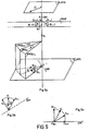
- Figure 1 represents essential constituent elements of a GMA pattern generator according to the prior art.
- the WAFA silicon substrate is placed on a TABINTA interferometric table.
- the position of each of the plates PA1 to PA6 is marked extremely precisely by an interferometric measurement system, for example equipped with a laser interferometer of the 5501A type from the company HEWLETT PACKARD.
- the identification of the chips is carried out in relation to a system of rectangular axes OX, OY.
- All the elements constituting the pattern generator on the one hand, and the silicon substrate provided with its chips PA1 to PA6 on the other hand, are aligned with respect to each other by an extremely fine optical alignment system, from special optical sights, the precision of the alignment of the chips relative to the generator being of the order of 2 tenths of a micron.
- the RETA reticle comprises a support transparent to STLA light, for example a glass substrate, on which is deposited a thin layer of COCR chromium (the description of the method of obtaining such a reticle is recalled above). It is assumed that the patterns which are drawn in Figure 2 were obtained by etching the COCR chromium layer or by etching so that a beam of light can be transmitted through them.
- FIG. 5a we consider a thin layer (a few microns to a few tens of microns thick) of a GRMF magneto-optical garnet with perpendicular magnetization, that is to say where the magnetization is normal to the surface of the layer.
- a number of small magnetic domains (a few microns to a few tens of microns) have been inscribed on this garnet, of which only three have been shown in FIG. 5a to simplify the latter. These domains are respectively the domains Di ⁇ 1, Di, Di + 1.
- the respective magnetic induction vectors of each of these domains are Bi-1, Bi, Bi + 1.
- An incident beam Fi is sent perpendicular to the surface of the garnet of rectilinear polarized light, in a direction of propagation DPi:
- the electric field of the incident beam Fi of rectilinear polarized light is Ei and in the direction indicated in FIGS. 5a, 5b and 5c, FIGS. 5a and 5b being views in space of the PPR plane, while FIG. 5c is a projection on this same.
- a plane of polarization of the light beam Fi is defined, it is defined by the direction of propagation DPi and the vector Ei (see FIG. 5a), and is called PPOLi.
- the magneto-optical garnet GRMF can transmit light. Under these conditions, when the beam of rectilinear polarized light passes through the garnet GRMF, it becomes the transmitted beam Ft.
- the beam Fi crosses a magnetic domain of negative magnetization, such as the domain Di, the beam transmitted is such that its field electric Et- rotated by an angle ( ⁇ ) with respect to the field Ei of the incident beam Fi.
- the plane of polarization of the transmitted beam Ft is then PPOLt-, the dihedral angle between this plane and the plane PPOLi also being equal to ( ⁇ ).
- the incident beam Fi crosses a magnetic domain of positive magnetization, such as for example the domain Di + 1 (Di-1) of induction Bi + 1, the transmitted beam Ft is such that its electric field Et + undergoes a rotation (+ 8) relative to the electric field Ei of the incident beam Fi.
- the plane of polarization PPOLt + then makes an angle with the plane PPOLi. dihedral equal to (+ 0).
- FIG. 5b makes it possible to better see the relative positions of the electric fields Ei, Et-, Et + of the beams Fi and Ft, according to whether Fi crosses a negative or positive magnetization domain.
- a light analyzer element In order to determine the direction of the magnetization of each of the domains Di, which amounts to determining whether the electric field vector has rotated by an angle (-0) or by an angle (+ 6), we place on the path of propagation of the transmitted beam Ft, a light analyzer element.
- This generally consists of a crystal having a preferred direction of transmission of the polarization of light, for example DPP, direction which is represented in solid lines in FIG. 5c.
- the analyzer element is placed so that this preferred direction DPP is normal to the electric field Et-.
- a light is collected whose light intensity is proportional to the square of the projection of the electric field vector on the preferred direction DPP.
- a light intensity of light proportional to the square of the module of the vector Etp- projection of the vector Et- on the direction of polarization DPP will be collected at the output of the analyzer.
- a positive magnetization domain such as Di + 1
- the main drawback of the pattern generators according to the prior art is the fact that the embodiment and control of the reticle is long and costly.
- the present invention overcomes these drawbacks by replacing the reticle of the pattern generator according to the prior art with a magneto-optical reticle constituted by the deposition of a thin magneto-optical layer with Faraday effect on a substrate transparent to light. , for example a layer of magneto-optical garnet whose properties are those which have been recalled above and illustrated by FIGS. 5a, 5b and 5c.
- All the elements of the pattern generator according to the invention GMOI on the one hand, and the TABINTII interferometric table on the other hand, are mounted in such a way that they are insensitive to vibrations.
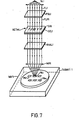
- the RETMI reticle comprises, as can be seen in FIG. 8, a magneto-optical garnet for example, with a thickness of a few microns to a few tens of microns, deposited on a substrate transparent to STLI light.
- the magneto-optical garnet GRI is magnetized perpendicular to its surface.
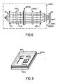
- FIG. 8 shows some patterns MOT1, MOT2, MOT3 inscribed on the magneto-optical garnet, which one seeks to reproduce on the chip PAi. It is clear that beforehand; the latter was coated with a layer of CORESI photo-sensitive resin.
- FIGS. 9 and 10 show in more detail the three patterns MOT1, MOT2 and MOT3 of the magneto-optical garnet GRI shown in FIG. 8. These three patterns are constituted by magnetic domains D1, D2, D3 having the particular shapes indicated on these same figures 9 and 10.
- the magnetization in each of the domains D1, D2, D3 is oriented upwards and is therefore assumed to be positive, while the entire surface of the GRI garnet does not constitute the domains (that is to say outside the domains D1, D2, D3) has a magnetic magnetization oriented downwards, and consequently considered as negative.
- the operation of the pattern generator according to the invention GMOI is as follows:
- the light source SLI sends a parallel light beam FLI which, through the polarizer POLI, is polarized by the latter and becomes the polarized light beam FLPI.
- This beam crosses the magneto-optical garnet and undergoes a rotation of its plane of polarization by Faraday effect equal to ( ⁇ ) if it is for example magnetic domains of negative magnetization (i.e. the surface of the GRI garnet not belonging to the magnetic domains constituting the patterns) and undergoes a rotation (+ 0) while crossing the domains where the magnetization is positive, that is to say the domains D1, D2, D3 constituting the patterns that we are trying to reproduce on the PAi chip.
- the ANALI analyzer is arranged so that at its exit, the light which crossed the negative magnetization domains has an almost null intensity, while the light transmitted by the positive magnetization domains has an intensity not null (the ratio between the intensities due respectively to the crossing of the fields of negative and positive magnetization is for example of the order of 250, as it was said above).
- the ANALI analyzer reproduces the image of patterns D1, D2, D3.
- the MPI projection means project a reduced image (most often on a 1/10 scale) of the patterns of the RETMI reticle on the CORESI resin layer.
- the CORESI resin is therefore isolated according to the images of the patterns MOT1, MOT2, MOT3 and then revealed. It is then possible to carry out on the thin layer for integrated circuits CMCII of the chip PAi the successive operations which have been described in FIGS. 4c and 4d.
- FIG. 11 represents an exemplary embodiment of a DEMI pattern writing device intended to write the patterns on a magneto-optical garnet such as GRI.
- the TMEVI magnetic transducer is preferably an integrated type magnetic transducer, similar to that described and claimed in patent application 80.07453 filed on April 2, 1980 by the Compagnie Internationale pour l'Informatique.Cll Honeywell Bull under the title "Magnetic transducer with large variable air gap for reading and writing information contained on a magnetic medium ”.
- This TMEVI transducer comprises a first pole piece PP1 and a second pole piece PP2, between which a BOBI winding is arranged.
- the pole pieces PP1 and PP2 are produced in the form of stacks of successive thin magnetic and insulating layers, while the BOBI winding is produced in the form of a stack of successive thin conductive and insulating layers.
- the two pole pieces PP1 and PP2 are magnetically coupled at their end furthest from the magneto-optical garnet GRI, and are arranged at the other end closest to this magneto-optical garnet substantially perpendicular to it to form the 'air gap.
- the transducer comprises two thin air gap layers CMME1 and CMME2, the magnetic properties of which are such that, depending on the intensity of the current that is circulated in the BOBI winding, the air gap has a large dimension varying between a minimum value GDMIN and a maximum value GDMAX.
- the pole pieces PP1 and PP2 are made of anisotropic material having a direction of easy magnetization DFA and a direction of difficult magnetization DDA.
- a current of positive intensity is sent in the BOBI winding and suitable for the width of the lines of the patterns that one seeks to trace on the CMCII layer. These patterns are recorded in the form of domains with positive magnetization.
- First operation Realization of the magneto-optical reticle by depositing a layer of magneto-optical garnet on a support transparent to light and writing patterns on the reticle by means of a magnetic transducer, or thermo-magnetic writing.
- Second operation Checking the reticle patterns using a magnetic transducer or using the magneto-optical effect.
- the reproduction and projection of the image of the reticle on the layer for an integrated circuit is carried out by means of an assembly comprising a polarized light source, a light analyzer and projection means.
Landscapes
- Physics & Mathematics (AREA)
- General Physics & Mathematics (AREA)
- Thin Magnetic Films (AREA)
- Medicines That Contain Protein Lipid Enzymes And Other Medicines (AREA)
- Pharmaceuticals Containing Other Organic And Inorganic Compounds (AREA)
Claims (6)
Applications Claiming Priority (2)
| Application Number | Priority Date | Filing Date | Title |
|---|---|---|---|
| FR8219997 | 1982-11-29 | ||
| FR8219997A FR2536872A1 (fr) | 1982-11-29 | 1982-11-29 | Generateur de motifs pour circuits integres et procede de generation de motifs utilisant ce generateur |
Publications (2)
| Publication Number | Publication Date |
|---|---|
| EP0112217A1 EP0112217A1 (de) | 1984-06-27 |
| EP0112217B1 true EP0112217B1 (de) | 1986-08-20 |
Family
ID=9279626
Family Applications (1)
| Application Number | Title | Priority Date | Filing Date |
|---|---|---|---|
| EP83402275A Expired EP0112217B1 (de) | 1982-11-29 | 1983-11-25 | Patronenerzeugungsvorrichtung für integrierte Schaltungen und Verfahren für ihre Anwendung |
Country Status (4)
| Country | Link |
|---|---|
| US (1) | US4514082A (de) |
| EP (1) | EP0112217B1 (de) |
| DE (1) | DE3365475D1 (de) |
| FR (1) | FR2536872A1 (de) |
Families Citing this family (4)
| Publication number | Priority date | Publication date | Assignee | Title |
|---|---|---|---|---|
| FR2601465B1 (fr) * | 1986-07-11 | 1988-10-21 | Bull Sa | Dispositif modulateur haute frequence de polarisation de la lumiere |
| KR950002172B1 (ko) * | 1991-06-13 | 1995-03-14 | 금성일렉트론주식회사 | 편광자를 사용한 편광노광장치 및 편광마스크 제조방법 |
| US5442184A (en) * | 1993-12-10 | 1995-08-15 | Texas Instruments Incorporated | System and method for semiconductor processing using polarized radiant energy |
| US6251550B1 (en) * | 1998-07-10 | 2001-06-26 | Ball Semiconductor, Inc. | Maskless photolithography system that digitally shifts mask data responsive to alignment data |
Family Cites Families (5)
| Publication number | Priority date | Publication date | Assignee | Title |
|---|---|---|---|---|
| FR2030468A5 (de) * | 1969-01-29 | 1970-11-13 | Thomson Brandt Csf | |
| US3909130A (en) * | 1973-08-24 | 1975-09-30 | Ilya Mikhailovich Glaskov | Microphotocomposing apparatus for making artworks |
| US4110762A (en) * | 1974-05-10 | 1978-08-29 | Commissariat A L'energie Atomique | Drawing machines especially for integrated circuit masks |
| DE2905636C2 (de) * | 1979-02-14 | 1985-06-20 | Censor Patent- Und Versuchs-Anstalt, Vaduz | Verfahren zum Kopieren von Masken auf ein Werkstück |
| JPS57176746A (en) * | 1981-04-21 | 1982-10-30 | Nippon Telegr & Teleph Corp <Ntt> | Semiconductor integrated circuit and manufacture thereof |
-
1982
- 1982-11-29 FR FR8219997A patent/FR2536872A1/fr active Granted
-
1983
- 1983-11-23 US US06/554,804 patent/US4514082A/en not_active Expired - Fee Related
- 1983-11-25 EP EP83402275A patent/EP0112217B1/de not_active Expired
- 1983-11-25 DE DE8383402275T patent/DE3365475D1/de not_active Expired
Non-Patent Citations (1)
| Title |
|---|
| IEEE TRANSACTIONS ON ELECTRON DEVICES, vol. ED-28, no. 11, novembre 1981, pages 1416-1421, New York, US M. NAKASE et al.: "Resolution and overlay precision of a 10 to 1 step-and-repeat projection printer for VLSI circuit fabrication" * |
Also Published As
| Publication number | Publication date |
|---|---|
| US4514082A (en) | 1985-04-30 |
| FR2536872B1 (de) | 1985-04-12 |
| FR2536872A1 (fr) | 1984-06-01 |
| DE3365475D1 (en) | 1986-09-25 |
| EP0112217A1 (de) | 1984-06-27 |
Similar Documents
| Publication | Publication Date | Title |
|---|---|---|
| EP0040995B1 (de) | Optische Aufnahme-Wiedergabe-Vorrichtung für einen Informationsträger | |
| US6614742B2 (en) | Optical head, magneto-optical head, disk apparatus and manufacturing method of optical head | |
| US7804743B2 (en) | Thermally assisted magnetic recording head and method of manufacturing the same | |
| Indutnyi et al. | Holographic optical element fabrication using chalcogenide layers | |
| US7167295B2 (en) | Method and apparatus for polarizing electromagnetic radiation | |
| CA1202719A (en) | Apparatus for optical information storage | |
| US20040100892A1 (en) | Apparatus and method for recording optical information, apparatus and method for reproducing optical information, and apparatus and method for recording/reproducing optical information | |
| EP1162519A1 (de) | Herstellungverfahren und -vorrichtung für ein hologramm | |
| US20010009541A1 (en) | Optical head, magneto-optical head, disk apparatus and manufacturing method of optical head | |
| FR2533731A1 (fr) | Dispositif de memoire thermomagneto-optique et son milieu d'enregistrement | |
| EP0107589A1 (de) | Vorrichtung zum Aufzeichnen von Informationen auf einem magnetischen Träger | |
| EP0077693B1 (de) | Opto-elektronische Vorrichtung zum Auslesen der Information eines magnetischen Aufzeichnungsträgers | |
| JPS59140420A (ja) | 半導体レ−ザ−を用いた光源装置 | |
| JP2011060918A (ja) | スピン注入磁化反転素子、磁気ランダムアクセスメモリ、光変調器、表示装置、ホログラフィ装置、ホログラム記録装置および光変調器の製造方法 | |
| EP0112217B1 (de) | Patronenerzeugungsvorrichtung für integrierte Schaltungen und Verfahren für ihre Anwendung | |
| EP0022682A1 (de) | Optischer Lesekopf mit Halbleiter-Laserquelle und eine mit optischer Reflexion arbeitende Lesevorrichtung zum Lesen eines Informationsträgers, die einen solchen optischen Lesekopf enthält | |
| US7354699B2 (en) | Method for producing alignment mark | |
| US20020036753A1 (en) | Process of producing near-field light generating element | |
| JP2000171612A (ja) | 対物レンズ、光学ヘッド及び位相補償板の製造方法 | |
| JP2001013056A (ja) | 微小開口形成方法 | |
| Imura et al. | Collinear holography with magneto-optic spatial light modulator | |
| JP2006039156A (ja) | プレーナ型アクチュエータ、及びその製造方法 | |
| JP3476707B2 (ja) | 再生専用積層導波路ホログラムメモリ用データ作成装置 | |
| JPH0756710B2 (ja) | 光磁気記憶装置の光学装置 | |
| US4707814A (en) | Extended cavity laser recording method and apparatus |
Legal Events
| Date | Code | Title | Description |
|---|---|---|---|
| PUAI | Public reference made under article 153(3) epc to a published international application that has entered the european phase |
Free format text: ORIGINAL CODE: 0009012 |
|
| AK | Designated contracting states |
Designated state(s): DE FR GB IT NL |
|
| 17P | Request for examination filed |
Effective date: 19840519 |
|
| ITF | It: translation for a ep patent filed |
Owner name: FUMERO BREVETTI S.N.C. |
|
| GRAA | (expected) grant |
Free format text: ORIGINAL CODE: 0009210 |
|
| AK | Designated contracting states |
Kind code of ref document: B1 Designated state(s): DE FR GB IT NL |
|
| REF | Corresponds to: |
Ref document number: 3365475 Country of ref document: DE Date of ref document: 19860925 |
|
| PLBE | No opposition filed within time limit |
Free format text: ORIGINAL CODE: 0009261 |
|
| STAA | Information on the status of an ep patent application or granted ep patent |
Free format text: STATUS: NO OPPOSITION FILED WITHIN TIME LIMIT |
|
| 26N | No opposition filed | ||
| PGFP | Annual fee paid to national office [announced via postgrant information from national office to epo] |
Ref country code: FR Payment date: 19891023 Year of fee payment: 7 |
|
| PGFP | Annual fee paid to national office [announced via postgrant information from national office to epo] |
Ref country code: DE Payment date: 19891106 Year of fee payment: 7 |
|
| PGFP | Annual fee paid to national office [announced via postgrant information from national office to epo] |
Ref country code: NL Payment date: 19891130 Year of fee payment: 7 Ref country code: GB Payment date: 19891130 Year of fee payment: 7 |
|
| PG25 | Lapsed in a contracting state [announced via postgrant information from national office to epo] |
Ref country code: GB Effective date: 19901125 |
|
| PG25 | Lapsed in a contracting state [announced via postgrant information from national office to epo] |
Ref country code: NL Effective date: 19910601 |
|
| NLV4 | Nl: lapsed or anulled due to non-payment of the annual fee | ||
| GBPC | Gb: european patent ceased through non-payment of renewal fee | ||
| PG25 | Lapsed in a contracting state [announced via postgrant information from national office to epo] |
Ref country code: FR Effective date: 19910731 |
|
| PG25 | Lapsed in a contracting state [announced via postgrant information from national office to epo] |
Ref country code: DE Effective date: 19910801 |
|
| REG | Reference to a national code |
Ref country code: FR Ref legal event code: ST |