EP0112111A2 - Solar cell - Google Patents
Solar cell Download PDFInfo
- Publication number
- EP0112111A2 EP0112111A2 EP83307383A EP83307383A EP0112111A2 EP 0112111 A2 EP0112111 A2 EP 0112111A2 EP 83307383 A EP83307383 A EP 83307383A EP 83307383 A EP83307383 A EP 83307383A EP 0112111 A2 EP0112111 A2 EP 0112111A2
- Authority
- EP
- European Patent Office
- Prior art keywords
- solar cell
- amorphous silicon
- conductive layer
- transparent conductive
- angstroms
- Prior art date
- Legal status (The legal status is an assumption and is not a legal conclusion. Google has not performed a legal analysis and makes no representation as to the accuracy of the status listed.)
- Granted
Links
- 239000002245 particle Substances 0.000 claims abstract description 39
- 229910021417 amorphous silicon Inorganic materials 0.000 claims abstract description 32
- 239000000758 substrate Substances 0.000 claims abstract description 13
- 229910003437 indium oxide Inorganic materials 0.000 claims abstract description 5
- PJXISJQVUVHSOJ-UHFFFAOYSA-N indium(iii) oxide Chemical compound [O-2].[O-2].[O-2].[In+3].[In+3] PJXISJQVUVHSOJ-UHFFFAOYSA-N 0.000 claims abstract description 5
- XOLBLPGZBRYERU-UHFFFAOYSA-N tin dioxide Chemical compound O=[Sn]=O XOLBLPGZBRYERU-UHFFFAOYSA-N 0.000 claims abstract description 5
- 229910001887 tin oxide Inorganic materials 0.000 claims abstract description 5
- 239000012212 insulator Substances 0.000 claims abstract description 3
- 239000000463 material Substances 0.000 claims description 6
- XUIMIQQOPSSXEZ-UHFFFAOYSA-N Silicon Chemical compound [Si] XUIMIQQOPSSXEZ-UHFFFAOYSA-N 0.000 claims description 4
- 230000002776 aggregation Effects 0.000 claims description 4
- 238000004220 aggregation Methods 0.000 claims description 4
- 239000004020 conductor Substances 0.000 claims description 4
- 229910052710 silicon Inorganic materials 0.000 claims description 4
- 239000010703 silicon Substances 0.000 claims description 4
- 150000001875 compounds Chemical class 0.000 claims 1
- AMGQUBHHOARCQH-UHFFFAOYSA-N indium;oxotin Chemical compound [In].[Sn]=O AMGQUBHHOARCQH-UHFFFAOYSA-N 0.000 abstract description 11
- 238000006243 chemical reaction Methods 0.000 description 13
- 229910052760 oxygen Inorganic materials 0.000 description 5
- QVGXLLKOCUKJST-UHFFFAOYSA-N atomic oxygen Chemical compound [O] QVGXLLKOCUKJST-UHFFFAOYSA-N 0.000 description 4
- 239000001301 oxygen Substances 0.000 description 4
- 238000007738 vacuum evaporation Methods 0.000 description 4
- 239000000523 sample Substances 0.000 description 3
- 229910052782 aluminium Inorganic materials 0.000 description 2
- XAGFODPZIPBFFR-UHFFFAOYSA-N aluminium Chemical compound [Al] XAGFODPZIPBFFR-UHFFFAOYSA-N 0.000 description 2
- 239000013078 crystal Substances 0.000 description 2
- 238000007733 ion plating Methods 0.000 description 2
- 238000000034 method Methods 0.000 description 2
- 230000003287 optical effect Effects 0.000 description 2
- ATJFFYVFTNAWJD-UHFFFAOYSA-N Tin Chemical compound [Sn] ATJFFYVFTNAWJD-UHFFFAOYSA-N 0.000 description 1
- 238000000354 decomposition reaction Methods 0.000 description 1
- 230000001419 dependent effect Effects 0.000 description 1
- 238000001704 evaporation Methods 0.000 description 1
- 230000008020 evaporation Effects 0.000 description 1
- 229910052751 metal Inorganic materials 0.000 description 1
- 239000002184 metal Substances 0.000 description 1
- 239000005361 soda-lime glass Substances 0.000 description 1
- 229910001220 stainless steel Inorganic materials 0.000 description 1
- 239000010935 stainless steel Substances 0.000 description 1
Images
Classifications
-
- H—ELECTRICITY
- H10—SEMICONDUCTOR DEVICES; ELECTRIC SOLID-STATE DEVICES NOT OTHERWISE PROVIDED FOR
- H10F—INORGANIC SEMICONDUCTOR DEVICES SENSITIVE TO INFRARED RADIATION, LIGHT, ELECTROMAGNETIC RADIATION OF SHORTER WAVELENGTH OR CORPUSCULAR RADIATION
- H10F77/00—Constructional details of devices covered by this subclass
- H10F77/20—Electrodes
- H10F77/244—Electrodes made of transparent conductive layers, e.g. transparent conductive oxide [TCO] layers
-
- H—ELECTRICITY
- H10—SEMICONDUCTOR DEVICES; ELECTRIC SOLID-STATE DEVICES NOT OTHERWISE PROVIDED FOR
- H10F—INORGANIC SEMICONDUCTOR DEVICES SENSITIVE TO INFRARED RADIATION, LIGHT, ELECTROMAGNETIC RADIATION OF SHORTER WAVELENGTH OR CORPUSCULAR RADIATION
- H10F10/00—Individual photovoltaic cells, e.g. solar cells
- H10F10/10—Individual photovoltaic cells, e.g. solar cells having potential barriers
- H10F10/17—Photovoltaic cells having only PIN junction potential barriers
-
- H—ELECTRICITY
- H10—SEMICONDUCTOR DEVICES; ELECTRIC SOLID-STATE DEVICES NOT OTHERWISE PROVIDED FOR
- H10F—INORGANIC SEMICONDUCTOR DEVICES SENSITIVE TO INFRARED RADIATION, LIGHT, ELECTROMAGNETIC RADIATION OF SHORTER WAVELENGTH OR CORPUSCULAR RADIATION
- H10F71/00—Manufacture or treatment of devices covered by this subclass
- H10F71/138—Manufacture of transparent electrodes, e.g. transparent conductive oxides [TCO] or indium tin oxide [ITO] electrodes
-
- H—ELECTRICITY
- H10—SEMICONDUCTOR DEVICES; ELECTRIC SOLID-STATE DEVICES NOT OTHERWISE PROVIDED FOR
- H10F—INORGANIC SEMICONDUCTOR DEVICES SENSITIVE TO INFRARED RADIATION, LIGHT, ELECTROMAGNETIC RADIATION OF SHORTER WAVELENGTH OR CORPUSCULAR RADIATION
- H10F77/00—Constructional details of devices covered by this subclass
- H10F77/20—Electrodes
- H10F77/244—Electrodes made of transparent conductive layers, e.g. transparent conductive oxide [TCO] layers
- H10F77/247—Electrodes made of transparent conductive layers, e.g. transparent conductive oxide [TCO] layers comprising indium tin oxide [ITO]
-
- Y—GENERAL TAGGING OF NEW TECHNOLOGICAL DEVELOPMENTS; GENERAL TAGGING OF CROSS-SECTIONAL TECHNOLOGIES SPANNING OVER SEVERAL SECTIONS OF THE IPC; TECHNICAL SUBJECTS COVERED BY FORMER USPC CROSS-REFERENCE ART COLLECTIONS [XRACs] AND DIGESTS
- Y02—TECHNOLOGIES OR APPLICATIONS FOR MITIGATION OR ADAPTATION AGAINST CLIMATE CHANGE
- Y02E—REDUCTION OF GREENHOUSE GAS [GHG] EMISSIONS, RELATED TO ENERGY GENERATION, TRANSMISSION OR DISTRIBUTION
- Y02E10/00—Energy generation through renewable energy sources
- Y02E10/50—Photovoltaic [PV] energy
- Y02E10/548—Amorphous silicon PV cells
Definitions
- This invention relates to a solar cell for use in converting optical energy into electric energy.
- a conventional solar cell of the type described comprises first and second members opposite to each other and an amorphous silicon lamina between the first and the second members.
- the first and the second members serve as electrodes.
- a predetermined one of the first and the second members should be transparent in order to expose the amorphous silicon lamina to light and to generate electromotive force across the first and the second members.
- the solar cell has a high conversion efficiency of optical energy to electric energy.
- Various kinds of attempts have been almost directed to improvement of characteristics of the amorphous silicon lamina so as to raise the conversion efficiency. In other words, such attemptq have almost left the first and the second members out of consideration.
- the conversion efficiency increases by improving characteristics of the amorphous silicon lamina to some extent. However, an increase of the conversion efficiency might reach a limit sooner or later in the above-mentioned manner.
- the conversion efficiency of each solar cell is seriously variable even when the amorphous silicon lamina is deposited on the same condition.
- a solar cell to which this invention is applicable comprises a first and a second member and an amorphous silicon lamina between the first and the second members.
- a predetermined one of the first and the second members comprises a transparent conductive layer of a preselected material.
- the transparent conductive layer comprises an aggregation of particles of the preselected material which have an average particle size between 300 angstroms and 900 angstroms.
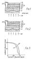
- the illustrated solar cell has a transparent substrate 11 of an insulator having first and second principal surfaces directed upwards and downwards of this figure, respectively.
- the transparent substrate 11 may be of soda-lime glass.
- a transparent conductive layer 12 is coated on the first principal surface of the substrate 11 and serves as an electrode of the solar cell.
- a combination of the substrate 11 and the transparent conductive layer 12 may be called a first member.
- the transparent conductive layer 12 may selectively be removed to form a pattern, if necessary.
- An amorphous silicon lamina 13 is attached to the transparent conductive layer 12 and comprises a P-type amorphous silicon layer 16 brought into contact with the transparent conductive layer 12, an N-type amorphous silicon layer 17 opposite to the P-type silicon layer 16, and an intrinsic silicon layer 18 interposed between the amorphous silicon layers 16 and 17.
- An aluminum layer 19 is deposited on the N-type silicon layer 17 and may be called a second member serving as another electrode of the solar cell.
- a pair of conductors 21 are derived from the first and the second members to be connected to a load (not shown).
- the second principal surface of the substrate 11 is directed towards light indicated by arrows 22.
- the light 22 is incident onto the amorphous silicon lamina 13 through the transparent substrate 11 and the transparent conductive layer 12.
- the amorphous silicon lamina 13 is activated by the incidence of light to develop electromotive force across the transparent conductive layer 12 and the aliminum layer 19.
- the electromotive force is derived from the conductors 21 as electric power.
- a solar cell according to a first embodiment of this invention comprises similar parts designated by like reference numerals.
- the illustrated solar cell comprises a specific transparent conductive layer 25 which comprises tin doped indium oxide, i.e. indium tin oxide.
- the illustrated indium tin oxide layer includes, by weight, 5% of tin oxide.
- the specific transparent conductive layer 25 is deposited to 700 angstroms thick by the use of vacuum evaporation and is formed by an aggregation of particles which have an average particle size not smaller than 300 angstroms.
- the vacuum evaporation is carried out with a pressure of oxygen and temperature of the substrate 11 kept at 10" Torr and 350°C, respectively.
- a deposit rate is about 1.5 angstroms/second.
- the particles are crystals of the indium tin oxide.
- the particles namely, the crystals are at first observed through a scanning electron microscope.
- a particle size of each particle is defined by a maximum size of each particle.
- a diameter, a transverse axis, and a diagonal are defined as the particle sizes when the particles are circular, elliptical, and rectangular, respectively.
- the particle sizes are calculated or accumulated to be divided by the number thereof only when the particle sizes are not smaller than 200 angstroms. In other words, such calculation takes no account of the other particles smaller than 200 angstroms.
- the illustrated conductive layer 25 has the average particle size of 300 angstroms.
- a sheet resistance of the specific transparent conductive layer 25 is about 30 ohms/ ⁇ .
- the specific transparent conductive layer 25 is undulated or uneven on the surface thereof, as diagrammatically illustrated in Fig. 2 in exaggeration and serves as the first member.
- an amorphous silicon lamina 13 is deposited. on the specific transparent conductive layer 25 by the use of a glow-discharge decomposition method known in the art.
- An aluminum layer 19 which serves as the second member is formed on the amorphous silicon lamina 13 by vacuum evaportion.
- the conductors 21 are connected to the first and the second members, respectively.
- a curve 30 shows a voltage versus current characteristic of the solar cell illustrated in conjunction with Fig. 2.
- a curve 31 shows a similar characteristic of a reference solar cell as illustrated in Fig. 1.
- the reference solar cell comprises the indium tin oxide layer having the average particle size smaller than 200 angstroms.
- the indium tin oxide layer in the conventional solar cell comprises the particles which are mostly smaller than 200 angstroms and which never exceed 300 angstroms.
- Each characteristic is measured by exposing each of the solar cells to light adjusted to AM1 (Air Mass 1).
- the fill factor and the conversion efficiency of the solar cell according to this invention are improved by about 20% and 20% as compared with those of the conventional solar cell, respectively.
- a contact area increases between the amorphous silicon lamina 13 and the specific or undulated transparent conductive layer 25 and, as a result, an improvement is possible of an electrical contact between them.
- the undulated conductive layer 25 serves to protect the light from being scattered from the amorphous silicon lamina 13. The light is therefore effectively utilized to excite the amorphous silicon lamina 13.
- the average particle size of 350 angstroms can be obtained under the pressure of 2 x 10 -4 Torr and the deposit rate of 1 angstrom/second while that of 800 angstroms, under the pressure of 10 4 Torr and the deposit rate of 0.5 angstrom/second.
- the number of the particles included in each sample may be equal to or more than 10/micron square and, preferably, is not less than 100/micron square. As mentioned before, each particle is not smaller than 200 angstroms.
- a particular factor d has been introduced so as to determine an upper limit of the average particle size.
- the specific transparent conductive layer 25 undulates with projections and notches formed on its surface.
- a thickness Ts is measured at each projection by the use of a usual thickness gauge of a probe type because a probe is larger than the projections and the notches.
- an average thickness Ta can be optically measured in a known manner.
- the above-mentioned particular factor ⁇ is defined by a difference between the thickness Ts of each projection and the average thickness Ta and may be called a difference factor.
- the difference factor has been between 100 and 650 angstroms, about 6% of the conversion efficiency has been accomplished and practically utilized as a solar cell.
- the difference factors A of 100 and 650 angstroms correspond to the average particle sizes of about 300 and 900 angstroms, respectively.
- the average particle size is preferably not larger than 900 angstroms.
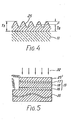
- a solar cell according to a second embodiment of this invention comprises, as the first electrode member, a conductive substrate 35 of a metal, such as stainless steel or the like.
- a specific transparent conductive layer 25' which is similar to that illustrated in conjunction with Fig. 2 is attached to the amorphous silicon lamina 13.
- the amorphous silicon lamina 13 is identical with that shown in Fig. 2.
- the specific transparent conductive layer 25' may be of indium tin oxide like in Fig. 2 and comprises an aggregation of particles which are not smaller in particle size than 300 angstroms.
- the transparent conductive layer 25' serves as the second member and is directed towards light 22, as shown in Fig. 5.
- a radio frequency (RF) reactive ion plating method may be carried out instead of the vacuum evaporation.
- RF radio frequency
- the average particle size tends to increase with a reduction of RF power.
- the average particle sizes become substantially equal to 300, 500, and 800 angstroms when the RF power was adjusted to 300, 200, and 100 watts, respectively, on condition that the substrate 11 or 35, the pressure of oxygen, and the deposit rate are kept at 300°C, 1 x 10 Torr, and 3 angstroms/second, respectively.
- a d.c. ion plating method, an activated reactive method, or the like may be employed to deposit the specific transparent conductive layer.
- the specific transparent conductive layer may singly comprise either indium oxide or tin oxide. Any other materials may be included in the specific transparent conductive layer.
- a plurality of the specific transparent conductive layers may be included in the solar cell.
Landscapes
- Photovoltaic Devices (AREA)
Abstract
Description
- This invention relates to a solar cell for use in converting optical energy into electric energy.
- A conventional solar cell of the type described comprises first and second members opposite to each other and an amorphous silicon lamina between the first and the second members. The first and the second members serve as electrodes. In such a solar cell, a predetermined one of the first and the second members should be transparent in order to expose the amorphous silicon lamina to light and to generate electromotive force across the first and the second members.
- It is preferable that the solar cell has a high conversion efficiency of optical energy to electric energy. Various kinds of attempts have been almost directed to improvement of characteristics of the amorphous silicon lamina so as to raise the conversion efficiency. In other words, such attemptq have almost left the first and the second members out of consideration. The conversion efficiency increases by improving characteristics of the amorphous silicon lamina to some extent. However, an increase of the conversion efficiency might reach a limit sooner or later in the above-mentioned manner. In addition, the conversion efficiency of each solar cell is seriously variable even when the amorphous silicon lamina is deposited on the same condition.
- It is an object of this invention to provide a solar cell which has an improved conversion efficiency.
- It is another object of this invention to provide a solar cell of the type described, which is capable of reducing a variation of the conversion efficiency.
- A solar cell to which this invention is applicable comprises a first and a second member and an amorphous silicon lamina between the first and the second members. A predetermined one of the first and the second members comprises a transparent conductive layer of a preselected material. According to this invention, the transparent conductive layer comprises an aggregation of particles of the preselected material which have an average particle size between 300 angstroms and 900 angstroms.
-
- Fig. 1 shows a sectional view of a conventional solar cell;
- Fig. 2 diagrammatically shows a sectional view of a solar cell according to a first embodiment of this invention;
- Fig. 3 shows voltage versus current characteristics of the conventional solar cell and the solar cell illustrated in Fig. 2;
- Fig. 4 shows a partial sectional view of the solar cell illustrated in Fig. 2; and
- Fig. 5 shows a sectional view of a solar cell according to a second embodiment of this invention.
- Referring to Fig. 1, a conventional solar cell will at first be described for a better understanding of this invention. The illustrated solar cell has a
transparent substrate 11 of an insulator having first and second principal surfaces directed upwards and downwards of this figure, respectively. Thetransparent substrate 11 may be of soda-lime glass. A transparentconductive layer 12 is coated on the first principal surface of thesubstrate 11 and serves as an electrode of the solar cell. A combination of thesubstrate 11 and the transparentconductive layer 12 may be called a first member. The transparentconductive layer 12 may selectively be removed to form a pattern, if necessary. - An
amorphous silicon lamina 13 is attached to the transparentconductive layer 12 and comprises a P-typeamorphous silicon layer 16 brought into contact with the transparentconductive layer 12, an N-typeamorphous silicon layer 17 opposite to the P-type silicon layer 16, and anintrinsic silicon layer 18 interposed between theamorphous silicon layers - An
aluminum layer 19 is deposited on the N-type silicon layer 17 and may be called a second member serving as another electrode of the solar cell. A pair ofconductors 21 are derived from the first and the second members to be connected to a load (not shown). - In the illustrated example, the second principal surface of the
substrate 11 is directed towards light indicated byarrows 22. As a result, thelight 22 is incident onto theamorphous silicon lamina 13 through thetransparent substrate 11 and the transparentconductive layer 12. Theamorphous silicon lamina 13 is activated by the incidence of light to develop electromotive force across the transparentconductive layer 12 and thealiminum layer 19. The electromotive force is derived from theconductors 21 as electric power. - In order to improve a conversion efficiency of the solar cell, various kinds of improvements have been contemplated about the
amorphous silicon lamina 13, as described in the preamble of the instant specification. - According to the inventor's experimental studies, it has been found out that the conversion efficiency is dependent not only on the
amorphous silicon lamina 13 but also on the transparentconductive layer 12, as will become clear. - Referring to Fig. 2, a solar cell according to a first embodiment of this invention comprises similar parts designated by like reference numerals. The illustrated solar cell comprises a specific transparent
conductive layer 25 which comprises tin doped indium oxide, i.e. indium tin oxide. The illustrated indium tin oxide layer includes, by weight, 5% of tin oxide. The specific transparentconductive layer 25 is deposited to 700 angstroms thick by the use of vacuum evaporation and is formed by an aggregation of particles which have an average particle size not smaller than 300 angstroms. The vacuum evaporation is carried out with a pressure of oxygen and temperature of thesubstrate 11 kept at 10" Torr and 350°C, respectively. A deposit rate is about 1.5 angstroms/second. The particles are crystals of the indium tin oxide. In order to determine the average particle size, the particles, namely, the crystals are at first observed through a scanning electron microscope. A particle size of each particle is defined by a maximum size of each particle. For example, a diameter, a transverse axis, and a diagonal are defined as the particle sizes when the particles are circular, elliptical, and rectangular, respectively. The particle sizes are calculated or accumulated to be divided by the number thereof only when the particle sizes are not smaller than 200 angstroms. In other words, such calculation takes no account of the other particles smaller than 200 angstroms. - As a result of the above-mentioned calculation, the illustrated
conductive layer 25 has the average particle size of 300 angstroms. A sheet resistance of the specific transparentconductive layer 25 is about 30 ohms/□. - The specific transparent
conductive layer 25 is undulated or uneven on the surface thereof, as diagrammatically illustrated in Fig. 2 in exaggeration and serves as the first member. - Like in Fig. 1, an
amorphous silicon lamina 13 is deposited. on the specific transparentconductive layer 25 by the use of a glow-discharge decomposition method known in the art. Analuminum layer 19 which serves as the second member is formed on theamorphous silicon lamina 13 by vacuum evaportion. Theconductors 21 are connected to the first and the second members, respectively. - Referring to Fig. 3, a
curve 30 shows a voltage versus current characteristic of the solar cell illustrated in conjunction with Fig. 2. On the other hand, acurve 31 shows a similar characteristic of a reference solar cell as illustrated in Fig. 1. The reference solar cell comprises the indium tin oxide layer having the average particle size smaller than 200 angstroms. Specifically, the indium tin oxide layer in the conventional solar cell comprises the particles which are mostly smaller than 200 angstroms and which never exceed 300 angstroms. - Each characteristic is measured by exposing each of the solar cells to light adjusted to AM1 (Air Mass 1).
- It is possible to estimate the characteristic of each solar cell by that absolute value of a reciprocal of a gradient at I = 0 which is represented by: |∂v/∂I|I=O, as known in the art. More particularly, the smaller the absolute value is, the better a solar cell is. Under the circumstances, it is readily understood that the solar cell according to the first embodiment of this invention is remarkably smaller in the absolute value than the conventional solar cell and, therefore, has an excellent characteristic in comparison with the conventional one. This means that the conversion efficiency is improved in the solar cell illustrated in Fig. 2 because a reduction of the absolute value contributes to a decrease of an internal resistance and, therefore, to an improvement of a fill factor.
- Practically, the fill factor and the conversion efficiency of the solar cell according to this invention are improved by about 20% and 20% as compared with those of the conventional solar cell, respectively. This is because a contact area increases between the
amorphous silicon lamina 13 and the specific or undulated transparentconductive layer 25 and, as a result, an improvement is possible of an electrical contact between them. In other words, the undulatedconductive layer 25 serves to protect the light from being scattered from theamorphous silicon lamina 13. The light is therefore effectively utilized to excite theamorphous silicon lamina 13. - In order to confirm or establish the relationship between the average particle size of the indium tin oxide and the voltage versus current characteristic, various samples were manufactured in the above-mentioned manner. When the samples had the average particle size of the indium tin oxide layer which was less than 300 angstroms, their voltage versus current characteristics were substantially identical to the
curve 31. When the average particle size exceeded 300 angstroms, the characteristics approached thecurve 30. From this fact, it has been contemplated that the average particle size of the indium tin oxide layer should not be smaller than 300 angstoms so as to improve the conversion factor in the solar cell. According to the inventor's experimental studies, the average particle size is possible by controlling the pressure of oxygen and the deposit rate with thesubstrate 11 kept at 350°C. For example, the average particle size of 350 angstroms can be obtained under the pressure of 2 x 10 -4 Torr and the deposit rate of 1 angstrom/second while that of 800 angstroms, under the pressure of 10 4 Torr and the deposit rate of 0.5 angstrom/second. - Consideration has been made about the number of the particles included in each sample. As a result, it has been found that the number of the particles may be equal to or more than 10/micron square and, preferably, is not less than 100/micron square. As mentioned before, each particle is not smaller than 200 angstroms.
- Referring to Fig. 4, a particular factor d has been introduced so as to determine an upper limit of the average particle size. As shown in Fig. 4, the specific transparent
conductive layer 25 undulates with projections and notches formed on its surface. A thickness Ts is measured at each projection by the use of a usual thickness gauge of a probe type because a probe is larger than the projections and the notches. On the other hand, an average thickness Ta can be optically measured in a known manner. The above-mentioned particular factor Δ is defined by a difference between the thickness Ts of each projection and the average thickness Ta and may be called a difference factor. When the difference factor has been between 100 and 650 angstroms, about 6% of the conversion efficiency has been accomplished and practically utilized as a solar cell. In addition, it has been found that the difference factors A of 100 and 650 angstroms correspond to the average particle sizes of about 300 and 900 angstroms, respectively. In this connection; the average particle size is preferably not larger than 900 angstroms. - Referring to Fig. 5, a solar cell according to a second embodiment of this invention comprises, as the first electrode member, a
conductive substrate 35 of a metal, such as stainless steel or the like. A specific transparent conductive layer 25' which is similar to that illustrated in conjunction with Fig. 2 is attached to theamorphous silicon lamina 13. Theamorphous silicon lamina 13 is identical with that shown in Fig. 2. The specific transparent conductive layer 25' may be of indium tin oxide like in Fig. 2 and comprises an aggregation of particles which are not smaller in particle size than 300 angstroms. In this solar cell, the transparent conductive layer 25' serves as the second member and is directed towardslight 22, as shown in Fig. 5. - With this structure also, the conversion efficiency has been improved when the average particle size is between 300 and 900 angstroms, as is the case with Fig. 2.
- Although the vacuum evaporation is used to deposit the specific transparent
conductive layer 25 or 25' in the first and the second embodiments, a radio frequency (RF) reactive ion plating method may be carried out instead of the vacuum evaporation. In this event, it has been found out that the average particle size tends to increase with a reduction of RF power. For example, the average particle sizes become substantially equal to 300, 500, and 800 angstroms when the RF power was adjusted to 300, 200, and 100 watts, respectively, on condition that thesubstrate - It is also possible to control the average particle size of the indium tin oxide by varying the pressure of oxygen and/or the deposit rate.
- While this invention has thus far been described in conjunction with a few embodiments thereof, it will readily be possible for those skilled in the art to put this invention into practice in various evaporation manners. For example, a d.c. ion plating method, an activated reactive method, or the like may be employed to deposit the specific transparent conductive layer. The specific transparent conductive layer may singly comprise either indium oxide or tin oxide. Any other materials may be included in the specific transparent conductive layer. A plurality of the specific transparent conductive layers may be included in the solar cell.
Claims (4)
(Claim 4 continued)
Applications Claiming Priority (2)
| Application Number | Priority Date | Filing Date | Title |
|---|---|---|---|
| JP213202/82 | 1982-12-04 | ||
| JP57213202A JPS59103384A (en) | 1982-12-04 | 1982-12-04 | Transparent conductive film for solar cells |
Publications (3)
| Publication Number | Publication Date |
|---|---|
| EP0112111A2 true EP0112111A2 (en) | 1984-06-27 |
| EP0112111A3 EP0112111A3 (en) | 1985-04-10 |
| EP0112111B1 EP0112111B1 (en) | 1991-03-06 |
Family
ID=16635221
Family Applications (1)
| Application Number | Title | Priority Date | Filing Date |
|---|---|---|---|
| EP83307383A Expired - Lifetime EP0112111B1 (en) | 1982-12-04 | 1983-12-05 | Solar cell |
Country Status (5)
| Country | Link |
|---|---|
| US (1) | US4568791A (en) |
| EP (1) | EP0112111B1 (en) |
| JP (1) | JPS59103384A (en) |
| AU (1) | AU561774B2 (en) |
| DE (1) | DE3382192D1 (en) |
Cited By (1)
| Publication number | Priority date | Publication date | Assignee | Title |
|---|---|---|---|---|
| DE4025311A1 (en) * | 1989-08-09 | 1991-02-14 | Sanyo Electric Co | PHOTOVOLTAIC INTERIOR |
Families Citing this family (11)
| Publication number | Priority date | Publication date | Assignee | Title |
|---|---|---|---|---|
| US4689438A (en) * | 1984-10-17 | 1987-08-25 | Sanyo Electric Co., Ltd. | Photovoltaic device |
| US4798808A (en) * | 1986-03-11 | 1989-01-17 | Atlantic Richfield Company | Photoconductive device coontaining electroless metal deposited conductive layer |
| JP2706113B2 (en) * | 1988-11-25 | 1998-01-28 | 工業技術院長 | Photoelectric conversion element |
| FR2680279A1 (en) * | 1991-08-09 | 1993-02-12 | Masse Georges | High-performance thermo-electronic device |
| US5986206A (en) * | 1997-12-10 | 1999-11-16 | Nanogram Corporation | Solar cell |
| JP2001060702A (en) * | 1999-06-18 | 2001-03-06 | Nippon Sheet Glass Co Ltd | Substrate for photoelectric conversion device and photoelectric conversion device using the same |
| US8586861B2 (en) * | 2003-01-12 | 2013-11-19 | 3Gsolar Photovoltaics Ltd. | Solar cell device |
| IL153895A (en) * | 2003-01-12 | 2013-01-31 | Orion Solar Systems Ltd | Solar cell device |
| US20060177567A1 (en) * | 2005-02-05 | 2006-08-10 | Winarski Tyson Y | Window that Generates Solar-powered Electricity via a Plurality of Noncontiguous Solar Cells |
| US9136404B2 (en) * | 2008-12-10 | 2015-09-15 | Iucf-Hyu (Industry-University Cooperation Foundation Hanyang University) | Solar cell capable of recycling a substrate and method for manufacturing the same |
| US20140150849A1 (en) * | 2012-11-30 | 2014-06-05 | Deutsche Cell Gmbh | Photovoltaic cell and method of production thereof |
Family Cites Families (4)
| Publication number | Priority date | Publication date | Assignee | Title |
|---|---|---|---|---|
| JPS5749278A (en) * | 1980-09-08 | 1982-03-23 | Mitsubishi Electric Corp | Amorphous silicone solar cell |
| CA1176740A (en) * | 1980-12-03 | 1984-10-23 | Yoshihisa Tawada | High-voltage photovoltaic cell having a hetero junction of amorphous semiconductor and amorphous silicon |
| JPS57126174A (en) * | 1981-01-27 | 1982-08-05 | Sumitomo Electric Ind Ltd | Thin film solar cell |
| JPS5857756A (en) * | 1981-10-01 | 1983-04-06 | Agency Of Ind Science & Technol | Amorphous silicon solar battery |
-
1982
- 1982-12-04 JP JP57213202A patent/JPS59103384A/en active Pending
-
1983
- 1983-12-05 EP EP83307383A patent/EP0112111B1/en not_active Expired - Lifetime
- 1983-12-05 AU AU21986/83A patent/AU561774B2/en not_active Ceased
- 1983-12-05 US US06/558,111 patent/US4568791A/en not_active Expired - Lifetime
- 1983-12-05 DE DE8383307383T patent/DE3382192D1/en not_active Expired - Fee Related
Cited By (1)
| Publication number | Priority date | Publication date | Assignee | Title |
|---|---|---|---|---|
| DE4025311A1 (en) * | 1989-08-09 | 1991-02-14 | Sanyo Electric Co | PHOTOVOLTAIC INTERIOR |
Also Published As
| Publication number | Publication date |
|---|---|
| AU561774B2 (en) | 1987-05-14 |
| JPS59103384A (en) | 1984-06-14 |
| US4568791A (en) | 1986-02-04 |
| EP0112111B1 (en) | 1991-03-06 |
| DE3382192D1 (en) | 1991-04-11 |
| EP0112111A3 (en) | 1985-04-10 |
| AU2198683A (en) | 1984-06-07 |
Similar Documents
| Publication | Publication Date | Title |
|---|---|---|
| EP0179556B1 (en) | Improved current collection structure for photovoltaic devices | |
| EP0684652B1 (en) | Photovoltaic element, electrode structure thereof, and process for producing the same | |
| AU694272B2 (en) | Photovoltaic element and method for producing the same | |
| US6008451A (en) | Photovoltaic device | |
| US7186479B2 (en) | Thin film battery and method of manufacture | |
| US5279682A (en) | Solar cell and method of making same | |
| US4623751A (en) | Photovoltaic device and its manufacturing method | |
| US4568791A (en) | Solar cell comprising an undulated transparent conductive layer | |
| US4338482A (en) | Photovoltaic cell | |
| EP4521468A1 (en) | Solar cell and preparation method therefor | |
| JP4222992B2 (en) | Photovoltaic device | |
| JP3287754B2 (en) | Method for forming metal electrode of solar cell | |
| EP0796498B1 (en) | Electrochemical photovoltaic cell | |
| US5064477A (en) | Radiant energy sensitive device and method | |
| JP3196155B2 (en) | Photovoltaic device | |
| EP0321136B1 (en) | Low light level solar cell | |
| JPS6245079A (en) | Substrate for solar cell and manufacture thereof | |
| CN120018600B (en) | Longitudinal photoconductive switch with electrode expansion structure and preparation method thereof | |
| JP2975751B2 (en) | Photovoltaic device | |
| JP2004158556A (en) | Solar cell | |
| JP3649948B2 (en) | Photovoltaic device and manufacturing method thereof | |
| JPH0548127A (en) | Amorphous silicon solar cell and manufacturing method thereof | |
| JPH06338223A (en) | Transparent conductive film | |
| CN112542530A (en) | Photovoltaic cell and preparation method thereof | |
| JP2815688B2 (en) | Manufacturing method of thin film solar cell |
Legal Events
| Date | Code | Title | Description |
|---|---|---|---|
| PUAI | Public reference made under article 153(3) epc to a published international application that has entered the european phase |
Free format text: ORIGINAL CODE: 0009012 |
|
| AK | Designated contracting states |
Designated state(s): DE FR GB IT |
|
| PUAL | Search report despatched |
Free format text: ORIGINAL CODE: 0009013 |
|
| AK | Designated contracting states |
Designated state(s): DE FR GB IT |
|
| 17P | Request for examination filed |
Effective date: 19851007 |
|
| 17Q | First examination report despatched |
Effective date: 19870722 |
|
| GRAA | (expected) grant |
Free format text: ORIGINAL CODE: 0009210 |
|
| AK | Designated contracting states |
Kind code of ref document: B1 Designated state(s): DE FR GB IT |
|
| ITF | It: translation for a ep patent filed | ||
| ET | Fr: translation filed | ||
| REF | Corresponds to: |
Ref document number: 3382192 Country of ref document: DE Date of ref document: 19910411 |
|
| PLBE | No opposition filed within time limit |
Free format text: ORIGINAL CODE: 0009261 |
|
| STAA | Information on the status of an ep patent application or granted ep patent |
Free format text: STATUS: NO OPPOSITION FILED WITHIN TIME LIMIT |
|
| 26N | No opposition filed | ||
| PGFP | Annual fee paid to national office [announced via postgrant information from national office to epo] |
Ref country code: GB Payment date: 19961204 Year of fee payment: 14 |
|
| PGFP | Annual fee paid to national office [announced via postgrant information from national office to epo] |
Ref country code: FR Payment date: 19961230 Year of fee payment: 14 |
|
| PGFP | Annual fee paid to national office [announced via postgrant information from national office to epo] |
Ref country code: DE Payment date: 19970227 Year of fee payment: 14 |
|
| PG25 | Lapsed in a contracting state [announced via postgrant information from national office to epo] |
Ref country code: GB Free format text: LAPSE BECAUSE OF NON-PAYMENT OF DUE FEES Effective date: 19971205 |
|
| PG25 | Lapsed in a contracting state [announced via postgrant information from national office to epo] |
Ref country code: FR Free format text: THE PATENT HAS BEEN ANNULLED BY A DECISION OF A NATIONAL AUTHORITY Effective date: 19971231 |
|
| GBPC | Gb: european patent ceased through non-payment of renewal fee |
Effective date: 19971205 |
|
| PG25 | Lapsed in a contracting state [announced via postgrant information from national office to epo] |
Ref country code: DE Free format text: LAPSE BECAUSE OF NON-PAYMENT OF DUE FEES Effective date: 19980901 |
|
| REG | Reference to a national code |
Ref country code: FR Ref legal event code: ST |