EP0111264A2 - Transmitting or receiving apparatus for opto-electrical communication equipment - Google Patents
Transmitting or receiving apparatus for opto-electrical communication equipment Download PDFInfo
- Publication number
- EP0111264A2 EP0111264A2 EP83112093A EP83112093A EP0111264A2 EP 0111264 A2 EP0111264 A2 EP 0111264A2 EP 83112093 A EP83112093 A EP 83112093A EP 83112093 A EP83112093 A EP 83112093A EP 0111264 A2 EP0111264 A2 EP 0111264A2
- Authority
- EP
- European Patent Office
- Prior art keywords
- tube
- glass fiber
- connecting piece
- transmitting
- receiving device
- Prior art date
- Legal status (The legal status is an assumption and is not a legal conclusion. Google has not performed a legal analysis and makes no representation as to the accuracy of the status listed.)
- Granted
Links
- 238000004891 communication Methods 0.000 title abstract description 3
- 239000003365 glass fiber Substances 0.000 claims abstract description 46
- 229910052751 metal Inorganic materials 0.000 claims abstract description 30
- 239000002184 metal Substances 0.000 claims abstract description 30
- 238000004519 manufacturing process Methods 0.000 claims description 10
- 238000005476 soldering Methods 0.000 claims description 10
- 239000013307 optical fiber Substances 0.000 claims description 8
- BASFCYQUMIYNBI-UHFFFAOYSA-N platinum Chemical compound [Pt] BASFCYQUMIYNBI-UHFFFAOYSA-N 0.000 claims description 7
- 238000001465 metallisation Methods 0.000 claims description 6
- VYZAMTAEIAYCRO-UHFFFAOYSA-N Chromium Chemical compound [Cr] VYZAMTAEIAYCRO-UHFFFAOYSA-N 0.000 claims description 4
- 230000005540 biological transmission Effects 0.000 claims description 4
- PCHJSUWPFVWCPO-UHFFFAOYSA-N gold Chemical compound [Au] PCHJSUWPFVWCPO-UHFFFAOYSA-N 0.000 claims description 4
- 229910052737 gold Inorganic materials 0.000 claims description 4
- 239000010931 gold Substances 0.000 claims description 4
- 229910052697 platinum Inorganic materials 0.000 claims description 3
- 239000000956 alloy Substances 0.000 claims 1
- 229910045601 alloy Inorganic materials 0.000 claims 1
- LQBJWKCYZGMFEV-UHFFFAOYSA-N lead tin Chemical compound [Sn].[Pb] LQBJWKCYZGMFEV-UHFFFAOYSA-N 0.000 claims 1
- 230000005693 optoelectronics Effects 0.000 abstract 1
- 230000003287 optical effect Effects 0.000 description 6
- 244000089486 Phragmites australis subsp australis Species 0.000 description 4
- 239000000835 fiber Substances 0.000 description 3
- 238000000034 method Methods 0.000 description 3
- 239000004065 semiconductor Substances 0.000 description 3
- 229910000679 solder Inorganic materials 0.000 description 3
- 125000006850 spacer group Chemical group 0.000 description 3
- 238000012546 transfer Methods 0.000 description 3
- 238000011161 development Methods 0.000 description 2
- 238000005538 encapsulation Methods 0.000 description 2
- 230000007704 transition Effects 0.000 description 2
- 229910000978 Pb alloy Inorganic materials 0.000 description 1
- 229910001128 Sn alloy Inorganic materials 0.000 description 1
- ATJFFYVFTNAWJD-UHFFFAOYSA-N Tin Chemical compound [Sn] ATJFFYVFTNAWJD-UHFFFAOYSA-N 0.000 description 1
- 238000004026 adhesive bonding Methods 0.000 description 1
- 238000005275 alloying Methods 0.000 description 1
- 230000008901 benefit Effects 0.000 description 1
- 230000007797 corrosion Effects 0.000 description 1
- 238000005260 corrosion Methods 0.000 description 1
- 238000013461 design Methods 0.000 description 1
- 238000005516 engineering process Methods 0.000 description 1
- 230000004907 flux Effects 0.000 description 1
- WABPQHHGFIMREM-UHFFFAOYSA-N lead(0) Chemical compound [Pb] WABPQHHGFIMREM-UHFFFAOYSA-N 0.000 description 1
- 238000012986 modification Methods 0.000 description 1
- 230000004048 modification Effects 0.000 description 1
- 230000035939 shock Effects 0.000 description 1
- 239000013589 supplement Substances 0.000 description 1
- 229910052718 tin Inorganic materials 0.000 description 1
- 229910001174 tin-lead alloy Inorganic materials 0.000 description 1
- 238000009736 wetting Methods 0.000 description 1
Images

Classifications
-
- G—PHYSICS
- G02—OPTICS
- G02B—OPTICAL ELEMENTS, SYSTEMS OR APPARATUS
- G02B6/00—Light guides; Structural details of arrangements comprising light guides and other optical elements, e.g. couplings
- G02B6/24—Coupling light guides
- G02B6/42—Coupling light guides with opto-electronic elements
- G02B6/4201—Packages, e.g. shape, construction, internal or external details
- G02B6/4219—Mechanical fixtures for holding or positioning the elements relative to each other in the couplings; Alignment methods for the elements, e.g. measuring or observing methods especially used therefor
- G02B6/4236—Fixing or mounting methods of the aligned elements
-
- G—PHYSICS
- G02—OPTICS
- G02B—OPTICAL ELEMENTS, SYSTEMS OR APPARATUS
- G02B6/00—Light guides; Structural details of arrangements comprising light guides and other optical elements, e.g. couplings
- G02B6/24—Coupling light guides
- G02B6/42—Coupling light guides with opto-electronic elements
- G02B6/4201—Packages, e.g. shape, construction, internal or external details
- G02B6/4202—Packages, e.g. shape, construction, internal or external details for coupling an active element with fibres without intermediate optical elements, e.g. fibres with plane ends, fibres with shaped ends, bundles
-
- G—PHYSICS
- G02—OPTICS
- G02B—OPTICAL ELEMENTS, SYSTEMS OR APPARATUS
- G02B6/00—Light guides; Structural details of arrangements comprising light guides and other optical elements, e.g. couplings
- G02B6/24—Coupling light guides
- G02B6/42—Coupling light guides with opto-electronic elements
- G02B6/4201—Packages, e.g. shape, construction, internal or external details
- G02B6/4248—Feed-through connections for the hermetical passage of fibres through a package wall
-
- G—PHYSICS
- G02—OPTICS
- G02B—OPTICAL ELEMENTS, SYSTEMS OR APPARATUS
- G02B6/00—Light guides; Structural details of arrangements comprising light guides and other optical elements, e.g. couplings
- G02B6/44—Mechanical structures for providing tensile strength and external protection for fibres, e.g. optical transmission cables
- G02B6/4401—Optical cables
- G02B6/4415—Cables for special applications
- G02B6/4427—Pressure resistant cables, e.g. undersea cables
- G02B6/4428—Penetrator systems in pressure-resistant devices
Definitions
- the invention relates to a transmitting and / or receiving device for devices of electro-optical communication, with an arrangement containing electrical switching means, which is housed in a metal housing and with a passage of an optical fiber designed as a glass fiber through an outer wall of the metal housing.
- Such a device is e.g. known from TELCOM Report 2 (1979), supplement “Digital transmission technology”, page 114.
- a pigtail bushing can be made by gluing.
- a hermetically sealed implementation cannot be easily achieved.
- a press seal is associated with relatively large mechanical loads on the fiber and is not sufficiently shock-resistant for various applications.
- the object of the invention is to design a transmitting and / or receiving device of the type mentioned at the outset such that there is a hermetically sealed passage of the glass fiber through the outer wall of the metal housing.
- the transmitting and / or receiving device for solving this problem is designed such that a metal tube is inserted into the outer wall of the metal housing for the hermetically sealed implementation of the glass fiber and that a metal, sleeve-shaped connecting piece is placed on the tube sides of the larger inner diameter with the outer surface of the tube and on the side of the smaller inner diameter with the through the connector and through the tube and at least in the region of the connector metallized glass fiber is hermetically sealed by means of a soldered connection.
- the metallization of the glass fiber preferably extends from the end face to a little beyond the connecting piece.
- the connecting piece is dimensioned such that it is easily displaceable on the tube before soldering.
- the connecting piece is placed on the tube outside the housing.
- a preferred method for producing a transmitting and / or receiving device with a connector arranged in this way is that the connector is first soldered to the glass fiber and that the prepared glass fiber is threaded into the tube and the connector is pushed over the tube and that the connector after adjustment and fixation of the glass fiber with the tube is soldered flux-free.
- a method for producing a transmitting and / or receiving device which can be used advantageously both with an arrangement of the connecting piece inside the housing and with an arrangement of the connecting piece outside the housing, consists in the fact that the connecting piece is produced the housing is placed on the tube and soldered and that the glass fiber is threaded into the tube and fixed after adjustment and that the glass fiber is soldered to the connector after fixing.
- the metallization of the glass fiber consists of several layers, with a chrome layer being followed by a platinum layer and this being followed by a gold layer and a layer of a tin-lead alloy.
- FIG. 1 shows the structure of a receiving device in which a PIN diode is arranged in a hermetically sealed circuit module and is optically coupled to an optical fiber.
- the receiving device shown in Fig. 1 is housed in the metal housing 11, which is closed with the lid 6.
- the spacer 12 lies on the bottom of the cuboid metal housing 11.
- the spacer 12 carries the circuit module 13, which is of plate-like shape and which is arranged parallel to the bottom of the metal housing 11 at the distance predetermined by the spacer 12.
- the tube 10 In a side wall of the metal housing 11, the tube 10 is attached, which projects outwards and inwards over the side wall of the metal housing 11.
- the sleeve-shaped connecting piece 9 On the outside, the sleeve-shaped connecting piece 9 is placed on the tube 10, which is placed on the tube with the larger opening and the optical waveguide 8 is guided in its smaller opening.
- the optical waveguide 8 runs through the connector 9, the tube 10 and through the block 5 an opening in the diode carrier 3 to the optical window of the PIN photodiode 2.
- the optical fiber 8 formed by a glass fiber is fixed at two points, namely on the block 5 and inside the connector 9 at the point where the sleeve-shaped connector has the smaller inside diameter Has.
- the diode carrier 3 is fastened to the circuit module 13 with two metal angles 1.
- the two metal angles 1, of which only one is visible in FIG. 1, are located next to the PIN diode 2.
- the PIN photodiode 2 which is used has an optical window with a diameter of about 30 to 200 / um in the center of the back-side and opposite to the front side of a bonding pad.
- the optical fiber receiving module 13 is housed in a hermetically sealed, metal housing 11.
- the metal housing 11 is provided with a hermetically sealed glass fiber bushing, so that there is a so-called pigtail connection for the optical transmission.
- the hermetic encapsulation which serves for shielding and / or for corrosion protection, is particularly expedient when using unprotected semiconductor components, in particular semiconductor chips.
- the glass fiber bushing consists of the tube 10 inserted into the outer wall of the housing 11 and the connecting piece 9 placed on the tube 10.
- the optical fiber 8 is threaded through the bushing and optically coupled to the PIN photodiode 2.
- the optical fiber 8 is precisely adjusted in front of the optical window and then fixed on the block 5.
- the glass fiber is soldered into the connector 9.
- the smaller hole diameter in the connector 9 is about 120 / um larger than the diameter of the glass fiber.
- a hole diameter of about 150 microns in the connector 9 is appropriate.
- the tube 10 advantageously has a much larger inside diameter, in particular approximately> 0.5 mm.
- the connecting piece 9 has the shape of a sleeve and, as a so-called solder sleeve, ensures a transition from a large to a small diameter. It consists of two hollow cylinders with a hollow conical part in between and is provided with a solderable surface on the inside. The sleeve has approximately the same wall thickness in all areas. One hollow cylinder fits on the pipe. The glass fiber fits into the other hollow cylinder, so that there is a transition from the inside diameter of the tube to the outside diameter of the glass fiber.
- the metallization has the advantage that no alloying occurs during soldering. At the same time, it offers effective mechanical protection of the glass fiber during handling.
- the connecting piece 9 on the tube 10 is easily displaceable in the axial direction of the glass fiber 8 or in the direction of the Z axis. After the glass fiber 8 is adjusted and fixed, the connector 9 is soldered to the tube 10 without flux.
- the receiving device shown in the figures contains a PIN photodiode as the receiving diode.
- the receiving diode is used as the transmitting diode, for example a laser diode or light-emitting diode.
Landscapes
- Physics & Mathematics (AREA)
- General Physics & Mathematics (AREA)
- Optics & Photonics (AREA)
- Optical Couplings Of Light Guides (AREA)
- Telephone Function (AREA)
- Measuring Pulse, Heart Rate, Blood Pressure Or Blood Flow (AREA)
- Electrotherapy Devices (AREA)
- Light Guides In General And Applications Therefor (AREA)
- Mounting And Adjusting Of Optical Elements (AREA)
Abstract
Description
Die Erfindung bezieht sich auf eine Sende- und/oder Empfangsvorrichtung für Einrichtungen der elektrooptischen Nachrichtenübertragung, mit einer elektrische Schaltmittel enthaltenden Anordnung, die in einem Metallgehäuse untergebracht ist und mit einer Durchführung eines als Glasfaser ausgebildeten Lichtwellenleiters durch eine Außenwand des Metallgehäuses.The invention relates to a transmitting and / or receiving device for devices of electro-optical communication, with an arrangement containing electrical switching means, which is housed in a metal housing and with a passage of an optical fiber designed as a glass fiber through an outer wall of the metal housing.
Eine derartige Vorrichtung ist z.B. aus TELCOM-Report 2 (1979), Beiheft "Digital-Übertragungstechnik", Seite 114 bekannt.Such a device is e.g. known from TELCOM Report 2 (1979), supplement "Digital transmission technology", page 114.
Bei derartigen Sende- und/oder Empfangsvorrichtungen kann es, insbesondere im Hinblick auf eine Verwendung ungeschützter Halbleiterbauelemente erforderlich werden, ein Schaltungsmodul mit optisch gekoppeltem, durch eine Glasfaser gebildeten Lichtwellenleiter in einem hermetisch dichten Metallgehäuse unterzubringen. In diesem Fall ist eine hermetisch dichte Durchführung der Glasfaser durch eine Außenwand des Metallgehäuses erforderlich.In the case of such transmission and / or reception devices, in particular with regard to the use of unprotected semiconductor components, it may be necessary to accommodate a circuit module with an optically coupled optical fiber formed by a glass fiber in a hermetically sealed metal housing. In this case, a hermetically sealed passage of the glass fiber through an outer wall of the metal housing is required.
Man kann eine Pigtail-Durchführung durch Kleben herstellen. Dabei läßt sich jedoch eine hermetisch dichte Durchführung nicht ohne weiteres erzielen. Eine Preßdichtung ist mit relativ großen mechanischen Belastungen der Faser verbunden und für verschiedene Anwendungsfälle nicht ausreichend schockbeständig. Schließlich haben Untersuchungen im Rahmen der Erfindung ergeben, daß sich beim Löten mit einem Löttropfen eine schlechte Benetzung der Glasfaser durch schlechten Wärmeübergang an der Faser ergeben kann.A pigtail bushing can be made by gluing. However, a hermetically sealed implementation cannot be easily achieved. A press seal is associated with relatively large mechanical loads on the fiber and is not sufficiently shock-resistant for various applications. Finally, studies within the scope of the invention have shown that poor soldering of the glass fiber occurs when soldering with a drop of solder due to poor heat transfer to the fiber.
Aufgabe der Erfindung ist es, eine Sende- und/oder Empfangsvorrichtung der eingangs genannten Art derart auszubilden, daß sich eine hermetisch dichte Durchführung der Glasfaser durch die Außenwand des Metallgehäuses ergibt.The object of the invention is to design a transmitting and / or receiving device of the type mentioned at the outset such that there is a hermetically sealed passage of the glass fiber through the outer wall of the metal housing.
Gemäß der Erfindung wird die Sende- und/oder Empfangsvorrichtung zur Lösung dieser Aufgabe derart ausgebildet, daß in die Außenwand des Metallgehäuses zur hermetisch dichten Durchführung der Glasfaser ein metallenes Rohr eingesetzt ist und daß auf das Rohr ein metallenes, muffenförmiges Verbindungsstück aufgesetzt ist, das auf seiten des größeren Innendurchmessers mit der Außenfläche des Rohres und auf seiten des kleineren Innendurchmessers mit der durch das Verbindungsstück und durch das Rohr hindurchgeführten und wenigstens im Bereich des Verbindungsstückes metallisierten Glasfaser mittels einer Lötverbindung hermetisch dicht verbunden ist. Die Metallisierung der Glasfaser erstreckt sich vorzugsweise von der Stirnseite bis etwas über das Verbindungsstück hinaus.According to the invention, the transmitting and / or receiving device for solving this problem is designed such that a metal tube is inserted into the outer wall of the metal housing for the hermetically sealed implementation of the glass fiber and that a metal, sleeve-shaped connecting piece is placed on the tube sides of the larger inner diameter with the outer surface of the tube and on the side of the smaller inner diameter with the through the connector and through the tube and at least in the region of the connector metallized glass fiber is hermetically sealed by means of a soldered connection. The metallization of the glass fiber preferably extends from the end face to a little beyond the connecting piece.
Durch diese Maßnahmen ergibt sich eine besonders hochwertige hermetisch dichte Durchführung der Glasfaser durch die Metallwand. Von besonderem Vorteil ist die gute Benetzung der Faser im kleinen Lötspalt und der besonders gute Wärmeübergang vom Verbindungsstück zur Glasfaser. Darüber hinaus ist die kurze Ausnehmung in dem Verbindungsstück erheblich leichter zu vergolden als das unvermeidlich längere Durchführungsrohr im Gehäuse.These measures result in a particularly high-quality hermetically sealed passage of the glass fiber through the metal wall. The good wetting of the fiber in the small soldering gap and the particularly good heat transfer from the connector to the glass fiber are particularly advantageous. In addition, the short recess in the connecting piece is considerably easier to gold-plate than the inevitably longer lead-through tube in the housing.
In weiterer Ausgestaltung der Erfindung wird das Verbindungsstück derart bemessen, daß es vor dem Verlöten auf dem Rohr leicht verschiebbar ist. Bei einer derartigen Ausgestaltung der Sende- und/oder Empfangsvorrichtung läßt sich das Ende der Glasfaser vor dem zugeordneten Sende- und /oder Empfangselement durch einfaches Verschieben des Verbindungsstückes auf einfache Weise fein justieren.In a further embodiment of the invention, the connecting piece is dimensioned such that it is easily displaceable on the tube before soldering. With such a configuration of the transmitting and / or receiving device the end of the glass fiber in front of the assigned transmitting and / or receiving element can be finely adjusted in a simple manner by simply moving the connecting piece.
In Weiterbildung der Erfindung ist das Verbindungsstück außerhalb des Gehäuses auf das Rohr aufgesetzt. Ein bevorzugtes Verfahren zur Herstellung einer Sende- und/oder Empfangsvorrichtung mit einem derart angeordneten Verbindungsstück besteht darin, daß das Verbindungsstück zuerst an der Glasfaser angelötet wird und daß die vorbereitete Glasfaser in das Rohr eingefädelt und das Verbindungsstück über das Rohr geschoben wird und daß das Verbindungsstück nach Justierung und Fixierung der Glasfaser mit dem Rohr flußmittelfrei verlötet wird.In a further development of the invention, the connecting piece is placed on the tube outside the housing. A preferred method for producing a transmitting and / or receiving device with a connector arranged in this way is that the connector is first soldered to the glass fiber and that the prepared glass fiber is threaded into the tube and the connector is pushed over the tube and that the connector after adjustment and fixation of the glass fiber with the tube is soldered flux-free.
Andererseits kann es sich als zweckmäßig erweisen, das Verbindungsstück im Inneren des Gehäuses auf das Rohr aufzusetzen.On the other hand, it may prove expedient to place the connector on the inside of the housing.
Ein Verfahren zur Herstellung einer Sende- und/oder Empfangsvorrichtung, das sowohl bei einer Anordnung des Verbindungsstückes innerhalb des Gehäuses als auch bei einer Anordnung des Verbindungsstückes außerhalb des Gehäuses vorteilhaft verwendbar ist, besteht in weiterer Ausgestaltung der Erfindung darin, daß das Verbindungsstück bei der Herstellung des Gehäuses auf das Rohr aufgesetzt und angelötet wird und daß die Glasfaser in das Rohr eingefädelt und nach Justierung fixiert wird und daß die Glasfaser nach der Fixierung an dem Verbindungsstück verlötet wird.In a further embodiment of the invention, a method for producing a transmitting and / or receiving device, which can be used advantageously both with an arrangement of the connecting piece inside the housing and with an arrangement of the connecting piece outside the housing, consists in the fact that the connecting piece is produced the housing is placed on the tube and soldered and that the glass fiber is threaded into the tube and fixed after adjustment and that the glass fiber is soldered to the connector after fixing.
In Weiterbildung der Erfindung besteht die Metallisierung der Glasfaser aus mehreren Schichten, wobei auf eine Chromschicht eine Platinschicht und auf diese eine Goldschicht und eine Schicht aus einer Zinn-Blei-Legierung folgen.In a further development of the invention, the metallization of the glass fiber consists of several layers, with a chrome layer being followed by a platinum layer and this being followed by a gold layer and a layer of a tin-lead alloy.
Die Erfindung wird anhand der in den Figuren dargestellten Ausführungsbeispiele näher- erläutert.The invention is explained in greater detail on the basis of the exemplary embodiments illustrated in the figures.
Fig. 1 zeigt den Aufbau einer Empfangsvorrichtung, bei der eine PIN-Diode in einem hermetisch dicht gekapselten Schaltungsmodul angeordnet und mit einer Glasfaser optisch gekoppelt ist.1 shows the structure of a receiving device in which a PIN diode is arranged in a hermetically sealed circuit module and is optically coupled to an optical fiber.
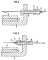
Einzelheiten der Empfangsvorrichtung nach Fig. 1 gehen aus den Figuren 2 und 3 hervor. Dabei zeigen
- Fig. 2 weitere Einzelheiten der Durchführung der Glasfaser durch die Außenwand eines hermetisch dichten Metallgehäuses und
- Fig. 3 eine Abwandlung der in Fig. 1 gezeigten Empfangsvorrichtung in der Weise, daß das Verbindungsstück im Innern anstatt außerhalb des metallischen Gehäuses angeordnet ist.
- Fig. 2 further details of the implementation of the glass fiber through the outer wall of a hermetically sealed metal housing and
- Fig. 3 shows a modification of the receiving device shown in Fig. 1 in such a way that the connecting piece is arranged inside instead of outside the metallic housing.
Die in Fig. 1 gezeigte Empfangsvorrichtung ist in dem Metallgehäuse 11 untergebracht, das mit dem Deckel 6 verschlossen ist. Auf dem Boden des quaderförmigen Metallgehäuses 11 liegt das Abstandsstück 12. Das Abstandsstück 12 trägt den Schaltungsmodul 13, der von plattenförmiger Gestalt ist und der in dem durch das Abstandsstück 12 vorgegebenen Abstand parallel zum Boden des Metallgehäuses 11 angeordnet ist.The receiving device shown in Fig. 1 is housed in the
In einer Seitenwand des Metallgehäuses 11 ist das Rohr 10 angebracht, das nach außen und nach innen über die Seitenwand des Metallgehäuses 11 hinausragt. Außen ist auf das Rohr 10 das muffenförmige Verbindungsstück 9 aufgesetzt, das mit der größeren Öffnung auf das Rohr aufgesetzt ist und in dessen kleinerer Öffnung der Lichtwellenleiter 8 geführt ist. Der Lichtwellenleiter 8 verläuft durch das Verbindungsstück 9, das Rohr 10 und über den Klotz 5 durch eine öffnung im Diodenträger 3 zum optischen Fenster der PIN-Fotodiode 2. Der durch eine Glasfaser gebildete Lichtwellenleiter 8 ist dabei an zwei Stellen fixiert, nämlich auf dem Klotz 5 und im Innern des Verbindungsstückes 9 an der Stelle, wo das muffenförmige Verbindungsstück den kleineren Innendurchmesser hat.In a side wall of the
Der Diodenträger 3 ist mit zwei Metallwinkeln 1 auf dem Schaltungsmodul 13 befestigt. Die beiden Metallwinkel 1, von denen in Fig. 1 nur einer sichtbar ist, befinden sich dabei neben der PIN-Diode 2.The diode carrier 3 is fastened to the
Die verwendete PIN-Fotodiode 2 hat ein optisches Fenster mit einem Durchmesser von etwa 30 bis 200 /um in der Mitte der Rückseitenkontaktierung und gegenüber auf der Vorderseite ein Bondpad.The PIN photodiode 2 which is used has an optical window with a diameter of about 30 to 200 / um in the center of the back-side and opposite to the front side of a bonding pad.
Der Lichtwellenleiter-Empfangsmodul 13 ist in einem hermetisch dichten, metallenen Gehäuse 11 untergebracht. Das Metallgehäuse 11 ist mit einer hermetisch dichten Glasfaserdurchführung versehen, so daß sich ein sogenannter Pigtail-Anschluß für die optische Übertragung ergibt. Die hermetische Kapselung, die zur Schirmung und/oder zum Korrosionsschutz dient, ist insbesondere bei einem Einsatz von ungeschützten Halbleiterbauelementen, insbesondere Halbleiterchips zweckmäßig.The optical
Die Glasfaserdurchführung besteht aus dem in die Außenwand des Gehäuses 11 eingesetzten Rohr 10 und dem auf das Rohr 10 aufgesetzten Verbindungsstück 9.The glass fiber bushing consists of the
Nach dem Einbau des Schaltungsmoduls 13 in das Gehäuse 11 wird die Glasfaser 8 durch die Durchführung gefädelt und an die PIN-Fotodiode 2 optisch gekoppelt. Der Lichtwellenleiter 8 wird dabei vor dem optischen Fenster exakt justiert und anschließend auf dem Klotz 5 fixiert.After the
Um eine hermetische Dichtung zu erreichen, wird die Glasfaser in das Verbindungsstück 9 eingelötet. Der kleinere Lochdurchmesser im Verbindungsstück 9 ist etwa 120 /um größer als der Durchmesser der Glasfaser. Für eine Glasfaser mit einem Außendurchmesser von 125 µm ist ein Lochdurchmesser von etwa 150 µm im Verbindungsstück 9 zweckmäßig. Das Rohr 10 hat in vorteilhafter Weise einen wesentlich größeren Innendurchmesser, insbesondere etwa > 0,5 mm.In order to achieve a hermetic seal, the glass fiber is soldered into the
Das Verbindungsstück 9 hat die Form einer Muffe und sorgt als sogenannte Lötmuffe für einen übergang von einem großen auf einen kleinen Durchmesser. Es besteht aus zwei Hohlzylindern mit einem dazwischenliegenden hohlkegelförmigen Teil und ist innen mit einer lötbaren Oberfläche versehen. Die Muffe hat in allen Bereichen etwa die gleiche Wandstärke. Der eine Hohlzylinder paßt auf das Rohr. In den anderen Hohlzylinder paßt die Glasfaser, so daß sich ein Übergang vom Innendurchmesser des Rohres auf den Außendurchmesser der Glasfaser ergibt.The connecting
Dadurch ergibt sich ein sehr kleiner Lötspalt mit einem besonders guten Wärmeübergang von der Lötmuffe zur Glasfaser 8. Aus diesem Grunde, ist die hermetische Kapselung des -Gehäuses 11 mit Hilfe des Verbindungsstückes 9 erheblich erleichtert.This results in a very small soldering gap with a particularly good heat transfer from the soldering sleeve to the
Bei der in Fig. 2 gezeigten Vorrichtung befindet sich das Verbindungsstück 9 außerhalb des Gehäuses 11. Diese Vorrichtung wird vorzugsweise auf die folgende Art hergestellt:
- Zunächst wird die Lötmuffe bzw. das
Verbindungsstück 9 an derGlasfaser 8 angelötet. Dann wird dievorbereitete Glasfaser 9 insbesondere mit einer Metallisierung mit aufeinanoerfolgenden Schichten aus Chrom, Platin und Gold bedampft und mit einer Legierung aus Zinn und Blei tauchverzinnt, wobei die Schichtdicken vorzugsweise 30, 100 und 1000 und 1000 nm betragen. Nach dem Metallisieren wird dieGlasfaser 8 stirnseitig gebrochen und mit demangelöteten Verbindungsstück 9 in dasRohr 10 eingefädelt. Daraufhin wird dasVerbindungsstück 9 über dasRohr 10 geschoben und mit diesem durch Löten verbunden.
- First, the solder sleeve or the
connector 9 is soldered to theglass fiber 8. Then the preparedglass fiber 9 is vapor-deposited in particular with a metallization with successive layers of chrome, platinum and gold and with an alloy of tin and lead dip-tinned, the layer thicknesses preferably being 30, 100 and 1000 and 1000 nm. After the metallization, theglass fiber 8 is broken on the end face and threaded into thetube 10 with the soldered connectingpiece 9. Then theconnector 9 is pushed over thetube 10 and connected to it by soldering.
Die Metallisierung hat den Vorteil, daß beim Löten kein Ablegieren auftritt. Zugleich bietet sie einen wirksamen mechanischen Schutz der Glasfaser bei der Handhabung.The metallization has the advantage that no alloying occurs during soldering. At the same time, it offers effective mechanical protection of the glass fiber during handling.
Bei der Feinjustierung des Endes der Glasfaser 8 vor der PIN-Diode 2 ist das Verbindungsstück 9 am Rohr 10 in achsialer Richtung der Glasfaser 8 bzw. in Richtung der Z-Achse leicht verschiebbar. Nachdem die Glasfaser 8 justiert und fixiert ist, wird das Verbindungsstück 9 mit dem Rohr 10 flußmittelfrei verlötet.During the fine adjustment of the end of the
Bei der in Fig. 3 gezeigten Vorrichtung ist das Verbindungsstück 9 im Innern des Gehäuses 11 untergebracht. Diese Vorrichtung wird vorzugsweise nach dem folgenden Verfahren hergestellt:
Das Verbindungsstück 9 wird bereits bei der Herstellung des Gehäuses "11 auf das Rohr.10 innen auf der Innenseite des Gehäuses 11 angelötet. Anschließend wird das ganze Gehäuse 11 vergoldet.Die Glasfaser 8 wird in die Durchführung, bestehend ausdem Rohr 10und dem Verbindungsstück 9 eingefädelt, an der PIN-Fotodiode 2 justiert, fixiert und anschließend andem Verbindungsstück 9 verlötet.
- The
connector 9 is already soldered to thetube 10 inside on the inside of thehousing 11 during the manufacture of thehousing 11. Theentire housing 11 is then gold-plated 9 threaded, adjusted on the PIN photodiode 2, fixed and then soldered to theconnector 9.
Das in Verbindung mit der Herstellung der Vorrichtung nach Fig. 3 beschriebene Verfahren läßt sich vorteilhaft auch zur Herstellung der in Fig. 2 gezeigten Vorrichtung anwenden. Abgesehen davon, daß in diesem Fall das Verbindungsstück 9 zunächst anstatt im Innern außerhalb des Gehäuses 11 angelötet wird, laufen die weiteren Verfahrensschritte dabei wie beschrieben ab.The method described in connection with the manufacture of the device according to FIG. 3 can advantageously also be used for the manufacture of the device shown in FIG. 2. Apart from the fact that in this case the connecting
Die in den Figuren dargestellte Empfangsvorrichtung enthält eine PIN-Fotodiode als Empfangsdiode. Bei einer Sendevorrichtung tritt an die Stelle der Empfangsdiode als Sendediode beispielsweise eine Laserdiode oder lichtemittierende Diode.The receiving device shown in the figures contains a PIN photodiode as the receiving diode. In the case of a transmitting device, the receiving diode is used as the transmitting diode, for example a laser diode or light-emitting diode.
Claims (8)
Priority Applications (1)
| Application Number | Priority Date | Filing Date | Title |
|---|---|---|---|
| AT83112093T ATE21775T1 (en) | 1982-12-03 | 1983-12-01 | TRANSMITTER AND/OR RECEIVER DEVICE FOR ELECTRO-OPTICAL COMMUNICATION TRANSMISSION EQUIPMENT. |
Applications Claiming Priority (2)
| Application Number | Priority Date | Filing Date | Title |
|---|---|---|---|
| DE3244867 | 1982-12-03 | ||
| DE19823244867 DE3244867A1 (en) | 1982-12-03 | 1982-12-03 | TRANSMITTER AND / OR RECEIVING DEVICE FOR ELECTROOPTIC MESSAGE TRANSMISSION DEVICES |
Publications (3)
| Publication Number | Publication Date |
|---|---|
| EP0111264A2 true EP0111264A2 (en) | 1984-06-20 |
| EP0111264A3 EP0111264A3 (en) | 1984-08-08 |
| EP0111264B1 EP0111264B1 (en) | 1986-08-27 |
Family
ID=6179780
Family Applications (1)
| Application Number | Title | Priority Date | Filing Date |
|---|---|---|---|
| EP83112093A Expired EP0111264B1 (en) | 1982-12-03 | 1983-12-01 | Transmitting or receiving apparatus for opto-electrical communication equipment |
Country Status (5)
| Country | Link |
|---|---|
| US (1) | US4591711A (en) |
| EP (1) | EP0111264B1 (en) |
| JP (1) | JPS59113408A (en) |
| AT (1) | ATE21775T1 (en) |
| DE (2) | DE3244867A1 (en) |
Cited By (8)
| Publication number | Priority date | Publication date | Assignee | Title |
|---|---|---|---|---|
| EP0137485A2 (en) * | 1983-10-12 | 1985-04-17 | Siemens Aktiengesellschaft | Glas fibre feed-through for an opening in a box |
| EP0213426A1 (en) * | 1985-08-30 | 1987-03-11 | Siemens Aktiengesellschaft | Casing with a lower and an upper cap for an electrical circuit element |
| EP0214464A1 (en) * | 1985-09-05 | 1987-03-18 | Siemens Aktiengesellschaft | Casing for an optoelectronic circuit module |
| EP0216174A1 (en) * | 1985-09-25 | 1987-04-01 | Siemens Aktiengesellschaft | Light-directive coupling unit |
| DE3606588A1 (en) * | 1986-02-28 | 1987-09-03 | Siemens Ag | Gas-tight feedthrough of a glass fibre |
| EP0267536A2 (en) * | 1986-11-12 | 1988-05-18 | Alcatel SEL Aktiengesellschaft | Hermetically sealed connecting passage for glass fibre |
| EP0511931A2 (en) * | 1991-04-29 | 1992-11-04 | International Business Machines Corporation | An apparatus and a method for an optical fiber interface |
| US5241614A (en) * | 1991-04-29 | 1993-08-31 | International Business Machines Corporation | Apparatus and a method for an optical fiber interface |
Families Citing this family (24)
| Publication number | Priority date | Publication date | Assignee | Title |
|---|---|---|---|---|
| DE3244882A1 (en) * | 1982-12-03 | 1984-06-07 | Siemens AG, 1000 Berlin und 8000 München | TRANSMITTER OR RECEIVER WITH A DIODE HOLDED BY MEANS OF A CARRIER |
| EP0148012B1 (en) * | 1983-12-26 | 1988-11-02 | Kabushiki Kaisha Toshiba | Optical-fiber coupling device |
| JPS6123379A (en) * | 1984-07-11 | 1986-01-31 | Hitachi Ltd | Optoelectronic apparatus |
| US4726507A (en) * | 1984-08-29 | 1988-02-23 | The United States Of America As Represented By The Secretary Of The Air Force | Cryogenic glass-to-metal seal |
| DE3445982A1 (en) * | 1984-12-17 | 1986-06-19 | Siemens AG, 1000 Berlin und 8000 München | Glass fibre for an optical telecommunications line |
| US4722586A (en) * | 1985-04-12 | 1988-02-02 | Tektronix, Inc. | Electro-optical transducer module |
| US4814603A (en) * | 1985-06-24 | 1989-03-21 | Philips Gerald J | Method and apparatus for determining the size of defects in rolling element bearings with high frequency capability |
| DE3525480A1 (en) * | 1985-07-17 | 1987-01-29 | Kabelmetal Electro Gmbh | Process for coating a glass fibre with metal |
| US4802178A (en) * | 1986-04-10 | 1989-01-31 | Ortel Corporation | High speed fiberoptic laser module |
| US4803361A (en) * | 1986-05-26 | 1989-02-07 | Hitachi, Ltd. | Photoelectric device with optical fiber and laser emitting chip |
| DE3628391A1 (en) * | 1986-08-21 | 1988-02-25 | Licentia Gmbh | Gas-tight housing feedthrough (bushing) for a silica-glass optical fibre, and method for producing it |
| US5177806A (en) * | 1986-12-05 | 1993-01-05 | E. I. Du Pont De Nemours And Company | Optical fiber feedthrough |
| US4870271A (en) * | 1987-02-06 | 1989-09-26 | Philips Gerald J | Method and apparatus for determining the size of defects in rolling element bearings with high frequency capability |
| US4782226A (en) * | 1987-07-06 | 1988-11-01 | Semi-Gas Systems, Inc. | Optoelectronic chemical reaction detector |
| US4826276A (en) * | 1987-07-17 | 1989-05-02 | E. I. Du Pont De Nemours And Company | Optical fiber feedthrough assembly having a rigidizing arrangement therein |
| US4865410A (en) * | 1988-01-25 | 1989-09-12 | E. I. Du Pont De Nemours And Company | Decoupled fiber optic feedthrough assembly |
| US5011256A (en) * | 1988-10-28 | 1991-04-30 | E. I. Du Pont De Nemours And Company | Package for an opto-electronic component |
| US4979787A (en) * | 1990-01-12 | 1990-12-25 | Pco, Inc. | Optical-electronic interface module |
| JPH10319278A (en) * | 1997-05-16 | 1998-12-04 | Nec Corp | Optical coupling circuit |
| US6325551B1 (en) | 1999-12-08 | 2001-12-04 | New Focus, Inc. | Method and apparatus for optically aligning optical fibers with optical devices |
| US6632029B1 (en) | 1999-12-22 | 2003-10-14 | New Focus, Inc. | Method & apparatus for packaging high frequency components |
| US6786652B2 (en) * | 2001-12-19 | 2004-09-07 | Northrop Grumman Corporation | Process for fabricating a photonics package and for aligning an optical fiber with a photodetector surface during fabrication of such a package |
| JP5034353B2 (en) * | 2006-07-26 | 2012-09-26 | 富士通オプティカルコンポーネンツ株式会社 | Optical device manufacturing method |
| CN101697025B (en) * | 2009-10-26 | 2012-05-30 | 西北核技术研究所 | Direct-pass type optical fiber sealing device and method for manufacturing same |
Citations (4)
| Publication number | Priority date | Publication date | Assignee | Title |
|---|---|---|---|---|
| US4119363A (en) * | 1976-03-18 | 1978-10-10 | Bell Telephone Laboratories Incorporated | Package for optical devices including optical fiber-to-metal hermetic seal |
| GB2034068A (en) * | 1978-10-06 | 1980-05-29 | Kokusai Denshin Denwa Co Ltd | Feeding optical submarine cable into repeater |
| CA1108900A (en) * | 1978-09-15 | 1981-09-15 | Paul P. Webb | Electro-optic device housing for fiber-optic applications |
| DE3010820A1 (en) * | 1980-03-20 | 1981-09-24 | Siemens AG, 1000 Berlin und 8000 München | Support clamp for optical conductor end - uses capillary with planar outer surface adhered to clamp for e.g. laser diode coupling |
Family Cites Families (6)
| Publication number | Priority date | Publication date | Assignee | Title |
|---|---|---|---|---|
| JPS50153650A (en) * | 1974-05-30 | 1975-12-10 | ||
| US4118100A (en) * | 1975-12-10 | 1978-10-03 | International Telephone And Telegraph Corporation | Optical couplers for light emitting diodes and detectors |
| US4222629A (en) * | 1978-03-27 | 1980-09-16 | Sperry Corporation | Fiber optic connector assembly |
| US4346294A (en) * | 1979-07-05 | 1982-08-24 | Burr-Brown Research Corp. | Low profile optical coupling to planar-mounted optoelectronic device |
| NL7908536A (en) * | 1979-11-23 | 1981-06-16 | Philips Nv | COVER FOR A PICTURE DIOD. |
| NL8102050A (en) * | 1981-04-27 | 1982-11-16 | Philips Nv | FIBERGLASS TRANSIT IN A METAL HOUSING. |
-
1982
- 1982-12-03 DE DE19823244867 patent/DE3244867A1/en not_active Withdrawn
-
1983
- 1983-11-14 US US06/551,460 patent/US4591711A/en not_active Expired - Fee Related
- 1983-12-01 EP EP83112093A patent/EP0111264B1/en not_active Expired
- 1983-12-01 AT AT83112093T patent/ATE21775T1/en active
- 1983-12-01 DE DE8383112093T patent/DE3365724D1/en not_active Expired
- 1983-12-02 JP JP58227107A patent/JPS59113408A/en active Pending
Patent Citations (4)
| Publication number | Priority date | Publication date | Assignee | Title |
|---|---|---|---|---|
| US4119363A (en) * | 1976-03-18 | 1978-10-10 | Bell Telephone Laboratories Incorporated | Package for optical devices including optical fiber-to-metal hermetic seal |
| CA1108900A (en) * | 1978-09-15 | 1981-09-15 | Paul P. Webb | Electro-optic device housing for fiber-optic applications |
| GB2034068A (en) * | 1978-10-06 | 1980-05-29 | Kokusai Denshin Denwa Co Ltd | Feeding optical submarine cable into repeater |
| DE3010820A1 (en) * | 1980-03-20 | 1981-09-24 | Siemens AG, 1000 Berlin und 8000 München | Support clamp for optical conductor end - uses capillary with planar outer surface adhered to clamp for e.g. laser diode coupling |
Non-Patent Citations (2)
| Title |
|---|
| PATENTS ABSTRACTS OF JAPAN, Band 3, Nr. 96(E-130), 15. August 1979, Seite 97E130 & JP - A - 54 074 453 (SUMITOMO DENKI KOGYO K.K.) 14.06.1979 * |
| PATENTS ABSTRACTS OF JAPAN, Band 6, Nr. 189(E-133)(1067), 28. September 1982, Seite 2E133 & JP - A - 57 100 781 (FUJITSU K.K.) 23.06.1982 * |
Cited By (14)
| Publication number | Priority date | Publication date | Assignee | Title |
|---|---|---|---|---|
| US4707066A (en) * | 1983-10-12 | 1987-11-17 | Siemens Aktiengesellschaft | Glass fiber bushing through a wall opening of a housing and method of manufacture |
| EP0137485A3 (en) * | 1983-10-12 | 1985-05-15 | Siemens Aktiengesellschaft | |
| EP0137485A2 (en) * | 1983-10-12 | 1985-04-17 | Siemens Aktiengesellschaft | Glas fibre feed-through for an opening in a box |
| US4763225A (en) * | 1985-08-30 | 1988-08-09 | Siemens Aktiengesellschaft | Heat dissipating housing for an electronic component |
| EP0213426A1 (en) * | 1985-08-30 | 1987-03-11 | Siemens Aktiengesellschaft | Casing with a lower and an upper cap for an electrical circuit element |
| EP0214464A1 (en) * | 1985-09-05 | 1987-03-18 | Siemens Aktiengesellschaft | Casing for an optoelectronic circuit module |
| US4733932A (en) * | 1985-09-05 | 1988-03-29 | Siemens Aktiengesellschaft | Housing for an optoelectronic circuit module |
| EP0216174A1 (en) * | 1985-09-25 | 1987-04-01 | Siemens Aktiengesellschaft | Light-directive coupling unit |
| DE3606588A1 (en) * | 1986-02-28 | 1987-09-03 | Siemens Ag | Gas-tight feedthrough of a glass fibre |
| EP0267536A2 (en) * | 1986-11-12 | 1988-05-18 | Alcatel SEL Aktiengesellschaft | Hermetically sealed connecting passage for glass fibre |
| EP0267536A3 (en) * | 1986-11-12 | 1988-10-19 | Standard Elektrik Lorenz Aktiengesellschaft | Hermetically sealed connecting passage for glass fibre |
| EP0511931A2 (en) * | 1991-04-29 | 1992-11-04 | International Business Machines Corporation | An apparatus and a method for an optical fiber interface |
| EP0511931A3 (en) * | 1991-04-29 | 1993-03-31 | International Business Machines Corporation | An apparatus and a method for an optical fiber interface |
| US5241614A (en) * | 1991-04-29 | 1993-08-31 | International Business Machines Corporation | Apparatus and a method for an optical fiber interface |
Also Published As
| Publication number | Publication date |
|---|---|
| US4591711A (en) | 1986-05-27 |
| ATE21775T1 (en) | 1986-09-15 |
| EP0111264B1 (en) | 1986-08-27 |
| DE3244867A1 (en) | 1984-06-07 |
| EP0111264A3 (en) | 1984-08-08 |
| JPS59113408A (en) | 1984-06-30 |
| DE3365724D1 (en) | 1986-10-02 |
Similar Documents
| Publication | Publication Date | Title |
|---|---|---|
| EP0111264B1 (en) | Transmitting or receiving apparatus for opto-electrical communication equipment | |
| DE3788546T2 (en) | Semiconductor laser module. | |
| EP0111263B1 (en) | Transmitting or receiving apparatus containing a diode in a support | |
| EP1174745B1 (en) | Optoelectronic surface- mountable module | |
| DE3715417C2 (en) | ||
| EP1088378B1 (en) | Housing arrangement for a laser module | |
| DE69618316T2 (en) | Subcarrier for enclosing an optical fiber and hermetic bushing arrangement | |
| DE2940316C2 (en) | Bushing for an underwater optical amplifier | |
| DE102012223460B4 (en) | A modified transistor contour package assembly for use in optical communications | |
| DE3822312A1 (en) | SEMICONDUCTOR LASER MODULE OF THE DUAL-IN-LINE HOUSING TYPE | |
| DE2910909A1 (en) | METHOD OF PRODUCING A FIBER LIGHT GUIDE CONNECTION AND CONNECTING ASSEMBLY FOR IT | |
| DE19947889A1 (en) | Optoelectronic, bidirectional transmission and reception module based on lead-frame and SMD technology e.g. for optical signals transmission | |
| DE2808531A1 (en) | LIGHT-RIGIDED HIGH-PERFORMANCE SEMICONDUCTOR COMPONENT | |
| DE19807536A1 (en) | Packaging process for optical components and collimator assembly process | |
| DE69419194T2 (en) | Optoelectronic module with coupling between an optoelectronic component, in particular a semiconductor laser, and an optical glass fiber, and method of its production | |
| DE3338315C2 (en) | ||
| EP0267536B1 (en) | Hermetically sealed connecting passage for glass fibre | |
| DE69118635T2 (en) | Optical semiconductor device | |
| DE19635583A1 (en) | Optoelectronic transmitter and / or receiver module | |
| DE19622459C1 (en) | Electro-optical module | |
| DE8234091U1 (en) | Transmitting or receiving device with a diode held by means of a carrier | |
| DE10002328B4 (en) | Optical transmitting and receiving unit with a mounting platform having two light apertures | |
| EP0033474A2 (en) | Coupling device between a diode emitting IR and a single glass-fibre used as a light wave guide | |
| DE3431775A1 (en) | Arrangement for the adjustable alignment of an optical waveguide, and a method for adjustment with the aid of such a device | |
| DE3032172A1 (en) | LIGHT-ACTIVATED SEMICONDUCTOR DEVICE. |
Legal Events
| Date | Code | Title | Description |
|---|---|---|---|
| PUAI | Public reference made under article 153(3) epc to a published international application that has entered the european phase |
Free format text: ORIGINAL CODE: 0009012 |
|
| PUAL | Search report despatched |
Free format text: ORIGINAL CODE: 0009013 |
|
| AK | Designated contracting states |
Designated state(s): AT BE CH DE FR GB IT LI NL SE |
|
| AK | Designated contracting states |
Designated state(s): AT BE CH DE FR GB IT LI NL SE |
|
| 17P | Request for examination filed |
Effective date: 19840824 |
|
| GRAA | (expected) grant |
Free format text: ORIGINAL CODE: 0009210 |
|
| AK | Designated contracting states |
Kind code of ref document: B1 Designated state(s): AT BE CH DE FR GB IT LI NL SE |
|
| REF | Corresponds to: |
Ref document number: 21775 Country of ref document: AT Date of ref document: 19860915 Kind code of ref document: T |
|
| REF | Corresponds to: |
Ref document number: 3365724 Country of ref document: DE Date of ref document: 19861002 |
|
| ET | Fr: translation filed | ||
| ITF | It: translation for a ep patent filed | ||
| PGFP | Annual fee paid to national office [announced via postgrant information from national office to epo] |
Ref country code: AT Payment date: 19861128 Year of fee payment: 4 |
|
| PLBE | No opposition filed within time limit |
Free format text: ORIGINAL CODE: 0009261 |
|
| STAA | Information on the status of an ep patent application or granted ep patent |
Free format text: STATUS: NO OPPOSITION FILED WITHIN TIME LIMIT |
|
| 26N | No opposition filed | ||
| PGFP | Annual fee paid to national office [announced via postgrant information from national office to epo] |
Ref country code: NL Payment date: 19871231 Year of fee payment: 5 |
|
| PG25 | Lapsed in a contracting state [announced via postgrant information from national office to epo] |
Ref country code: GB Effective date: 19881201 Ref country code: AT Effective date: 19881201 |
|
| PG25 | Lapsed in a contracting state [announced via postgrant information from national office to epo] |
Ref country code: LI Effective date: 19881231 Ref country code: CH Effective date: 19881231 Ref country code: BE Effective date: 19881231 |
|
| BERE | Be: lapsed |
Owner name: SIEMENS A.G. BERLIN UND MUNCHEN Effective date: 19881231 |
|
| PG25 | Lapsed in a contracting state [announced via postgrant information from national office to epo] |
Ref country code: NL Effective date: 19890701 |
|
| GBPC | Gb: european patent ceased through non-payment of renewal fee | ||
| NLV4 | Nl: lapsed or anulled due to non-payment of the annual fee | ||
| PG25 | Lapsed in a contracting state [announced via postgrant information from national office to epo] |
Ref country code: FR Free format text: LAPSE BECAUSE OF NON-PAYMENT OF DUE FEES Effective date: 19890831 |
|
| REG | Reference to a national code |
Ref country code: CH Ref legal event code: PL |
|
| PG25 | Lapsed in a contracting state [announced via postgrant information from national office to epo] |
Ref country code: DE Effective date: 19890901 |
|
| REG | Reference to a national code |
Ref country code: FR Ref legal event code: ST |
|
| PG25 | Lapsed in a contracting state [announced via postgrant information from national office to epo] |
Ref country code: SE Effective date: 19891202 |
|
| EUG | Se: european patent has lapsed |
Ref document number: 83112093.6 Effective date: 19900104 |