EP0033474A2 - Coupling device between a diode emitting IR and a single glass-fibre used as a light wave guide - Google Patents
Coupling device between a diode emitting IR and a single glass-fibre used as a light wave guide Download PDFInfo
- Publication number
- EP0033474A2 EP0033474A2 EP81100400A EP81100400A EP0033474A2 EP 0033474 A2 EP0033474 A2 EP 0033474A2 EP 81100400 A EP81100400 A EP 81100400A EP 81100400 A EP81100400 A EP 81100400A EP 0033474 A2 EP0033474 A2 EP 0033474A2
- Authority
- EP
- European Patent Office
- Prior art keywords
- diode
- base
- cylindrical
- light
- sleeve
- Prior art date
- Legal status (The legal status is an assumption and is not a legal conclusion. Google has not performed a legal analysis and makes no representation as to the accuracy of the status listed.)
- Ceased
Links
Images
Classifications
-
- G—PHYSICS
- G02—OPTICS
- G02B—OPTICAL ELEMENTS, SYSTEMS OR APPARATUS
- G02B6/00—Light guides; Structural details of arrangements comprising light guides and other optical elements, e.g. couplings
- G02B6/24—Coupling light guides
- G02B6/42—Coupling light guides with opto-electronic elements
- G02B6/4292—Coupling light guides with opto-electronic elements the light guide being disconnectable from the opto-electronic element, e.g. mutually self aligning arrangements
-
- H—ELECTRICITY
- H01—ELECTRIC ELEMENTS
- H01L—SEMICONDUCTOR DEVICES NOT COVERED BY CLASS H10
- H01L2924/00—Indexing scheme for arrangements or methods for connecting or disconnecting semiconductor or solid-state bodies as covered by H01L24/00
- H01L2924/0001—Technical content checked by a classifier
- H01L2924/0002—Not covered by any one of groups H01L24/00, H01L24/00 and H01L2224/00
-
- H—ELECTRICITY
- H01—ELECTRIC ELEMENTS
- H01L—SEMICONDUCTOR DEVICES NOT COVERED BY CLASS H10
- H01L33/00—Semiconductor devices with at least one potential-jump barrier or surface barrier specially adapted for light emission; Processes or apparatus specially adapted for the manufacture or treatment thereof or of parts thereof; Details thereof
- H01L33/48—Semiconductor devices with at least one potential-jump barrier or surface barrier specially adapted for light emission; Processes or apparatus specially adapted for the manufacture or treatment thereof or of parts thereof; Details thereof characterised by the semiconductor body packages
- H01L33/483—Containers
Definitions
- the invention relates to a device for coupling a single optical fiber used as an optical waveguide with an infrared diode of Burrus type, in which the infrared diode at the end face of a cylindrical D i odensockels fixed and the glass fiber having an end portion in the bore of a cylindrical pin is caught and a hollow cylindrical coupling sleeve is provided, the interior of which is set up on one side for receiving the base and on the other side for receiving the pin.
- Such a device known from DE-OS 29 22 949, is required if electrical signals are to be converted into optical signals and sent over an optical transmission link. It is important that the light-emitting surface of the diode with its axis running through its center point and perpendicular to it is aligned precisely with the axis of an end section of the optical waveguide in order to keep the coupling losses as low as possible.
- the diode e.g. to be able to replace in the event of a defect without the need for complex adjustment work of this type.
- the object of the present invention is therefore to design a device of the type mentioned at the outset in such a way that no complex adjustment work for aligning the diode and optical waveguide (glass fiber) is necessary.
- this object is achieved in that the cylindrical outer portion of the diode base is formed with great precision and the diode with its light-emitting surface is fixed at right angles to this outer portion and with the center of the light-emitting surface concentric to the axis of the outer portion of the diode base and that the interior of the coupling sleeve is precisely matched on one side to the cylindrical outer section of the diode base and on the other side to the outer surface of the pin.
- the diode are pre-adjusted precisely to the outer portion of the diode base and the glass fiber accurately onto the cylindrical outer surface of the cylindrical pin, wherein in particular the adjust- r ung of the diode can be passive, ie without the diode to emit light must be excited, glass fiber and diode are automatically forcibly adjusted to each other when inserted into the coupling sleeve, thus avoiding any adjustment work when coupling the diode and glass fiber.
- the diode is made of berillium or aluminum oxide or at least on the outside of which plates made of silicon dioxide are fastened, which is fixed to the bottom of a depression which is worked into the end face of the diode base,
- the depression is filled with epoxy resin and that the light-emitting surface of the diode is covered by an epoxy resin layer with a max. Thickness of 100 microns is covered, or that the recess is covered by a glass plate connected to the edge of the recess and that the diode base is fixed in the sleeve by flanging a sleeve edge protruding over the inserted diode base.
- a diode base 2 consisting of a metal body is provided, which has a cylindrical outer section 14 which has been manufactured with great precision.
- a Burrus-type diode emitting infrared light when current is passed is arranged in this recess 12.
- the diode body is fixed to a 150 ⁇ m thick insulating material plate 9, for example soldered to it, which in turn is fastened, for example, soldered to the bottom 17 of the depression 12.
- the plate can advantageously consist of beryllium or aluminum oxide or also of silicon, which is coated on the outside is coated with a silicon dioxide layer.
- the diode 1 is thereby isolated from the metal body of the diode base 2.
- the anode and the cathode of the diode 1 are each connected to an end face of the connecting pins 11 via bond wires 10, one of these wires being fixed on the surface of the diode 1 facing away from the scanner 2.
- the edge 16 of the base 2 surrounding the recess 12 is dimensioned such that it is at least flush with this bond wire.
- the depression 12 is cast with an epoxy resin, the epoxy resin making the light-emitting surface 13 of the diode 1 max. covered with a layer thickness of 100 ⁇ .
- the epoxy resin with a refractive index of approximately 1.4 thus forms a good transition between the refractive index of approximately 3.5 of the diode body and the refractive index of approximately 1 for the air gap between the diode and the end face of the glass fiber.
- a hollow cylindrical coupling sleeve 3 is used to connect the optical waveguide 6, the diameter of which is larger than the diameter or the diagonal of the light-emitting surface 13 of the diode 1, to the diode 1 provided, the interior 4 on one side of the sleeve is exactly adapted to the cylindrical outer portion 14 of the diode base 2.
- the other opening of the sleeve 3 is precisely matched to a cylindrical pin 5, in which an end portion of the optical fiber 6 consisting of a single glass fiber 6 is fixed concentrically to the cylindrical jacket 20 of the pin 5 such that the end face of the optical fiber is flush with the sleeve face 7.
- the diode base 2 is directed with its end face 15 towards the coupling sleeve 3, inserted into the part of the sleeve interior 4 which is adapted to the cylindrical outer section 14 of the base, the light-emitting surface 13 of the diode is thus exactly aligned with the axis 21 of the coupling sleeve 3.
- the optical waveguide 6 is centered on this axis 21 when the pin 5 is inserted into the part of the sleeve interior 4 which is matched to the jacket 20 of the pin 5.
- the epoxy resin body that fills the recess 12 also ensures that the light emitting Surface 13 of the diode 1 and the end face of the optical waveguide 6, into which the diode light is to be coupled, are optimally spaced in the direction of the axis 21, since the cylindrical pin 5 with the optical waveguide 6 can only be inserted as far into the interior 4 of the coupling sleeve, until the end face 7 of the pin 5 comes into contact with the epoxy resin body.
- the base 2 On the side facing away from the diode 1, the base 2 is provided with a flange 22.
- the flange 22 forms a stop when the diode base 2 is inserted into the interior 4 of the sleeve 3.
- a sleeve edge 8 projecting beyond the flange 22 holds the diode base 2 in the sleeve 3 as a flanged edge.
- the pin 5 can advantageously be part of an optical waveguide connector and can be fixed in the sleeve 3 by means of a union nut which is rotatably fastened to the optical waveguide connector part and contains the pin 5 and can be screwed to the sleeve 3.
Abstract
Description
Die Erfindung bezieht sich auf eine Vorrichtung zur Kopplung einer als Lichtwellenleiter verwendeten Einzelglasfaser mit einer Infrarotdiode vom Burrus-Typ, bei der die Infrarotdiode an der Stirnseite eines zylindrischen Diodensockels befestigt und die Glasfaser mit einem Endabschnitt in der Bohrung eines zylindrischen Stiftes gefaßt ist und eine hohlzylindrische Koppelhülse vorgesehen ist, deren Innenraum auf einer Seite zur Aufnahme des Sockels und auf der anderen Seite zur Aufnahme des Stiftes eingerichtet ist.The invention relates to a device for coupling a single optical fiber used as an optical waveguide with an infrared diode of Burrus type, in which the infrared diode at the end face of a cylindrical D i odensockels fixed and the glass fiber having an end portion in the bore of a cylindrical pin is caught and a hollow cylindrical coupling sleeve is provided, the interior of which is set up on one side for receiving the base and on the other side for receiving the pin.
Eine solche, aus der DE-OS 29 22 949 bekannte Vorrichtung wird benötigt, wenn elektrische Signale in optische Signale umgewandelt und über eine optische Übertnagungsstrecke gesendet werden sollen. Dabei kommt es darauf an, daß die lichtemittierende Fläche der Diode mit der durch ihren Mittelpunkt und senkrecht zu ihr verlaufenden Achse genau auf die Achse eines Endabschnittes des Lichtwellenleiters ausgerichtet ist, um die Koppelverluste möglichst gering zu halten. Bei der bekannten Vorrichtung (DE-OS 29 22 949) kann dies dadurch erreicht werden, daß die etwa in der Mitte der Stirnseite des Diodensockels an diesem befestigte Diode unter Strom gesetzt wird und daß dann der mit Spiel in der Koppelhülse steckende Diodensockel quer zur Achse des Sockels solange verschoben wird, bis das aus dem Lichtwellenleiter an dem von der Koppelhülse abgewandten Ende austretende Licht, das von der Diode in den Lichtwellenleiter eingestrahlt wird, ein Maximum erreicht.Such a device, known from DE-OS 29 22 949, is required if electrical signals are to be converted into optical signals and sent over an optical transmission link. It is important that the light-emitting surface of the diode with its axis running through its center point and perpendicular to it is aligned precisely with the axis of an end section of the optical waveguide in order to keep the coupling losses as low as possible. In the known device (DE-OS 29 22 949), this can be achieved by energizing the diode attached to it approximately in the middle of the end face of the diode base and then by inserting the diode base with play in the coupling sleeve transversely to the axis of the base is shifted until the light emerging from the optical waveguide at the end facing away from the coupling sleeve and which is irradiated by the diode into the optical waveguide reaches a maximum.
Es ist jedoch erwünscht, die Diode z.B. bei einem Defekt auswechseln zu können, ohne daß hierbei aufwendige Justierarbeiten dieser Art erforderlich sind.However, it is desirable to use the diode e.g. to be able to replace in the event of a defect without the need for complex adjustment work of this type.
Aufgabe vorliegender Erfindung ist es daher, eine Vorrichtung der eingangs genannten Art derart auszubilden, daß keine aufwendige Justierarbeiten zum Aufeinanderausrichten von Diode und Lichtwellenleiter (Glasfaser) erforderlich sind .The object of the present invention is therefore to design a device of the type mentioned at the outset in such a way that no complex adjustment work for aligning the diode and optical waveguide (glass fiber) is necessary.
Erfindungsgemäß ergibt sich die Lösung dieser Aufgabe dadurch, daß der zylindrische Außenabschnitt des Diodensockels mit großer Präzision ausgebildet und die Diode mit ihrer lichtemittierenden Fläche genau rechtwinklig zu diesem Außenabschnitt und mit der Mitte der lichtemittierenden Fläche konzentrisch zur Achse des Außenabschnittes des Diodensockels an diesem fixiert ist und daß der Innenraum der Koppelhülse auf der einen Seite genau auf den zylindrischen Außenabschnitt des Diodensockels und auf der anderen Seite genau auf die Mantelfläche des Stiftes abgestimmt ist.According to the invention, this object is achieved in that the cylindrical outer portion of the diode base is formed with great precision and the diode with its light-emitting surface is fixed at right angles to this outer portion and with the center of the light-emitting surface concentric to the axis of the outer portion of the diode base and that the interior of the coupling sleeve is precisely matched on one side to the cylindrical outer section of the diode base and on the other side to the outer surface of the pin.
Auf diese Weise, d.h. dadurch, daß die Diode genau auf den Außenabschnitt des Diodensockels und die Glasfaser genau auf die zylindrische Außenfläche des zylindrischen Stiftes vorjustiert sind, wobei insbesondere die Justie- rung der Diode passiv erfolgen kann, also ohne daß die Diode zur Lichtemission angeregt werden muß, werden Glasfaser und Diode beim Einführen in die Koppelhülse aufeinander automatisch zwangsjustiert und damit jede Justierarbeit bei der Kopplung von Diode und Glasfaser vermieden.In this way, that is characterized in that the diode are pre-adjusted precisely to the outer portion of the diode base and the glass fiber accurately onto the cylindrical outer surface of the cylindrical pin, wherein in particular the adjust- r ung of the diode can be passive, ie without the diode to emit light must be excited, glass fiber and diode are automatically forcibly adjusted to each other when inserted into the coupling sleeve, thus avoiding any adjustment work when coupling the diode and glass fiber.
In weiterer Ausgestaltung der Erfindung ist vorgesehen, daß die Diode auf einem ca. 150 um dicken,aus Berillium-oder Aluminiumoxid oder zumindest an seiner Außenseite aus Siliziumdioxid bestehenden Plättchen befestigt ist, das am Boden einer Vertiefung fixiert ist, die in die Stirnseite des Diodensockels eingearbeitet ist,In a further embodiment of the invention, it is provided that the diode is made of berillium or aluminum oxide or at least on the outside of which plates made of silicon dioxide are fastened, which is fixed to the bottom of a depression which is worked into the end face of the diode base,
daß die Vertiefung mit Epoxydharz ausgefüllt ist und daß dabei die lichtemittierende Fläche der Diode von einer Epoxydharzschicht mit einer max. Dicke von 100 µm bedeckt ist, oder daß die Vertiefung durch ein mit dem Rand der Vertiefung verbundenes Glasplättchen abgedeckt ist und daß der Diodensockel in der Hülse durch Umbördeln eines über den eingesetzten Diodensockel überstehenden HÜlsenrandes fixiert ist.that the depression is filled with epoxy resin and that the light-emitting surface of the diode is covered by an epoxy resin layer with a max. Thickness of 100 microns is covered, or that the recess is covered by a glass plate connected to the edge of the recess and that the diode base is fixed in the sleeve by flanging a sleeve edge protruding over the inserted diode base.
Ein Ausführungsbeispiel der Erfindung wird nachstehend anhand von zwei Figuren noch näher erläutert. Dabei zeigen
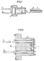
- Fig. 1 die Vorrichtung in Seitenansicht, vergröBert, mit geschnittener Hülse und geschnittenem zylindrischem Stift und
- Fig. 2 ebenfalls in Seitenansicht und besonders stark vergrößert den Diodensockel.
- Fig. 1 shows the device in side view, enlarged, with cut sleeve and cut cylindrical pin and
- Fig. 2 also in side view and particularly greatly enlarged the diode base.
Im einzelnen ist den Figuren zu entnehmen, daß ein aus einem Metallkörper bestehender Diodensockel 2 vorgesehen ist, der einen zylindrischen Außenabschnitt 14 aufweist, der mit großer Präzision hergestellt worden ist. An einer rechtwinklig zu dem Außenabschnitt 14 verlaufenden Stirnseite 15 des Diodensockels 2 ist eine von einem Rand 16 des Diodensockels umgebene zylindrische Vertiefung 12 vorgesehen. In dieser Vertiefung 12 ist eine bei Stromdurchgang infrarotes Licht emittierende Diode vom Burrus-Typ angeordnet. Der Diodenkörper ist an einem 150 µ dicken Isolierstoffplättchen 9 fixiert, z.B. mit diesem verlötet, das seinerseits am Boden 17 der Vertiefung 12 befestigt z.B. verlötet ist. Das "PlattcKen kann vorteilhaft aus Berillium- oder Aluminiumoxid oder auch aus Silizium bestehen, das außen mit einer Siliziumdioxidschicht überzogen ist. Die Diode 1 ist dadurch gegenüber dem Metallkörper des Diodensockels 2 isoliert.It can be seen in detail from the figures that a diode base 2 consisting of a metal body is provided, which has a cylindrical
Die Befestigung der Di∞e 1 an dem Diodensockel muß._so erfolgen, daß ihre lichtemittierende Fläche 13 rechtwinklig zur Achse 18 des zylindrischen Außenabschnittes 14 des Diodensockels 2 gerichtet ist und die Achse 18 durch die Mitte der Fläche 13 verläuft. Parallel zur Achse sind im Sockel 2 zwei Bohrungen 19 vorgesehen. In diesen Bohrungen 19 sind Anschlußstifte 11 isoliert befestigt, die in die Vertiefung 12 des Diodensockels 2 hineinragen und auf der anderen Seite des- Sockels 2 aus diesem vorstehen.The attachment of the Di∞e 1 to the diode base muss._so take place that its light-emitting
Über Bond-Drähte 10 ist die Anode und die Kathode der Diode 1 jeweils mit einer Stirnseite der Anschlußstifte 11 verbunden , wobei einer dieser Drähte auf der vom Scckel 2 abgewandten Oberfläche der Diode 1 fixiert ist. Der die Vertiefung 12 umgebende Rand 16 des Sockels 2 ist so bemessen, daß er zumindest mit diesem Bond-Draht bündig ist. Die Vertiefung 12 ist mit einem Epoxydharz ausgegossen, wobei das Epoxydharz die lichtemittierende Fläche 13 der Diode 1 max. mit einer Schichtdicke von 100 µ überdeckt. Das Epoxydharz mit einem Brechungsindex von ca. 1,4 bildet dadurch.einen guten Übergang zwischen dem Brechungsindex von ca. 3,5 des Diodenkörpers und dem Brechungsindex von ca. 1 für die zwischen der Diode und der Stirnseite der Glasfaser befindliche Luftstrecke.The anode and the cathode of the diode 1 are each connected to an end face of the connecting pins 11 via
Zur Verbindung des Lichtwellenleiters 6, dessen Durchmesser eher größer ist, als der Durchmesser oder die Diagonale der lichtemittierenden Fläche 13 der Diode 1, mit der Diode 1,ist eine hohlzylindrische Koppelhülse 3 vorgesehen, deren Innenraum 4 auf einer Seite der Hülse genau dem zylindrischen Außenabschnitt 14 des Diodensockels 2 angepaßt ist. Die andere Öffnung der Hülse 3 ist genau auf einen zylindrischen Stift 5 abgestimmt, in dem konzentrisch zum zylindrischen Mantel 20 des Stiftes 5 ein Endabschnitt des aus einer Einzelglasfaser bestehenden Lichtwellenleiters 6 derart fixiert ist, daß die Stirnseite des Lichtwellenleiters mit der Hülsenstirn 7 bündig ist.A hollow cylindrical coupling sleeve 3 is used to connect the optical waveguide 6, the diameter of which is larger than the diameter or the diagonal of the light-emitting
Wird der Diodensockel 2 mit seiner Stirnseite 15 zur Koppelhülse 3 gerichtet,in den Teil des Hülseninnenraumes 4 eingesetzt, der dem zylindrischen Außenabschnitt 14 des Sockels angepaßt ist, so ist damit die lichtemittierende Fläche 13 der Diode exakt auf die Achse 21 der Koppelhülse 3 ausgerichtet. In gleicher Weise wird der Lichtwellenleiter-6 auf diese Achse 21 zentriert, wenn der Stift 5 in den Teil des Hülseninnenraumes 4 eingeschoben wird, der auf den Mantel 20 des Stiftes 5 abgestimmt ist.If the diode base 2 is directed with its
Somit werden aber Lichtwellenleiter 6 und Diode 1, bzw. deren lichtemittierende Fläche 13, über die Koppelhülse . 3 aufeinander zwangsjustiert und dadurch eine optimale Einkopplung des von der Diode 1 abgestrahlten Infrarotlichtes in den Lichtwellenleiter 6 gewährleistet, ohne daß es hierzu erforderlich ist, z.B. die lichtemittierende Diode 1 zu aktivieren und an den Lichtwellenleiter 6 ein Meßgerät anzuschließen und durch Positionsänderungen der Diode gegenüber der Stirnseite des Lichtwellenleiters 6 die optimale Position der Diode gegenüber dem Lichtwellenleiter 6 herauszufinden und zu fixieren.Thus, however, optical waveguide 6 and diode 1, or their light-emitting
Der Epoxydharzkörper, der die Vertiefung 12 ausfüllt, stellt darüber hinaus sicher, daß die lichtemittierende Fläche 13 der Diode 1 und die Stirnseite des Lichtwellenleiters 6, in die das Diodenlicht einzukoppeln ist, in Richtung der Achse 21 optimal beabstandet sind, da der zylindrische Stift 5 mit dem Lichtwellenleiter 6 nur so weit in den Innenraum 4 der Koppelhülse eingeschoben werden kann, bis die Stirnseite 7 des Stiftes 5 an dem Epoxydharzkörper zur Anlage kommt.The epoxy resin body that fills the recess 12 also ensures that the
Auf der von der Diode 1 abgewandten Seite ist der Sockel 2 mit einem Flansch 22 versehen. Der Flansch 22 bildet einen Anschlag beim Einsetzen des Diodensockels 2 in den Innenraum 4 der Hülse 3. Ein dabei über den Flansch 22 überstehender Hülsenrand8 hält als Bördelrand den Diodensockel 2 in der Hülse 3 fest.On the side facing away from the diode 1, the base 2 is provided with a
Der Stift 5 kann vorteilhaft Bestandteil einer Lichtwellenleitersteckverbindung sein und durch eine an dem Lichtwellenleitersteckverbindungsteil, der den Stift 5 enthält, drehbar befestigte Überwurfmutter, die mit der Hülse 3 verschraubt werden kann in der Hülse 3 festgelegt werden.The pin 5 can advantageously be part of an optical waveguide connector and can be fixed in the sleeve 3 by means of a union nut which is rotatably fastened to the optical waveguide connector part and contains the pin 5 and can be screwed to the sleeve 3.
- 1 Diode1 diode
- 2 Diodensockel2 diode bases
- 3 Koppelhülse3 coupling sleeve
- 4 Hülseainnenraum4 sleeve interior
- 5 zylindrischer Stift5 cylindrical pin
- 6 Lichtwellenleiter-Einzelglasfaser6 single optical fiber
- 7 Stirnseite des Stiftes 57 end face of the pin 5
- 8 überstehender Bördelrand8 overhanging flange
- 9 Isolierstoffplättchen9 insulating plates
- 10 Bond-Drähte10 bond wires
- 11 Anschlußstifte11 pins
- 12 Vertiefung im Diodensockel12 recess in the diode base
- 13 lichtemittierende Fläche der Diode 113 light-emitting surface of the diode 1
- 14 zylindrischer Außenabschnitt des Diodensockels 1 4 cylindrical outer section of the diode base
- 15 Stirnseite des Diodensockels15 front side of the diode base
- 16 Rand des Diodensockels16 edge of the diode base
- 17 Boden der Vertiefung17 bottom of the recess
- 18 Achse des Diodensockels18 axis of the diode base
- 19 Sockelbohrungen19 base holes
- 20 Außenmantel des Stiftes 520 outer jacket of the pin 5
- 21 Achse der Koppelhülse 321 axis of the coupling sleeve 3
- 22 Sockelflansch22 base flange
Claims (5)
Applications Claiming Priority (2)
| Application Number | Priority Date | Filing Date | Title |
|---|---|---|---|
| DE3003331 | 1980-01-30 | ||
| DE19803003331 DE3003331A1 (en) | 1980-01-30 | 1980-01-30 | DEVICE FOR COUPLING AN INFRARED DIODE WITH AN INDIVIDUAL GLASS FIBER USED AS LIGHT WAVE GUIDE |
Publications (2)
| Publication Number | Publication Date |
|---|---|
| EP0033474A2 true EP0033474A2 (en) | 1981-08-12 |
| EP0033474A3 EP0033474A3 (en) | 1981-09-02 |
Family
ID=6093288
Family Applications (1)
| Application Number | Title | Priority Date | Filing Date |
|---|---|---|---|
| EP81100400A Ceased EP0033474A3 (en) | 1980-01-30 | 1981-01-20 | Coupling device between a diode emitting ir and a single glass-fibre used as a light wave guide |
Country Status (2)
| Country | Link |
|---|---|
| EP (1) | EP0033474A3 (en) |
| DE (1) | DE3003331A1 (en) |
Cited By (3)
| Publication number | Priority date | Publication date | Assignee | Title |
|---|---|---|---|---|
| FR2562271A1 (en) * | 1984-03-29 | 1985-10-04 | Telecommunications Sa | CONNECTOR OF AN OPTICAL FIBER AND A PHOTO-ELEMENT, RECEIVER OR TRANSMITTER, AND POSITIONING METHOD THEREOF |
| EP0854523A2 (en) * | 1997-01-15 | 1998-07-22 | Toshiba Corporation | Semiconductor light emitting device and its manufacturing method |
| EP0992820A2 (en) * | 1998-10-08 | 2000-04-12 | Samsung Electronics Co., Ltd. | Optical fibre connector module |
Families Citing this family (3)
| Publication number | Priority date | Publication date | Assignee | Title |
|---|---|---|---|---|
| DE3121870A1 (en) * | 1980-01-30 | 1982-12-23 | Siemens AG, 1000 Berlin und 8000 München | Device for coupling an infrared diode to an individual glass fibre used as an optical waveguide |
| DE19901474A1 (en) * | 1999-01-15 | 2000-07-20 | Delphi Tech Inc | Optical fiber connector |
| US20050063648A1 (en) * | 2003-09-19 | 2005-03-24 | Wilson Robert Edward | Alignment post for optical subassemblies made with cylindrical rods, tubes, spheres, or similar features |
Citations (1)
| Publication number | Priority date | Publication date | Assignee | Title |
|---|---|---|---|---|
| DE2922949A1 (en) * | 1978-06-06 | 1980-01-10 | Nippon Electric Co | DEVICE FOR CONNECTING AT LEAST ONE LIGHT-EMITTING DIODE TO AN OPTICAL LIGHT-GUIDE |
-
1980
- 1980-01-30 DE DE19803003331 patent/DE3003331A1/en not_active Ceased
-
1981
- 1981-01-20 EP EP81100400A patent/EP0033474A3/en not_active Ceased
Patent Citations (1)
| Publication number | Priority date | Publication date | Assignee | Title |
|---|---|---|---|---|
| DE2922949A1 (en) * | 1978-06-06 | 1980-01-10 | Nippon Electric Co | DEVICE FOR CONNECTING AT LEAST ONE LIGHT-EMITTING DIODE TO AN OPTICAL LIGHT-GUIDE |
Non-Patent Citations (1)
| Title |
|---|
| RESEARCH DISCLOSURE, Nr. 179, Marz 1979, Seite 108, Nr. 17910 Havant-Hants, G.B. "Connection of a photo-electric component and a light pipe". * |
Cited By (7)
| Publication number | Priority date | Publication date | Assignee | Title |
|---|---|---|---|---|
| FR2562271A1 (en) * | 1984-03-29 | 1985-10-04 | Telecommunications Sa | CONNECTOR OF AN OPTICAL FIBER AND A PHOTO-ELEMENT, RECEIVER OR TRANSMITTER, AND POSITIONING METHOD THEREOF |
| EP0854523A2 (en) * | 1997-01-15 | 1998-07-22 | Toshiba Corporation | Semiconductor light emitting device and its manufacturing method |
| EP0854523A3 (en) * | 1997-01-15 | 2000-05-10 | Kabushiki Kaisha Toshiba | Semiconductor light emitting device and its manufacturing method |
| US6274890B1 (en) | 1997-01-15 | 2001-08-14 | Kabushiki Kaisha Toshiba | Semiconductor light emitting device and its manufacturing method |
| EP0992820A2 (en) * | 1998-10-08 | 2000-04-12 | Samsung Electronics Co., Ltd. | Optical fibre connector module |
| EP0992820A3 (en) * | 1998-10-08 | 2002-06-05 | Samsung Electronics Co., Ltd. | Optical fibre connector module |
| EP1528416A1 (en) * | 1998-10-08 | 2005-05-04 | Samsung Electronics Co., Ltd. | Optical fibre connector module |
Also Published As
| Publication number | Publication date |
|---|---|
| DE3003331A1 (en) | 1981-08-06 |
| EP0033474A3 (en) | 1981-09-02 |
Similar Documents
| Publication | Publication Date | Title |
|---|---|---|
| DE2807375A1 (en) | OPTICAL COUPLING ARRANGEMENT | |
| EP0111264B1 (en) | Transmitting or receiving apparatus for opto-electrical communication equipment | |
| EP1088378B1 (en) | Housing arrangement for a laser module | |
| DE10065624C2 (en) | Coupling arrangement for optically coupling an optical waveguide to an electro-optical or opto-electrical semiconductor converter | |
| DE69837236T2 (en) | OPTICAL MODULE | |
| DE3822312C2 (en) | ||
| DE19932430C2 (en) | Opto-electronic assembly and component for this assembly | |
| DE3043613A1 (en) | COATING FOR A PHOTODIOD | |
| DE3732433A1 (en) | LASER MODULE AND METHOD FOR COUPLING A GLASS FIBER | |
| EP0078364A2 (en) | Opto-electronic coupling device | |
| EP0361153A2 (en) | Arrangement for coupling an optical fibre with a coupling window of a planar integrated optical device, and method for making such an arrangement | |
| DE2829548A1 (en) | CARRIER FOR A LIGHT EMITTING DEVICE | |
| DE2922949A1 (en) | DEVICE FOR CONNECTING AT LEAST ONE LIGHT-EMITTING DIODE TO AN OPTICAL LIGHT-GUIDE | |
| DE10004411A1 (en) | Electro-optical transmitter / receiver module and method for its production | |
| EP0111263A2 (en) | Transmitting or receiving apparatus containing a diode in a support | |
| EP1101136B1 (en) | Optoelectronic transceiver | |
| DE2913262A1 (en) | ELECTRO-OPTICAL CONNECTING DEVICE | |
| EP0175936B1 (en) | Opto-electronic device | |
| EP0833764B1 (en) | Device for detecting the level of humidity on a pane | |
| EP0033474A2 (en) | Coupling device between a diode emitting IR and a single glass-fibre used as a light wave guide | |
| WO1995000283A1 (en) | Process and device for connecting a contact element | |
| DE60222736T2 (en) | Optical module with monitor photodiode | |
| EP0207373A1 (en) | Ferrule for an optical wave guide | |
| EP0622874A1 (en) | Arrangement for coupling an opto-electronic receiving element to an opto-electronic transmitting element | |
| DE8002368U1 (en) | DEVICE FOR COUPLING AN INFRARED DIODE WITH AN INDIVIDUAL GLASS FIBER USED AS LIGHT WAVE GUIDE |
Legal Events
| Date | Code | Title | Description |
|---|---|---|---|
| PUAI | Public reference made under article 153(3) epc to a published international application that has entered the european phase |
Free format text: ORIGINAL CODE: 0009012 |
|
| PUAL | Search report despatched |
Free format text: ORIGINAL CODE: 0009013 |
|
| AK | Designated contracting states |
Designated state(s): AT BE CH DE FR GB IT NL SE |
|
| AK | Designated contracting states |
Designated state(s): AT BE CH DE FR GB IT NL SE |
|
| 17P | Request for examination filed |
Effective date: 19810826 |
|
| STAA | Information on the status of an ep patent application or granted ep patent |
Free format text: STATUS: THE APPLICATION HAS BEEN REFUSED |
|
| 18R | Application refused |
Effective date: 19830421 |
|
| RIN1 | Information on inventor provided before grant (corrected) |
Inventor name: PLIHAL, MANFRED, DR. DIPL.-PHYS. Inventor name: GOERNE, JAN, DIPL.-ING. |