EP0033474A2 - Dispositif de couplage d'une diode luminescente infrarouge avec comme guide de lumière une fibre de verre unique - Google Patents
Dispositif de couplage d'une diode luminescente infrarouge avec comme guide de lumière une fibre de verre unique Download PDFInfo
- Publication number
- EP0033474A2 EP0033474A2 EP81100400A EP81100400A EP0033474A2 EP 0033474 A2 EP0033474 A2 EP 0033474A2 EP 81100400 A EP81100400 A EP 81100400A EP 81100400 A EP81100400 A EP 81100400A EP 0033474 A2 EP0033474 A2 EP 0033474A2
- Authority
- EP
- European Patent Office
- Prior art keywords
- diode
- base
- cylindrical
- light
- sleeve
- Prior art date
- Legal status (The legal status is an assumption and is not a legal conclusion. Google has not performed a legal analysis and makes no representation as to the accuracy of the status listed.)
- Ceased
Links
Images
Classifications
-
- G—PHYSICS
- G02—OPTICS
- G02B—OPTICAL ELEMENTS, SYSTEMS OR APPARATUS
- G02B6/00—Light guides; Structural details of arrangements comprising light guides and other optical elements, e.g. couplings
- G02B6/24—Coupling light guides
- G02B6/42—Coupling light guides with opto-electronic elements
- G02B6/4292—Coupling light guides with opto-electronic elements the light guide being disconnectable from the opto-electronic element, e.g. mutually self aligning arrangements
-
- H—ELECTRICITY
- H01—ELECTRIC ELEMENTS
- H01L—SEMICONDUCTOR DEVICES NOT COVERED BY CLASS H10
- H01L2924/00—Indexing scheme for arrangements or methods for connecting or disconnecting semiconductor or solid-state bodies as covered by H01L24/00
- H01L2924/0001—Technical content checked by a classifier
- H01L2924/0002—Not covered by any one of groups H01L24/00, H01L24/00 and H01L2224/00
-
- H—ELECTRICITY
- H01—ELECTRIC ELEMENTS
- H01L—SEMICONDUCTOR DEVICES NOT COVERED BY CLASS H10
- H01L33/00—Semiconductor devices with at least one potential-jump barrier or surface barrier specially adapted for light emission; Processes or apparatus specially adapted for the manufacture or treatment thereof or of parts thereof; Details thereof
- H01L33/48—Semiconductor devices with at least one potential-jump barrier or surface barrier specially adapted for light emission; Processes or apparatus specially adapted for the manufacture or treatment thereof or of parts thereof; Details thereof characterised by the semiconductor body packages
- H01L33/483—Containers
Definitions
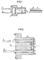
- the invention relates to a device for coupling a single optical fiber used as an optical waveguide with an infrared diode of Burrus type, in which the infrared diode at the end face of a cylindrical D i odensockels fixed and the glass fiber having an end portion in the bore of a cylindrical pin is caught and a hollow cylindrical coupling sleeve is provided, the interior of which is set up on one side for receiving the base and on the other side for receiving the pin.
- Such a device known from DE-OS 29 22 949, is required if electrical signals are to be converted into optical signals and sent over an optical transmission link. It is important that the light-emitting surface of the diode with its axis running through its center point and perpendicular to it is aligned precisely with the axis of an end section of the optical waveguide in order to keep the coupling losses as low as possible.
- the diode e.g. to be able to replace in the event of a defect without the need for complex adjustment work of this type.
- the object of the present invention is therefore to design a device of the type mentioned at the outset in such a way that no complex adjustment work for aligning the diode and optical waveguide (glass fiber) is necessary.
- this object is achieved in that the cylindrical outer portion of the diode base is formed with great precision and the diode with its light-emitting surface is fixed at right angles to this outer portion and with the center of the light-emitting surface concentric to the axis of the outer portion of the diode base and that the interior of the coupling sleeve is precisely matched on one side to the cylindrical outer section of the diode base and on the other side to the outer surface of the pin.
- the diode are pre-adjusted precisely to the outer portion of the diode base and the glass fiber accurately onto the cylindrical outer surface of the cylindrical pin, wherein in particular the adjust- r ung of the diode can be passive, ie without the diode to emit light must be excited, glass fiber and diode are automatically forcibly adjusted to each other when inserted into the coupling sleeve, thus avoiding any adjustment work when coupling the diode and glass fiber.
- the diode is made of berillium or aluminum oxide or at least on the outside of which plates made of silicon dioxide are fastened, which is fixed to the bottom of a depression which is worked into the end face of the diode base,
- the depression is filled with epoxy resin and that the light-emitting surface of the diode is covered by an epoxy resin layer with a max. Thickness of 100 microns is covered, or that the recess is covered by a glass plate connected to the edge of the recess and that the diode base is fixed in the sleeve by flanging a sleeve edge protruding over the inserted diode base.
- a diode base 2 consisting of a metal body is provided, which has a cylindrical outer section 14 which has been manufactured with great precision.
- a Burrus-type diode emitting infrared light when current is passed is arranged in this recess 12.
- the diode body is fixed to a 150 ⁇ m thick insulating material plate 9, for example soldered to it, which in turn is fastened, for example, soldered to the bottom 17 of the depression 12.
- the plate can advantageously consist of beryllium or aluminum oxide or also of silicon, which is coated on the outside is coated with a silicon dioxide layer.
- the diode 1 is thereby isolated from the metal body of the diode base 2.
- the anode and the cathode of the diode 1 are each connected to an end face of the connecting pins 11 via bond wires 10, one of these wires being fixed on the surface of the diode 1 facing away from the scanner 2.
- the edge 16 of the base 2 surrounding the recess 12 is dimensioned such that it is at least flush with this bond wire.
- the depression 12 is cast with an epoxy resin, the epoxy resin making the light-emitting surface 13 of the diode 1 max. covered with a layer thickness of 100 ⁇ .
- the epoxy resin with a refractive index of approximately 1.4 thus forms a good transition between the refractive index of approximately 3.5 of the diode body and the refractive index of approximately 1 for the air gap between the diode and the end face of the glass fiber.
- a hollow cylindrical coupling sleeve 3 is used to connect the optical waveguide 6, the diameter of which is larger than the diameter or the diagonal of the light-emitting surface 13 of the diode 1, to the diode 1 provided, the interior 4 on one side of the sleeve is exactly adapted to the cylindrical outer portion 14 of the diode base 2.
- the other opening of the sleeve 3 is precisely matched to a cylindrical pin 5, in which an end portion of the optical fiber 6 consisting of a single glass fiber 6 is fixed concentrically to the cylindrical jacket 20 of the pin 5 such that the end face of the optical fiber is flush with the sleeve face 7.
- the diode base 2 is directed with its end face 15 towards the coupling sleeve 3, inserted into the part of the sleeve interior 4 which is adapted to the cylindrical outer section 14 of the base, the light-emitting surface 13 of the diode is thus exactly aligned with the axis 21 of the coupling sleeve 3.
- the optical waveguide 6 is centered on this axis 21 when the pin 5 is inserted into the part of the sleeve interior 4 which is matched to the jacket 20 of the pin 5.
- the epoxy resin body that fills the recess 12 also ensures that the light emitting Surface 13 of the diode 1 and the end face of the optical waveguide 6, into which the diode light is to be coupled, are optimally spaced in the direction of the axis 21, since the cylindrical pin 5 with the optical waveguide 6 can only be inserted as far into the interior 4 of the coupling sleeve, until the end face 7 of the pin 5 comes into contact with the epoxy resin body.
- the base 2 On the side facing away from the diode 1, the base 2 is provided with a flange 22.
- the flange 22 forms a stop when the diode base 2 is inserted into the interior 4 of the sleeve 3.
- a sleeve edge 8 projecting beyond the flange 22 holds the diode base 2 in the sleeve 3 as a flanged edge.
- the pin 5 can advantageously be part of an optical waveguide connector and can be fixed in the sleeve 3 by means of a union nut which is rotatably fastened to the optical waveguide connector part and contains the pin 5 and can be screwed to the sleeve 3.
Applications Claiming Priority (2)
| Application Number | Priority Date | Filing Date | Title |
|---|---|---|---|
| DE3003331 | 1980-01-30 | ||
| DE19803003331 DE3003331A1 (de) | 1980-01-30 | 1980-01-30 | Vorrichtung zur kopplung einer infrarotdiode mit einer als lichtwellenleiter verwendeten einzelglasfaser |
Publications (2)
| Publication Number | Publication Date |
|---|---|
| EP0033474A2 true EP0033474A2 (fr) | 1981-08-12 |
| EP0033474A3 EP0033474A3 (fr) | 1981-09-02 |
Family
ID=6093288
Family Applications (1)
| Application Number | Title | Priority Date | Filing Date |
|---|---|---|---|
| EP81100400A Ceased EP0033474A3 (fr) | 1980-01-30 | 1981-01-20 | Dispositif de couplage d'une diode luminescente infrarouge avec comme guide de lumière une fibre de verre unique |
Country Status (2)
| Country | Link |
|---|---|
| EP (1) | EP0033474A3 (fr) |
| DE (1) | DE3003331A1 (fr) |
Cited By (3)
| Publication number | Priority date | Publication date | Assignee | Title |
|---|---|---|---|---|
| FR2562271A1 (fr) * | 1984-03-29 | 1985-10-04 | Telecommunications Sa | Connecteur d'une fibre optique et d'un photo-element, recepteur ou emetteur, et procede de positionnement de ceux-ci |
| EP0854523A2 (fr) * | 1997-01-15 | 1998-07-22 | Toshiba Corporation | Dispositif semi-conducteur émetteur de lumière et méthode de fabrication |
| EP0992820A2 (fr) * | 1998-10-08 | 2000-04-12 | Samsung Electronics Co., Ltd. | Module de connecteur à fibre optique |
Families Citing this family (3)
| Publication number | Priority date | Publication date | Assignee | Title |
|---|---|---|---|---|
| DE3121870A1 (de) * | 1980-01-30 | 1982-12-23 | Siemens AG, 1000 Berlin und 8000 München | Vorrichtung zur kopplung einer infrarotdiode mit einer als lichtwellenleiter verwendeten einzelglasfaser |
| DE19901474A1 (de) * | 1999-01-15 | 2000-07-20 | Delphi Tech Inc | Lichtleitfaser-Steckverbinder |
| US20050063648A1 (en) * | 2003-09-19 | 2005-03-24 | Wilson Robert Edward | Alignment post for optical subassemblies made with cylindrical rods, tubes, spheres, or similar features |
Citations (1)
| Publication number | Priority date | Publication date | Assignee | Title |
|---|---|---|---|---|
| DE2922949A1 (de) * | 1978-06-06 | 1980-01-10 | Nippon Electric Co | Vorrichtung zum anschluss wenigstens einer licht emittierenden diode an einen optischen lichtleiter |
-
1980
- 1980-01-30 DE DE19803003331 patent/DE3003331A1/de not_active Ceased
-
1981
- 1981-01-20 EP EP81100400A patent/EP0033474A3/fr not_active Ceased
Patent Citations (1)
| Publication number | Priority date | Publication date | Assignee | Title |
|---|---|---|---|---|
| DE2922949A1 (de) * | 1978-06-06 | 1980-01-10 | Nippon Electric Co | Vorrichtung zum anschluss wenigstens einer licht emittierenden diode an einen optischen lichtleiter |
Non-Patent Citations (1)
| Title |
|---|
| RESEARCH DISCLOSURE, Nr. 179, Marz 1979, Seite 108, Nr. 17910 Havant-Hants, G.B. "Connection of a photo-electric component and a light pipe". * |
Cited By (7)
| Publication number | Priority date | Publication date | Assignee | Title |
|---|---|---|---|---|
| FR2562271A1 (fr) * | 1984-03-29 | 1985-10-04 | Telecommunications Sa | Connecteur d'une fibre optique et d'un photo-element, recepteur ou emetteur, et procede de positionnement de ceux-ci |
| EP0854523A2 (fr) * | 1997-01-15 | 1998-07-22 | Toshiba Corporation | Dispositif semi-conducteur émetteur de lumière et méthode de fabrication |
| EP0854523A3 (fr) * | 1997-01-15 | 2000-05-10 | Kabushiki Kaisha Toshiba | Dispositif semi-conducteur émetteur de lumière et méthode de fabrication |
| US6274890B1 (en) | 1997-01-15 | 2001-08-14 | Kabushiki Kaisha Toshiba | Semiconductor light emitting device and its manufacturing method |
| EP0992820A2 (fr) * | 1998-10-08 | 2000-04-12 | Samsung Electronics Co., Ltd. | Module de connecteur à fibre optique |
| EP0992820A3 (fr) * | 1998-10-08 | 2002-06-05 | Samsung Electronics Co., Ltd. | Module de connecteur à fibre optique |
| EP1528416A1 (fr) * | 1998-10-08 | 2005-05-04 | Samsung Electronics Co., Ltd. | Module de connecteur à fibre optique |
Also Published As
| Publication number | Publication date |
|---|---|
| DE3003331A1 (de) | 1981-08-06 |
| EP0033474A3 (fr) | 1981-09-02 |
Similar Documents
| Publication | Publication Date | Title |
|---|---|---|
| DE2807375A1 (de) | Optische kopplungsanordnung | |
| EP0111264B1 (fr) | Appareil de transmission ou réception pour équipement opto-électrique de communication | |
| EP1088378B1 (fr) | Ensemble boitier pour module laser | |
| DE10065624C2 (de) | Kopplungsanordnung zum optischen Koppeln eines Lichtwellenleiters mit einem elektro-optischen oder opto-elektrischen Halbleiterwandler | |
| DE69837236T2 (de) | Optisches modul | |
| DE3822312C2 (fr) | ||
| DE19932430C2 (de) | Opto-elektronische Baugruppe sowie Bauteil für diese Baugruppe | |
| DE3043613A1 (de) | Umhuellung fuer eine photodiode | |
| DE3732433A1 (de) | Lasermodul und verfahren zum ankoppeln einer glasfaser | |
| EP0078364A2 (fr) | Elément de couplage opto-électronique | |
| EP1174745A2 (fr) | Module optoélectronique montable en surface | |
| EP0361153A2 (fr) | Dispositif pour coupler une fibre optique à une fenêtre de couplage d'un élément optique à intégration plane et sa méthode de fabrication | |
| DE2922949A1 (de) | Vorrichtung zum anschluss wenigstens einer licht emittierenden diode an einen optischen lichtleiter | |
| DE10004411A1 (de) | Elektrooptisches Sende-/Empfangsmodul und Verfahren zu seiner Herstellung | |
| EP0111263A2 (fr) | Appareil de transmission ou réception contenant une diode dans une monture | |
| DE2913262A1 (de) | Elektro-optische verbindungsvorrichtung | |
| EP0175936B1 (fr) | Appareil opto-électronique | |
| EP0833764B1 (fr) | Dispositif de detection du niveau d'humidite sur une vitre | |
| EP0033474A2 (fr) | Dispositif de couplage d'une diode luminescente infrarouge avec comme guide de lumière une fibre de verre unique | |
| WO2000007052A1 (fr) | Unite d'emission et de reception optoelectronique | |
| WO1995000283A1 (fr) | Procede et dispositif de connexion d'un element de contact | |
| EP0207373A1 (fr) | Embout pour guide d'onde optique | |
| EP0622874A1 (fr) | Arrangement de couplage entre un élément optoélectronique récepteur et un élément optoélectronique émetteur | |
| DE3413749C2 (fr) | ||
| DE19622459C1 (de) | Elektrooptisches Modul |
Legal Events
| Date | Code | Title | Description |
|---|---|---|---|
| PUAI | Public reference made under article 153(3) epc to a published international application that has entered the european phase |
Free format text: ORIGINAL CODE: 0009012 |
|
| PUAL | Search report despatched |
Free format text: ORIGINAL CODE: 0009013 |
|
| AK | Designated contracting states |
Designated state(s): AT BE CH DE FR GB IT NL SE |
|
| AK | Designated contracting states |
Designated state(s): AT BE CH DE FR GB IT NL SE |
|
| 17P | Request for examination filed |
Effective date: 19810826 |
|
| STAA | Information on the status of an ep patent application or granted ep patent |
Free format text: STATUS: THE APPLICATION HAS BEEN REFUSED |
|
| 18R | Application refused |
Effective date: 19830421 |
|
| RIN1 | Information on inventor provided before grant (corrected) |
Inventor name: PLIHAL, MANFRED, DR. DIPL.-PHYS. Inventor name: GOERNE, JAN, DIPL.-ING. |