EP0110317A2 - Small power consumption circuit for driving high-speed digital-signal transmission lines - Google Patents
Small power consumption circuit for driving high-speed digital-signal transmission lines Download PDFInfo
- Publication number
- EP0110317A2 EP0110317A2 EP83111724A EP83111724A EP0110317A2 EP 0110317 A2 EP0110317 A2 EP 0110317A2 EP 83111724 A EP83111724 A EP 83111724A EP 83111724 A EP83111724 A EP 83111724A EP 0110317 A2 EP0110317 A2 EP 0110317A2
- Authority
- EP
- European Patent Office
- Prior art keywords
- transistors
- transistor
- emitters
- generator
- current
- Prior art date
- Legal status (The legal status is an assumption and is not a legal conclusion. Google has not performed a legal analysis and makes no representation as to the accuracy of the status listed.)
- Granted
Links
Images


Classifications
-
- H—ELECTRICITY
- H03—ELECTRONIC CIRCUITRY
- H03K—PULSE TECHNIQUE
- H03K19/00—Logic circuits, i.e. having at least two inputs acting on one output; Inverting circuits
- H03K19/0175—Coupling arrangements; Interface arrangements
- H03K19/018—Coupling arrangements; Interface arrangements using bipolar transistors only
- H03K19/01825—Coupling arrangements, impedance matching circuits
- H03K19/01831—Coupling arrangements, impedance matching circuits with at least one differential stage
-
- H—ELECTRICITY
- H03—ELECTRONIC CIRCUITRY
- H03K—PULSE TECHNIQUE
- H03K19/00—Logic circuits, i.e. having at least two inputs acting on one output; Inverting circuits
- H03K19/0008—Arrangements for reducing power consumption
- H03K19/001—Arrangements for reducing power consumption in bipolar transistor circuits
Definitions
- the present invention concerns high-speed digital-signal transmission circuits and in particular it provides a small power consumption circuit for driving transmission lines for digital signals at ECL logic levels.
- ECL driving circuits comprise a differential input stage and an output stage comprising a pair of common collector transistors the emitters of which supply , at the circuit output both the high and the low logic level signals (balanced output).
- Such transistors are connected each to a bias current source (a current generator or a resistor) which supplies a constant current, high enough to prevent the transistors from being cut off even when they send a low-level signal on the line, i. e. when the transistors receive current from the line instead of sending current on the line. Owing to this high bias current, the power consumption of the transistors under stationary conditions is high.
- a bias current source a current generator or a resistor
- the maximum current a transistor is to supply when transmitting signals is considerably hi gh, as such current is the sum of the signal current and the bias current, As a consequence, the transistors are to be dimensioned so as to be able to tolerate such high currents, what can also cause reliability problems.
- Power-consumption and dimensioning problems are particularly critical when the driving circuit is to be inserted into an integrated circuit, e. g. toghether with a signal transceiver.
- the aim of the present invention is to provide a driving circuit having a small power consumption under stationary conditions and allowing a reduction in the current delivered during transmission, without reducing the circuit switching speed . This is obtained by the emitters of output stages the transistors being connectable to a common bias current generator through a switching circuit, which connects the common generator to either transistor, according to which transistor is sending a signal at low logic level over the line.
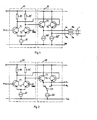
- a conventional ECL circuit for driving high-speed digital lines comprises an input differential a.tage (or switching circuit) Al as well as an output stage UI which provides two signals with opposite logic-level (balanced output).
- Input stage Al consists of two transistors Tl, T2 with collector resistors RI, R1', and of current generator Gl.
- the base of TI is connected to the signal input In and the base of T2 is connected to a voltage V BB intermediate between the voltages corresponding to high and low logic levels.
- Output stage Ul comprises two common-collector transistors T3, T4, having the bases connected to the collectors of TI, T2 and the emitters connected to the circuit outputs el, e2; these are in turn connected to a balanced line L 2 whose termination resistors are shown at R 8 .
- the emitters of T3, T4 are in turn connected to supply voltage V EE through a bias current source, here represented by current generators GO', G0", which usually are external to the circuit to allow different line driving requirements to be easily met.
- Fig.2 shows the modifications made according to the invention to the driving circuit.
- the emitters of transistors T3, T4 are connected through a switching circuit CM to a common source of bias current I0, schematized by generator G0.
- switching circuit CM connects generator GO to the transistor that at a certain instant sends the low-level signal on the line, and switches when the logic level of the signal changes, thereby connecting the generator to the other transistor.
- the switching of CM can be very fast and simultaneous with the switching of transistors T3, T4.
- Fig. 3 shows a circuit diagram of the invention, in case voltage levels to send over the line are just ECL levels.
- generator G1 has been represented in details, which generator consists of transistor T5 and resistor R2.
- the emitters of transistors T3, T4 are connected to the collectors of a pair of transistors T6, T7 of which the emitters are connected to the collector of a further transistor T8 which together with resistor R3 forms generator G0.
- the bases of T6, T7 are connected through diodes D1, D2 to the collectors of T2, T1 respectively; the cross- connection between T1, T2 and T6, T7 (i.e. the connection such that T1 drives transistor T7, connected to T4, and T2 drives transistor T6, connected to T3) allows, as will be seen hereinafter , current 10 to be supplied to the transistor which sends the low-level signal on the line.
- Diodes Dl, D2 are connected to bias resistors R4, R5 and are inserted so that they are always conducting; their task is to shift the voltage levels at the bases of transistors T6, T7 so as to ensure driving of the transistors while inhibiting their saturation and without attenuating the signal present on the collectors of Tl, T2.
- Two further current generators G2, G3, consisting respectively of transistors T9, T10 and resistors R6, R7, are connected to the emitters of T3, T4 and supply a bias current I2, which is much lower than that supplied by GO(e. g. 1 mA), so as to prevent the cut-off of T3, T4, when they are hot connected to G0.
- generator GO can be programmed at a predetermined value, by presetting the reference voltage V , applied to the basis of T8, in a manner well-known to the person killed in the art.
- T6 conducts and supplies current 10 to T3, which sends the low-level signal over the line, while T7 becomes cut off, thereby disconnecting T4 from G0.
- the output impedances are considerably low and hence the switching of T6, T7 causes no disturbances; therefore at the output there are the waveforms typical of ECL logic.
- Fig. 4 shows a variant embodiment apt to drive lines which to not require ECL logic levels, but more symmetrical levels in re- pect of supply; the elements which have already been described with reference to Fig. 3 are denoted by the same reference symbols.
- the bases of transistors T6, T7 are connected through diodes D3, D4, analogous to D1, D2, to the emit- ers of a pair of common-collector transistors Tll, T12, which drive :ransistors TI, T2.
- Diodes D3, D4 are associated with resistors R9, R3 ana- .ogous to R4, R5.
- a further diode D5 causes the level shift at the col- ectors of TI, T2.
- generators GO-G3 are not shown in details.
- the operation is then the following: by applying,for instance, a low-level signal (-1, 6 V) to In, the basis of T 1 is at about - 2, 3 V and the basis of T2, as an effect of voltage V BB applied to the base of T12, passes to - I, 9 V.
- the whole of current II passes through T2 and the collector of TI passes to a voltage corresponding to the drop across D5, i.e. - 0, 8 V.
- this arrangement ensures that no delays occur in the switching of T6, T7 with respect to T3, T4; indeed, as T6, T7 are driven by signals extracted upstream those which drive T3, T4, the switching of the latter could even be shortly delayed with respect to that of T 6, T7.
- An arrangement like that of Fig. 4 presents the advantage that it does not load the collectors of TI, T2 to drive T6, T7.
Abstract
Description
- The present invention concerns high-speed digital-signal transmission circuits and in particular it provides a small power consumption circuit for driving transmission lines for digital signals at ECL logic levels.
- It is known that conventional ECL driving circuits comprise a differential input stage and an output stage comprising a pair of common collector transistors the emitters of which supply , at the circuit output both the high and the low logic level signals (balanced output).
- Such transistors are connected each to a bias current source (a current generator or a resistor) which supplies a constant current, high enough to prevent the transistors from being cut off even when they send a low-level signal on the line, i. e. when the transistors receive current from the line instead of sending current on the line. Owing to this high bias current, the power consumption of the transistors under stationary conditions is high.
- Moreover, also the maximum current a transistor is to supply when transmitting signals is considerably hi gh, as such current is the sum of the signal current and the bias current, As a consequence, the transistors are to be dimensioned so as to be able to tolerate such high currents, what can also cause reliability problems.
- Power-consumption and dimensioning problems are particularly critical when the driving circuit is to be inserted into an integrated circuit, e. g. toghether with a signal transceiver.
- The aim of the present invention is to provide a driving circuit having a small power consumption under stationary conditions and allowing a reduction in the current delivered during transmission, without reducing the circuit switching speed . This is obtained by the emitters of output stages the transistors being connectable to a common bias current generator through a switching circuit, which connects the common generator to either transistor, according to which transistor is sending a signal at low logic level over the line.
- To make the invention more understandable, reference is made to the annexed drawings in which :
- - Fig. 1 is a schematic diagram of a conventional ECL driving circuit
- - Fig. 2 is a schematic diagram of the invention
- - Figures 3, 4 are circuit diagrams of two embodiments of the invention.
- As shown in Fig. 1, a conventional ECL circuit for driving high-speed digital lines comprises an input differential a.tage (or switching circuit) Al as well as an output stage UI which provides two signals with opposite logic-level (balanced output).
- Input stage Al consists of two transistors Tl, T2 with collector resistors RI, R1', and of current generator Gl. The base of TI is connected to the signal input In and the base of T2 is connected to a voltage VBB intermediate between the voltages corresponding to high and low logic levels.
- Output stage Ul comprises two common-collector transistors T3, T4, having the bases connected to the collectors of TI, T2 and the emitters connected to the circuit outputs el, e2; these are in turn connected to a balanced line L2 whose termination resistors are shown at R8. The emitters of T3, T4 are in turn connected to supply voltage VEE through a bias current source, here represented by current generators GO', G0", which usually are external to the circuit to allow different line driving requirements to be easily met.
- Generators G0', GO" generate a bias current I0, of such a value as to prevent the cut-off of transistors T3, T4 when they are to send a signal at low-logic level on the line, i.e. when the transistors receive current from the line. By the usual values of 10 and VEE (10 mA e 5V respectively), power consumption under stationary condi- tions, (2 I0. VEE) is of the order of 100 mW; in addition the transistor providing the high-level signal sends a current 10 + IL (with IL signal current, which too is of the order of 10 mA) on the respective line wire, also this current being rather high. This causes the disadvantages mentioned in the introductory part of the specification.
- Fig.2 , where the elements equal to those of Fig. 1 are denoted by the same references, shows the modifications made according to the invention to the driving circuit.
- These modifications have been suggested by the fact that, in a transmission over a balanced-line, when one of the two transistors sends a low-level signal on the line, the other sends the high-level signal; hence only one of the two transistors needs bias current 10.
- Therefore in the output stage U2 modified in accordance with the invention, the emitters of transistors T3, T4, are connected through a switching circuit CM to a common source of bias current I0, schematized by generator G0.
- During transmission, switching circuit CM connects generator GO to the transistor that at a certain instant sends the low-level signal on the line, and switches when the logic level of the signal changes, thereby connecting the generator to the other transistor.
- As ECL logic is used, the switching of CM can be very fast and simultaneous with the switching of transistors T3, T4.
- Fig. 3 shows a circuit diagram of the invention, in case voltage levels to send over the line are just ECL levels. As to input amplifier Al, generator G1 has been represented in details, which generator consists of transistor T5 and resistor R2. In output stage U2, the emitters of transistors T3, T4 are connected to the collectors of a pair of transistors T6, T7 of which the emitters are connected to the collector of a further transistor T8 which together with resistor R3 forms generator G0. The bases of T6, T7 are connected through diodes D1, D2 to the collectors of T2, T1 respectively; the cross- connection between T1, T2 and T6, T7 (i.e. the connection such that T1 drives transistor T7, connected to T4, and T2 drives transistor T6, connected to T3) allows, as will be seen hereinafter , current 10 to be supplied to the transistor which sends the low-level signal on the line.
- Diodes Dl, D2 are connected to bias resistors R4, R5 and are inserted so that they are always conducting; their task is to shift the voltage levels at the bases of transistors T6, T7 so as to ensure driving of the transistors while inhibiting their saturation and without attenuating the signal present on the collectors of Tl, T2. Two further current generators G2, G3, consisting respectively of transistors T9, T10 and resistors R6, R7, are connected to the emitters of T3, T4 and supply a bias current I2, which is much lower than that supplied by GO(e. g. 1 mA), so as to prevent the cut-off of T3, T4, when they are hot connected to G0. To allow different driving requirements (different line impedances, different operating speeds, and so on) to be met, generator GO can be programmed at a predetermined value, by presetting the reference voltage V , applied to the basis of T8, in a manner well-known to the person killed in the art.
- The operation of the circuit of Fig. 3 will now be described supposing that generators G1, G2, G3 supply a current of the order of 1 mA, that the resistance of R1, R1' is of the order of 800 Ω and the voltage values are - 0, 8 V for the high logic level, -I, 6 V for the low logic level and - 1, 2 V for VBB. By supposing that a signal at low level is presentIn, current Il supplied by GI passes through transistor T2, while T1 is cut-off.
- As a consequence the collector of Tl and hence the basis of T3 are substantially grounded, while the collector of T2 and the basis of T4 are at - 0, 8 V.
- Voltages of -0, 8 V (high level) and - 1, 6 V (low level) will be present at the emitters of T3, T4 respectively and hence at outputs el, e2 towards the line to be driven . Under the assumption of a voltage drop across diodes Dl, D2 of the order of 0, 7 V, the basis of T6 passes to - 1, 5 V and the basis of T7 to - 0, 7 V. T6 is then cut off, and the current supplied by GO passes through transistor T7 and is supplied to T4, which sends the low-level signal over the line.
- When the signal at input In becomes high, the situation is reversed; T6 conducts and supplies current 10 to T3, which sends the low-level signal over the line, while T7 becomes cut off, thereby disconnecting T4 from G0.
- For a correct circuit operation the switching of transistors T6, T7 must be substantially simultaneous with that of T3, T4. In the circuit shown, this is certainly obtained, since T3, T4 and T6, T7 are driven by the same signal, as diodes Dl, D2 are always conducting.
- In addition, when the circuit is unloaded, the output impedances (impedances presented by the transistors as viewed from the emitters) are considerably low and hence the switching of T6, T7 causes no disturbances; therefore at the output there are the waveforms typical of ECL logic.
- In addition,due to the balanced arrangement of transistors T6, T7, thermal drifts (as those of diodes Dl, D2) are compensated for and do not affect the output signals.
- By this arrangement the drawbacks due to high power consumption and high current to be delivered are clearly eliminated. In fact under stationary conditions the power consumption will be (I0+2·I2)·VEE i. e. , with the above - mentioned values , 60 mW instead of 00 mW as in the prior art circuit; the current delivered by the tran- istor which sends the high-level signal will be IL +12, i.e. about I mA instead of 20 mA. Maximum current at the output transistors s .nd power consumption are substantially halved.
- Fig. 4 shows a variant embodiment apt to drive lines which to not require ECL logic levels, but more symmetrical levels in re- pect of supply; the elements which have already been described with reference to Fig. 3 are denoted by the same reference symbols.
- In this variant embodiment, the bases of transistors T6, T7 are connected through diodes D3, D4, analogous to D1, D2, to the emit- ers of a pair of common-collector transistors Tll, T12, which drive :ransistors TI, T2.
- Diodes D3, D4 are associated with resistors R9, R3 ana- .ogous to R4, R5. A further diode D5 causes the level shift at the col- ectors of TI, T2. To make the drawing simpler, generators GO-G3 are not shown in details.
- To describe the operation of the circuit of Fig. 4 it will be supposed that - 1, 6 V and - 2, 4 V voltages are desired at outputs e1, e2, for the high and the low level respectively; diode D5 is then to cause a voltage drop of about 0, 8 V to give the corresponding level shift with respect to ECL levels.
- The operation is then the following: by applying,for instance, a low-level signal (-1, 6 V) to In, the basis of T 1 is at about - 2, 3 V and the basis of T2, as an effect of voltage VBB applied to the base of T12, passes to - I, 9 V. The whole of current II passes through T2 and the collector of TI passes to a voltage corresponding to the drop across D5, i.e. - 0, 8 V.
- As in the circuit of Fig. 3, low and high levels will be present at outputs e2, e1 respectively, such levels being respectively in this case - I, 6 V and - 2, 4 V.
- Under the described conditions, and taking into account the voltage drops across D3, D4 (whichare supposed to be equal to those across Dl, D2) the basis of T6 passes to -3 V and that of T7 to - 2, 6 V, hence current 1.0 passes through T7 and is supplied to transistor T4 which emits the low level signal.
- With a high level signal the situation reverses; with respect to the diagram of Fig. 3 there is the difference that the voltage at the base of T7 remains unchanged, as it depends on voltage V BB which is constant, while the voltage at the base of T6 passes to - 2, 2 V.
- Also this arrangement ensures that no delays occur in the switching of T6, T7 with respect to T3, T4; indeed, as T6, T7 are driven by signals extracted upstream those which drive T3, T4, the switching of the latter could even be shortly delayed with respect to that of T 6, T7.
- An arrangement like that of Fig. 4 presents the advantage that it does not load the collectors of TI, T2 to drive T6, T7.
Claims (5)
Applications Claiming Priority (2)
| Application Number | Priority Date | Filing Date | Title |
|---|---|---|---|
| IT68364/82A IT1157089B (en) | 1982-11-24 | 1982-11-24 | LOW DISSIPATION CIRCUIT FOR DRIVING HIGH SPEED NUMBER SIGNAL TRANSMISSION LINES |
| IT6836482 | 1982-11-24 |
Publications (3)
| Publication Number | Publication Date |
|---|---|
| EP0110317A2 true EP0110317A2 (en) | 1984-06-13 |
| EP0110317A3 EP0110317A3 (en) | 1985-08-14 |
| EP0110317B1 EP0110317B1 (en) | 1989-03-29 |
Family
ID=11309139
Family Applications (1)
| Application Number | Title | Priority Date | Filing Date |
|---|---|---|---|
| EP83111724A Expired EP0110317B1 (en) | 1982-11-24 | 1983-11-23 | Small power consumption circuit for driving high-speed digital-signal transmission lines |
Country Status (6)
| Country | Link |
|---|---|
| US (1) | US4593211A (en) |
| EP (1) | EP0110317B1 (en) |
| JP (1) | JPS59146227A (en) |
| CA (1) | CA1226045A (en) |
| DE (2) | DE110317T1 (en) |
| IT (1) | IT1157089B (en) |
Cited By (4)
| Publication number | Priority date | Publication date | Assignee | Title |
|---|---|---|---|---|
| GB2201311A (en) * | 1987-01-23 | 1988-08-24 | Grass Valley Group | Low power differential ecl line driver |
| EP0399333A2 (en) * | 1989-05-24 | 1990-11-28 | National Semiconductor Corporation | ECL/CML emitter follower current switch circuit |
| EP0453040A1 (en) * | 1990-04-19 | 1991-10-23 | Philips Composants | Power amplifier, in particular for square wave signals |
| EP0540449A1 (en) * | 1991-10-28 | 1993-05-05 | International Business Machines Corporation | High speed bus transceiver with fault tolerant design for hot pluggable applications |
Families Citing this family (12)
| Publication number | Priority date | Publication date | Assignee | Title |
|---|---|---|---|---|
| JPH0656876B2 (en) * | 1984-12-28 | 1994-07-27 | 富士通株式会社 | Semiconductor device |
| US4739194A (en) * | 1986-11-25 | 1988-04-19 | Tektronix, Inc. | Supergate for high speed transmission of signals |
| JPS63266909A (en) * | 1987-04-23 | 1988-11-04 | Matsushita Electric Ind Co Ltd | Emitter follower circuit |
| US4806800A (en) * | 1987-11-20 | 1989-02-21 | Tandem Computers Incorporated | TTL-to-ECL input translator/driver circuit |
| US5030856A (en) * | 1989-05-04 | 1991-07-09 | International Business Machines Corporation | Receiver and level converter circuit with dual feedback |
| JPH0812995B2 (en) * | 1989-08-24 | 1996-02-07 | 日本電気株式会社 | Semiconductor level converter |
| US5068552A (en) * | 1990-09-10 | 1991-11-26 | Kabushiki Kaisha Toshiba | Voltage follower circuit having improved dynamic range |
| USRE34771E (en) * | 1989-09-11 | 1994-11-01 | Kabushiki Kaisha Toshiba | Voltage follower circuit having improved dynamic range |
| JP2892732B2 (en) * | 1990-01-12 | 1999-05-17 | 株式会社日立製作所 | Integrated circuit device |
| US5097144A (en) * | 1990-04-30 | 1992-03-17 | International Business Machines Corporation | Driver circuit for testing bi-directional transceiver semiconductor products |
| US5124591A (en) * | 1990-09-04 | 1992-06-23 | International Business Machines Corporation | Low power push pull driver |
| US5767702A (en) * | 1996-06-07 | 1998-06-16 | Kabushiki Kaisha Toshiba | Switched pull down emitter coupled logic circuits |
Citations (4)
| Publication number | Priority date | Publication date | Assignee | Title |
|---|---|---|---|---|
| FR1465627A (en) * | 1965-12-01 | 1967-01-13 | Cie Europ D Automatisme Electr | Improvements to control circuits |
| US3978347A (en) * | 1974-10-02 | 1976-08-31 | Motorola, Inc. | High band width emitter coupled logic gate |
| FR2409640A1 (en) * | 1977-11-21 | 1979-06-15 | Siemens Ag | DIGITAL SEMICONDUCTOR CIRCUIT, MONOLITHIC, CONTAINING SEVERAL BIPOLAR TRANSISTORS |
| DE3135952A1 (en) * | 1981-09-10 | 1983-04-21 | Siemens AG, 1000 Berlin und 8000 München | Push-pull output circuit for a current-mode logic element |
Family Cites Families (5)
| Publication number | Priority date | Publication date | Assignee | Title |
|---|---|---|---|---|
| JPS4818671B1 (en) * | 1969-06-06 | 1973-06-07 | ||
| JPS5435474B2 (en) * | 1973-03-26 | 1979-11-02 | ||
| JPS5125304A (en) * | 1974-08-27 | 1976-03-01 | Komatsu Mfg Co Ltd | KUTSUSAKUTSUMIKOMIKIKAI |
| US4039867A (en) * | 1976-06-24 | 1977-08-02 | Ibm Corporation | Current switch circuit having an active load |
| US4286179A (en) * | 1978-10-27 | 1981-08-25 | International Business Machines Corporation | Push pull switch utilizing two current switch circuits |
-
1982
- 1982-11-24 IT IT68364/82A patent/IT1157089B/en active
-
1983
- 1983-11-16 JP JP58214252A patent/JPS59146227A/en active Pending
- 1983-11-17 US US06/552,499 patent/US4593211A/en not_active Expired - Lifetime
- 1983-11-23 DE DE198383111724T patent/DE110317T1/en active Pending
- 1983-11-23 EP EP83111724A patent/EP0110317B1/en not_active Expired
- 1983-11-23 CA CA000441794A patent/CA1226045A/en not_active Expired
- 1983-11-23 DE DE8383111724T patent/DE3379528D1/en not_active Expired
Patent Citations (4)
| Publication number | Priority date | Publication date | Assignee | Title |
|---|---|---|---|---|
| FR1465627A (en) * | 1965-12-01 | 1967-01-13 | Cie Europ D Automatisme Electr | Improvements to control circuits |
| US3978347A (en) * | 1974-10-02 | 1976-08-31 | Motorola, Inc. | High band width emitter coupled logic gate |
| FR2409640A1 (en) * | 1977-11-21 | 1979-06-15 | Siemens Ag | DIGITAL SEMICONDUCTOR CIRCUIT, MONOLITHIC, CONTAINING SEVERAL BIPOLAR TRANSISTORS |
| DE3135952A1 (en) * | 1981-09-10 | 1983-04-21 | Siemens AG, 1000 Berlin und 8000 München | Push-pull output circuit for a current-mode logic element |
Cited By (7)
| Publication number | Priority date | Publication date | Assignee | Title |
|---|---|---|---|---|
| GB2201311A (en) * | 1987-01-23 | 1988-08-24 | Grass Valley Group | Low power differential ecl line driver |
| GB2201311B (en) * | 1987-01-23 | 1991-07-03 | Grass Valley Group | Differential line driver and method of applying differential output to a line |
| EP0399333A2 (en) * | 1989-05-24 | 1990-11-28 | National Semiconductor Corporation | ECL/CML emitter follower current switch circuit |
| EP0399333A3 (en) * | 1989-05-24 | 1992-05-06 | National Semiconductor Corporation | Ecl/cml emitter follower current switch circuit |
| EP0453040A1 (en) * | 1990-04-19 | 1991-10-23 | Philips Composants | Power amplifier, in particular for square wave signals |
| FR2661290A1 (en) * | 1990-04-19 | 1991-10-25 | Philips Composants | POWER AMPLIFIER, IN PARTICULAR FOR SQUARE SIGNALS. |
| EP0540449A1 (en) * | 1991-10-28 | 1993-05-05 | International Business Machines Corporation | High speed bus transceiver with fault tolerant design for hot pluggable applications |
Also Published As
| Publication number | Publication date |
|---|---|
| JPS59146227A (en) | 1984-08-22 |
| EP0110317A3 (en) | 1985-08-14 |
| IT1157089B (en) | 1987-02-11 |
| IT8268364A0 (en) | 1982-11-24 |
| CA1226045A (en) | 1987-08-25 |
| DE3379528D1 (en) | 1989-05-03 |
| DE110317T1 (en) | 1985-10-24 |
| EP0110317B1 (en) | 1989-03-29 |
| US4593211A (en) | 1986-06-03 |
Similar Documents
| Publication | Publication Date | Title |
|---|---|---|
| EP0110317A2 (en) | Small power consumption circuit for driving high-speed digital-signal transmission lines | |
| US4453095A (en) | ECL MOS Buffer circuits | |
| US5434518A (en) | ECL-to-BICOMS/CMOS translator | |
| US5045730A (en) | Electrical circuitry providing compatibility between different logic levels | |
| US5994921A (en) | Universal sender device | |
| US4605871A (en) | Inverter function logic gate | |
| US7006313B2 (en) | Circuit and method to match common mode flex impedance and to achieve symmetrical switching voltage outputs of write driver | |
| US5015888A (en) | Circuit and method of generating logic output signals from an ECL gate to drive a non-ECL gate | |
| US3660675A (en) | Transmission line series termination network for interconnecting high speed logic circuits | |
| US5148059A (en) | CMOS and ECL logic circuit requiring no interface circuitry | |
| US5166551A (en) | High speed output circuit without fluctuation for semiconductor integrated circuits | |
| US4888501A (en) | ECL to CMOS converter | |
| KR100310883B1 (en) | Input circuit | |
| US4996452A (en) | ECL/TTL tristate buffer | |
| US4978871A (en) | Level shift circuit for converting a signal referenced to a positive voltage to a signal referenced to a lower voltage | |
| US5596295A (en) | In-phase signal output circuit, opposite-phase signal output circuit, and two-phase signal output circuit | |
| JP3507621B2 (en) | Semiconductor integrated circuit | |
| JP2000332592A (en) | Method and circuit for level conversion | |
| US5227680A (en) | ECL/TTL translator circuit | |
| US6002269A (en) | TTL logic driver circuit | |
| EP0438228A2 (en) | Switching of logic data signals | |
| KR100350820B1 (en) | Low voltage BiCMOS digital delay chain suitable for operation over a wide power range | |
| KR0121228Y1 (en) | Voltage controlled oscillator | |
| JPH0246043A (en) | Transmitting circuit | |
| JPH0661436A (en) | Ttl-cmos output stage |
Legal Events
| Date | Code | Title | Description |
|---|---|---|---|
| PUAI | Public reference made under article 153(3) epc to a published international application that has entered the european phase |
Free format text: ORIGINAL CODE: 0009012 |
|
| AK | Designated contracting states |
Designated state(s): DE FR GB NL SE |
|
| PUAL | Search report despatched |
Free format text: ORIGINAL CODE: 0009013 |
|
| AK | Designated contracting states |
Designated state(s): DE FR GB NL SE |
|
| EL | Fr: translation of claims filed | ||
| DET | De: translation of patent claims | ||
| 17P | Request for examination filed |
Effective date: 19851024 |
|
| TCNL | Nl: translation of patent claims filed | ||
| 17Q | First examination report despatched |
Effective date: 19861107 |
|
| GRAA | (expected) grant |
Free format text: ORIGINAL CODE: 0009210 |
|
| AK | Designated contracting states |
Kind code of ref document: B1 Designated state(s): DE FR GB NL SE |
|
| REF | Corresponds to: |
Ref document number: 3379528 Country of ref document: DE Date of ref document: 19890503 |
|
| ET | Fr: translation filed | ||
| PLBE | No opposition filed within time limit |
Free format text: ORIGINAL CODE: 0009261 |
|
| STAA | Information on the status of an ep patent application or granted ep patent |
Free format text: STATUS: NO OPPOSITION FILED WITHIN TIME LIMIT |
|
| 26N | No opposition filed | ||
| EAL | Se: european patent in force in sweden |
Ref document number: 83111724.7 |
|
| PGFP | Annual fee paid to national office [announced via postgrant information from national office to epo] |
Ref country code: SE Payment date: 20001020 Year of fee payment: 18 |
|
| PGFP | Annual fee paid to national office [announced via postgrant information from national office to epo] |
Ref country code: GB Payment date: 20001122 Year of fee payment: 18 |
|
| PGFP | Annual fee paid to national office [announced via postgrant information from national office to epo] |
Ref country code: NL Payment date: 20001130 Year of fee payment: 18 Ref country code: FR Payment date: 20001130 Year of fee payment: 18 Ref country code: DE Payment date: 20001130 Year of fee payment: 18 |
|
| PG25 | Lapsed in a contracting state [announced via postgrant information from national office to epo] |
Ref country code: GB Free format text: LAPSE BECAUSE OF NON-PAYMENT OF DUE FEES Effective date: 20011123 |
|
| PG25 | Lapsed in a contracting state [announced via postgrant information from national office to epo] |
Ref country code: SE Free format text: LAPSE BECAUSE OF NON-PAYMENT OF DUE FEES Effective date: 20011124 |
|
| REG | Reference to a national code |
Ref country code: GB Ref legal event code: IF02 |
|
| PG25 | Lapsed in a contracting state [announced via postgrant information from national office to epo] |
Ref country code: NL Free format text: LAPSE BECAUSE OF NON-PAYMENT OF DUE FEES Effective date: 20020601 |
|
| EUG | Se: european patent has lapsed |
Ref document number: 83111724.7 |
|
| PG25 | Lapsed in a contracting state [announced via postgrant information from national office to epo] |
Ref country code: DE Free format text: LAPSE BECAUSE OF NON-PAYMENT OF DUE FEES Effective date: 20020702 |
|
| GBPC | Gb: european patent ceased through non-payment of renewal fee |
Effective date: 20011123 |
|
| PG25 | Lapsed in a contracting state [announced via postgrant information from national office to epo] |
Ref country code: FR Free format text: LAPSE BECAUSE OF NON-PAYMENT OF DUE FEES Effective date: 20020730 |
|
| NLV4 | Nl: lapsed or anulled due to non-payment of the annual fee |
Effective date: 20020601 |
|
| REG | Reference to a national code |
Ref country code: FR Ref legal event code: ST |
|
| REG | Reference to a national code |
Ref country code: FR Ref legal event code: ST |