EP0109869B1 - Digitales Sonarstrahlbündelungsgerät - Google Patents
Digitales Sonarstrahlbündelungsgerät Download PDFInfo
- Publication number
- EP0109869B1 EP0109869B1 EP83401973A EP83401973A EP0109869B1 EP 0109869 B1 EP0109869 B1 EP 0109869B1 EP 83401973 A EP83401973 A EP 83401973A EP 83401973 A EP83401973 A EP 83401973A EP 0109869 B1 EP0109869 B1 EP 0109869B1
- Authority
- EP
- European Patent Office
- Prior art keywords
- samples
- memory
- channel
- memories
- counter
- Prior art date
- Legal status (The legal status is an assumption and is not a legal conclusion. Google has not performed a legal analysis and makes no representation as to the accuracy of the status listed.)
- Expired
Links
Images

Classifications
-
- G—PHYSICS
- G01—MEASURING; TESTING
- G01S—RADIO DIRECTION-FINDING; RADIO NAVIGATION; DETERMINING DISTANCE OR VELOCITY BY USE OF RADIO WAVES; LOCATING OR PRESENCE-DETECTING BY USE OF THE REFLECTION OR RERADIATION OF RADIO WAVES; ANALOGOUS ARRANGEMENTS USING OTHER WAVES
- G01S15/00—Systems using the reflection or reradiation of acoustic waves, e.g. sonar systems
- G01S15/88—Sonar systems specially adapted for specific applications
- G01S15/89—Sonar systems specially adapted for specific applications for mapping or imaging
-
- G—PHYSICS
- G10—MUSICAL INSTRUMENTS; ACOUSTICS
- G10K—SOUND-PRODUCING DEVICES; METHODS OR DEVICES FOR PROTECTING AGAINST, OR FOR DAMPING, NOISE OR OTHER ACOUSTIC WAVES IN GENERAL; ACOUSTICS NOT OTHERWISE PROVIDED FOR
- G10K11/00—Methods or devices for transmitting, conducting or directing sound in general; Methods or devices for protecting against, or for damping, noise or other acoustic waves in general
- G10K11/18—Methods or devices for transmitting, conducting or directing sound
- G10K11/26—Sound-focusing or directing, e.g. scanning
- G10K11/34—Sound-focusing or directing, e.g. scanning using electrical steering of transducer arrays, e.g. beam steering
- G10K11/341—Circuits therefor
- G10K11/345—Circuits therefor using energy switching from one active element to another
Definitions
- the present invention relates to sonar channel training devices, with a large frequency band. These channels are formed by compensation for each channel of the geometric delays of the signals received by the various sensors, forming the sonar antenna.
- the invention relates to channel formation by digital techniques.
- This invention applies more particularly to the sonars of boats or submarines having an acoustic antenna having little or no symmetry.
- This delay is the same for all the samples of a random access memory and is equal to the delay to be applied to the samples of the signal from the corresponding sensor, to form the channel considered. Reading and writing in the RAM are controlled by information transmitted by a logic circuit connected to each of the N memories. This logic circuit receives this information from a memory which is programmed as a function of the path differences between each sensor and a reception focal point. 1
- the device according to the invention has the advantage over this device, according to the prior art, of allowing the use of an address generator common to all the computing circuits, which considerably reduces the volume of necessary material, compared to the prior art.
- Each channel formed is adapted to a particular direction of index k for which the electrical delays introduced by the channel formation allow synchronization of the signals from the different sensors of the antenna when a plane wave, or spherical if the antenna is intended to work in near field, comes from the direction indicated by the index “k”.
- the reception signals are amplitude-weighted and added, that is: where V k (t) is the time signal of the channel “k” calculated at time t, s i (t) is the time signal received by the index sensor “i” at time t, A ik is an amplitude weighting coefficient which in certain applications depends only on the index "i” and Tik is the electrical delay applied to the signal from the sensor "i" to form the channel "k".
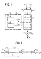
- Figure 1 shows the block formation diagram according to the prior art.
- the digital samples of the signals s 1 , ... s i , ... s N supplied by the N sensors are sequentially multiplexed in a multiplexer 10, controlled by a clock H, and are stored in a random access random access memory 11, RAM type.
- An address generator 12 supplies the write addresses A E and the read addresses A L to this memory 11.
- This memory works alternately in write mode and in read mode.
- the write mode corresponds to the acquisition of the N samples at the output of the multiplexer 10.
- the read mode is used for the calculation of the channels, which are obtained at the output of an adder 13, receiving the samples read in the memory 11 at the addresses where the samples with the delays necessary for the path to be formed are stored.
- FIG. 2 represents the writing-reading sequencing at the memory level.
- the period T s represents the sampling period of each sensor signal.
- the memory is managed so that between two periods T s the writing address A E is incremented by N, the samples being arranged successively from this address.
- the memory 11 is thus filled with a succession of P o groups G 1 , ... G Po of N samples separated by a time T s .
- ⁇ max be the greatest value of the delays ⁇ ik.
- a ⁇ T s ⁇ max ⁇ This value A ⁇ T s will be designated below by antenna depth.
- P o must be greater than or equal to A.
- the write addresses A E for the P groups of N samples are supplied by a counter 120, receiving the clock signals H.
- a signal sample from channel “k is formed by reading a sample from each sensor“ i ”in the groups corresponding to the delays ⁇ ik .
- the address generator 121 supplies the memory 11 with the reading addresses A L of the M samples necessary to form a channel sample because generally only part of the N sensors of the antenna are used to form each channel. .
- the address generator 121 performs the addition of the write address, which is incremented by one at each sampling period T s of the input signal, with the quantized delays ⁇ ik read from a memory read-only random access, type PROM.
- This delay memory also provides the index i of the sensor to be used at each step of the calculation and possibly the amplitude weighting A ik to be applied to the signals s 1 , ... s N of the sensors before summation, according to the relation (1 ).
- T v 1 / 2B, B being the necessary bandwidth.
- the sampling period T s is determined by the precision necessary for the delays and we generally have T s ⁇ T v .
- each memory storing samples of identical sensors over a period equal, as previously, to the antenna depth.
- the different calculation circuits can be controlled by the same address generator. However if the preformed tracks must be stabilized, by correcting the movements of the antenna, in roll and pitch for example, the circular symmetry disappears.
- address generators such as 12, as there are training circuits, a training circuit being defined as the memory 11 and summing assembly 13.
- an address generator has 2 to 3 times more components than a training circuit, which leads to large volumes of equipment.
- the digital channel-forming device makes it possible to reduce the material volume even in the case of antennas of any shape and to stabilize the channels in the event of movement of the platform supporting the antenna.
- a particular arrangement of the memory boxes and the storage of a time slot of the signal greater than the antenna depth makes it possible to obtain simultaneously several time samples of the same space channel during the same addressing of these memories.
- the address generator is unique, therefore much simpler than that which is necessary to simultaneously form several space channels according to the prior art.
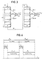
- two memories 30 and 31 are shown in series and each associated with an adder, respectively 32 and 33.
- P be the number of groups of N samples (it is determined by the size of the chosen memory module) contained in each of these memories.
- the time slot corresponding to each memory is therefore PT S. It is considered that the samples stored in these two memories correspond to two successive time slots: therefore at the same address the two memories contain samples of the same antenna sensor of index i but whose ages differ from PT S , which is achievable for example by supplying “in series” the memory 31 by the output W of the memory 30.
- the samples contained in the memory 30 are more recent than those contained in the memory 31 of the duration PT s .
- a sample of the direction track k relating to an instant t is formed by the addition of M samples 35.1, ... 35. (... 35.M taken successively from memory 30 at addresses depending on the index i of each sensor, on the index k of the channel and also on t / T s .
- the same addresses applied to memory 31 allow the calculation of a sample of channel from the same direction k but at the instant t-PT s , by taking the samples 36.1, ... 36.e, ... 36.M.
- T v being a multiple of T s and a submultiple of PT S.
- the ratio T v / T s is an integer generally between 2 and 8.
- each weighting and addition circuit must in reality have access to at least 2 adjacent memories which leads to the need to place memory selector circuits and to have at least Q + 1 memories available.
- the memory selector circuits are controlled synchronously by the address generator. If the antenna depth is greater than PT S each summing circuit must have access to more than 2 memories.
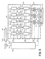
- FIG. 5 An example of the channel forming device according to the invention is shown in FIG. 5.
- It comprises an address generator 500, two random access memories, of RAM type, 510 and 520, called respectively acquisition memory and training memory and a summation assembly 530.
- the two memories 510 and 520 and the summation assembly 530 are arranged to constitute a number of forming circuits, equal to the number of operators 53.1, 53.2 and 53.3 of the assembly 530.
- An operator is the circuit which performs the operations ⁇ i A i ks i according to the relation (1).
- Q 3.
- each block 51.m of the acquisition memory is connected to the input of the corresponding block 52.m of the training memory.
- the acquisition memory 510 are written the samples of the sensors supplied by the multiplexer 10.
- the training memory 520 are read the samples of the sensors, and the outputs of the blocks of this memory are connected to the summation assembly 530.
- the generator of addresses 500 is common to the two memories 510 and 520 to which it provides the addressing and the write-read control signals.
- the age of the samples increases from left to right: the first block receives in series the samples from the sensors and the samples are transferred from one block to the adjacent block immediately to the right.
- These transfers are carried out in elementary read-write cycles sample by sample: during the read cycle, a sample is read from the memory blocks 51.1 ... 51.B and a sample is simultaneously stored in buffer registers 54.1 ... 54.B per block; during the writing cycle a sample is written in each block 51.1, ... 51.B.
- the addressing common to all the blocks is carried out by incrementing by 1 (modulo P x N) after each write.
- the number B of memories which is greater than the number Q of formative circuits is given by:
- the summing assembly 530 comprises Q selector circuits 56.1 ... 56.Q with several inputs and one output.
- the number of inputs corresponds to the number of adjacent memory blocks which is equal to 1 + whole part (A / P).
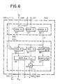
- the address generator is schematically represented in FIG. 6, it comprises two chains, the first chain 600 generating the addresses of the acquisition memory blocks whose write and read frequency is equal to N / T s while the second chain 610 delivers the addresses of the channel formation memory blocks.
- the first chain comprises a counter 60 modulo N which receives at 505 the clock signal at the frequency N / T s and which delivers to the output 506 a signal of period T s , for the multiplexer 10 (FIG. 5).
- the write addresses in the acquisition memory 510 are supplied to the output 501 by the counter 60 modulo N and a counter 61 modulo P, the counter 61 receiving the output signals from the counter 60.
- the output signal from the modulo counter P is applied to a modulo Q counter 62, which delivers the signal 1 for initialization of the second chain 610 to the output.
- the second chain for generating addresses comprises a counter 63 modulo M which receives at 505 the clock signals at period t o .
- a counter 64 modulo D where D is the number of channels to be formed, receives the output signals from counter 63.
- the two counters 63 and 64 supply the addresses applied to a read only memory 66 containing the electrical delay table Tik , the indices "I" of the sensors to be used and the amplitude weighting A ik to be applied to the signals according to the relation (1).
- a third counter 65 modulo PTs / T v fed by the counter 64 provides an offset, which is added at 68 to ⁇ ik to obtain the true delay.
- the offset increases by the quantity Tifs supplied by the memory 67 at each pulse of the counter 64.
- the read only memory 67 is supplied by the output of the counter 65.
- the most significant bits delivered by the adder 68 corresponding to an overflow of the capacity of the training memory block are used to control the memory block selectors at 503.
- the addresses are given, on the one hand at output 503 for rough addressing to selectors 56.1, ... 56.Q and on the other hand at 502 for fine modulo NP addressing to training memories 52.1, ... 52. Q.
- the output 504 provides the amplitude weights and a reset signal I k controlled by the counter 63 of modulo M.
- the acquisition memory 510 permanently acquires the samples of the sensors at the rate T s / N.
- the acquisition memory stores a time slot T of the signal from each sensor equal to BPT S , the value of which is greater than the antenna depth AT s .
- the device operates in cycles of duration T c , the duration of which corresponds to the time which is necessary to renew the samples of sensors.
- the two acquisition and training memories operate on cycles of duration T c .
- a cycle begins with the transfer of the content of the memory blocks 51.1 ... 51.B into the memory blocks 52.1 ... 52.B and this block by block, the blocks 51.m receiving the same addresses as the blocks 52 .m.
- the training memory 520 receives the addresses of the first chain of the address generator 500.
- the memory 520 is used in read-only mode for the formation of the channels during the training phase F.
- the duration of this phase F is T F.
- the transfer L j-1 of the samples of sensors E j-1 is carried out , followed by the formation of the samples of channels F j-1 .
- the transfer L j of the sensor samples E is carried out, followed by the formation of the channel samples F J.
- the operating frequencies of the two chains 600 and 610 of the address generator may be different, the second chain receiving the initialization order 1 at the end of the transfer.
- the channel formation circuit is specified to form a determined number D of space channels V k (t) sampled at period T v , each channel being formed from M sensors. Knowing that memory access time components or elementary cycle t o are used , the number Q of training circuits to be used is deduced therefrom to simultaneously obtain Q time samples from the same spatial channel.
- the device provides Q samples of the same space channel shifted in time by PT s , ie V k (t), V k (t-PT s ) ... V k (tT c ).
- PT s / T v channel samples by counting the intermediate samples.
- the calculation of a lane sample has a duration equal to Mt o .
- the calculation time for PT s / T v , channel samples for D channels is therefore equal to PT S / T v DMt o .
- the equality of the duration T F and of this calculation duration provides the number Q of forming circuits, namely:
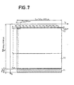
- FIGS. 7 and 8 represent, horizontally, the instants counted in periods T s in vertical function, instants counted in elementary cycles to for the channel samples calculated during each cycle T c .
- Part 70 corresponds to the calculation phase and part 71 to the transfer phase.
- FIG. 8 is a detail of the vertical scale of the part 72 of FIG. 7, that, for example, of the calculation cycle of all the samples of the space channel V I.
- the order of calculation of the channel samples can be modified. For example, after having calculated the first 13 samples of channel V, in FIG. 8, the first 13 samples of channel V 2 are then calculated, and so on until channel V 128 . The second line of the channel V 1 is then calculated, then the second line of the channel V 2 , etc. Other variants combining these two calculation orders are also possible.
- the directions of the D space channels are fixed relative to the antenna. It is possible to form paths in variable directions over time, either to compensate for the movements of the platform supporting the antenna, or to track mobile sources.
- the read only memory 66 containing the addresses of the sensors i and T ik must be replaced by a random access memory refreshed periodically by a computer, receiving the position parameters of this mobile platform.
- a track V k being defined for example by absolute spherical coordinates and the angles of rotation of the boat being measured
- a computer determines the spherical coordinates of the tracks relating to the boat. From these values knowing the geometry from the antenna, the computer determines the Tik values which are stored in the RAM.
- This renewal period must be equal to or multiple of the duration of the cycle T c during which the channel forming circuits simultaneously calculate several time samples of the same channel.
- the duration of the cycle T c is of the order of 13 milliseconds, which would make it possible to maintain a pointing accuracy to the nearest 0.1 degrees up to angular speeds of 7.5 degrees per second.
- the device according to the invention is particularly advantageous for the formation of the standby channels of a sonar using a conforming antenna, that is to say which matches the shape of the section of the ship or submarine.
- the number of boxes would have been of the order of 250 boxes, making best use of the left-right symmetry which generally exists in a conforming antenna.
Landscapes
- Engineering & Computer Science (AREA)
- Physics & Mathematics (AREA)
- Radar, Positioning & Navigation (AREA)
- Remote Sensing (AREA)
- Acoustics & Sound (AREA)
- Computer Networks & Wireless Communication (AREA)
- General Physics & Mathematics (AREA)
- Multimedia (AREA)
- Radar Systems Or Details Thereof (AREA)
- Measurement Of Velocity Or Position Using Acoustic Or Ultrasonic Waves (AREA)
Claims (4)
dadurch gekennzeichnet, daß
Applications Claiming Priority (2)
| Application Number | Priority Date | Filing Date | Title |
|---|---|---|---|
| FR8217742A FR2535067A1 (fr) | 1982-10-22 | 1982-10-22 | Dispositif numerique de formation de voies sonar |
| FR8217742 | 1982-10-22 |
Publications (2)
| Publication Number | Publication Date |
|---|---|
| EP0109869A1 EP0109869A1 (de) | 1984-05-30 |
| EP0109869B1 true EP0109869B1 (de) | 1988-03-02 |
Family
ID=9278521
Family Applications (1)
| Application Number | Title | Priority Date | Filing Date |
|---|---|---|---|
| EP83401973A Expired EP0109869B1 (de) | 1982-10-22 | 1983-10-10 | Digitales Sonarstrahlbündelungsgerät |
Country Status (4)
| Country | Link |
|---|---|
| US (1) | US4604736A (de) |
| EP (1) | EP0109869B1 (de) |
| DE (1) | DE3375836D1 (de) |
| FR (1) | FR2535067A1 (de) |
Families Citing this family (9)
| Publication number | Priority date | Publication date | Assignee | Title |
|---|---|---|---|---|
| FR2652164A1 (fr) * | 1989-09-15 | 1991-03-22 | Thomson Csf | Procede de formation de voies pour sonar, notamment pour sonar remorque. |
| US5185874A (en) * | 1989-10-30 | 1993-02-09 | Tektronix, Inc. | Address generator for high speed data averager |
| EP0472736A1 (de) * | 1990-03-09 | 1992-03-04 | Fujitsu Limited | Abgetasteter datenspeicher und aufbereitungssystem |
| GB9014544D0 (en) * | 1990-06-29 | 1990-08-22 | Univ Heriot Watt | Methods and apparatus for acoustic holographic imaging in marine and other acoustic remote sensing equipment |
| US5469851A (en) * | 1994-08-09 | 1995-11-28 | Hewlett-Packard Company | Time multiplexed digital ultrasound beamformer |
| FR2732787B1 (fr) * | 1995-04-07 | 1997-05-16 | Thomson Csf | Procede de saisie graphique d'application de traitement de signal |
| FR2748138B1 (fr) * | 1996-04-26 | 1998-07-10 | Thomson Csf | Procede de codage pour processeur de traitement de signal, et processeur pour la mise en oeuvre d'un tel procede |
| FR2785406B1 (fr) | 1998-10-30 | 2004-09-10 | Thomson Marconi Sonar Sas | Memoire a acces vectoriel |
| EP2929437B1 (de) * | 2012-12-07 | 2017-09-20 | Sonelite Inc. | Direktes daten-an-speicher-system und zugehörige betriebsverfahren |
Family Cites Families (7)
| Publication number | Priority date | Publication date | Assignee | Title |
|---|---|---|---|---|
| US4001763A (en) * | 1975-02-03 | 1977-01-04 | Raytheon Company | Electronically stabilized beam former system |
| US4074223A (en) * | 1976-08-03 | 1978-02-14 | Indianapolis Center For Advanced Research | Peak detector for resolution enhancement of ultrasonic visualization systems |
| US4267584A (en) * | 1977-07-01 | 1981-05-12 | Siemens Gammasonics, Inc. | Permutating analog shift register variable delay system |
| US4170766A (en) * | 1978-01-27 | 1979-10-09 | Raytheon Company | Beamformer |
| FR2472753A1 (fr) * | 1979-12-31 | 1981-07-03 | Anvar | Perfectionnements aux dispositifs de sondage par ultra-sons |
| US4325257A (en) * | 1980-02-20 | 1982-04-20 | Kino Gordon S | Real-time digital, synthetic-focus, acoustic imaging system |
| US4336607A (en) * | 1980-12-10 | 1982-06-22 | The United States Of America As Represented By The Secretary Of The Navy | Beamformer having random access memory delay |
-
1982
- 1982-10-22 FR FR8217742A patent/FR2535067A1/fr active Granted
-
1983
- 1983-10-10 DE DE8383401973T patent/DE3375836D1/de not_active Expired
- 1983-10-10 EP EP83401973A patent/EP0109869B1/de not_active Expired
- 1983-10-21 US US06/544,412 patent/US4604736A/en not_active Expired - Fee Related
Also Published As
| Publication number | Publication date |
|---|---|
| FR2535067B1 (de) | 1985-01-18 |
| EP0109869A1 (de) | 1984-05-30 |
| US4604736A (en) | 1986-08-05 |
| FR2535067A1 (fr) | 1984-04-27 |
| DE3375836D1 (en) | 1988-04-07 |
Similar Documents
| Publication | Publication Date | Title |
|---|---|---|
| EP0050060B1 (de) | Bilderzeugungssystem mit gleichzeitiger mehrfacher Aussendung | |
| CA1124826A (en) | Beamformer | |
| US4403314A (en) | Active detection system using simultaneous multiple transmissions | |
| US4207620A (en) | Oceanographic mapping system | |
| Blackinton et al. | First results from a combination side-scan sonar and seafloor mapping system (SeaMARC II) | |
| EP0109869B1 (de) | Digitales Sonarstrahlbündelungsgerät | |
| US3484737A (en) | Acoustic mapping apparatus | |
| FR2552905A1 (fr) | Radar fonctionnant en ondes entretenues capable d'effectuer des mesures de distance | |
| FR2461265A1 (fr) | Dispositif de formation d'image par ultrasons a commande numerique, notamment pour le diagnostic medical | |
| FR2478824A1 (fr) | Systeme d'imagerie acoustique | |
| Roux et al. | A nonreciprocal implementation of time reversal in the ocean | |
| CA1101981A (en) | Beam forming system | |
| US3449711A (en) | Beam former | |
| FR2528185A1 (fr) | Procede de localisation sous-marine au moyen d'impulsions sonores et dispositif pour sa mise en oeuvre | |
| EP0093057A1 (de) | Adaptive Filtereinrichtung für die von einem aktiven Sonar empfangenen Signale zur Nachhallunterdrückung | |
| US5638821A (en) | Ultrasound diagnostics system for obtaining a tomographic image | |
| FR2501870A1 (fr) | Procede et appareil de diagraphie pour un sondage | |
| US4471473A (en) | Direction finding circuit arrangement | |
| FR2545612A1 (fr) | Simulateur d'effet doppler a large bande | |
| FR2459486A1 (fr) | Procede d'affichage de signaux de localisation par reflexion d'onde et dispositif pour sa mise en oeuvre, notamment pour radar ou sonar | |
| Spiess | Acoustic imaging | |
| JPH04104079A (ja) | ソナー立体表示装置 | |
| Pitt et al. | Design and implementation of a digital phase shift beamformer | |
| Naik et al. | Evolution of Sonar Survey Systems for Sea Floor Studies | |
| FR2697346A1 (fr) | Dispositif de sondage ultrasonore à commande numérique de phase. |
Legal Events
| Date | Code | Title | Description |
|---|---|---|---|
| PUAI | Public reference made under article 153(3) epc to a published international application that has entered the european phase |
Free format text: ORIGINAL CODE: 0009012 |
|
| AK | Designated contracting states |
Designated state(s): DE GB NL |
|
| 17P | Request for examination filed |
Effective date: 19841005 |
|
| 17Q | First examination report despatched |
Effective date: 19860428 |
|
| R17C | First examination report despatched (corrected) |
Effective date: 19860708 |
|
| GRAA | (expected) grant |
Free format text: ORIGINAL CODE: 0009210 |
|
| AK | Designated contracting states |
Kind code of ref document: B1 Designated state(s): DE GB NL |
|
| REF | Corresponds to: |
Ref document number: 3375836 Country of ref document: DE Date of ref document: 19880407 |
|
| GBT | Gb: translation of ep patent filed (gb section 77(6)(a)/1977) | ||
| PLBI | Opposition filed |
Free format text: ORIGINAL CODE: 0009260 |
|
| 26 | Opposition filed |
Opponent name: KRUPP ATLAS ELEKTRONIK GMBH Effective date: 19881102 |
|
| NLR1 | Nl: opposition has been filed with the epo |
Opponent name: KRUPP ATLAS ELEKTRONIK GMBH |
|
| RAP4 | Party data changed (patent owner data changed or rights of a patent transferred) |
Owner name: THOMSON-CSF |
|
| PGFP | Annual fee paid to national office [announced via postgrant information from national office to epo] |
Ref country code: NL Payment date: 19901031 Year of fee payment: 8 |
|
| PGFP | Annual fee paid to national office [announced via postgrant information from national office to epo] |
Ref country code: GB Payment date: 19910920 Year of fee payment: 9 |
|
| PGFP | Annual fee paid to national office [announced via postgrant information from national office to epo] |
Ref country code: DE Payment date: 19910924 Year of fee payment: 9 |
|
| PG25 | Lapsed in a contracting state [announced via postgrant information from national office to epo] |
Ref country code: NL Effective date: 19920501 |
|
| NLV4 | Nl: lapsed or anulled due to non-payment of the annual fee | ||
| PG25 | Lapsed in a contracting state [announced via postgrant information from national office to epo] |
Ref country code: GB Effective date: 19921010 |
|
| RDAG | Patent revoked |
Free format text: ORIGINAL CODE: 0009271 |
|
| STAA | Information on the status of an ep patent application or granted ep patent |
Free format text: STATUS: PATENT REVOKED |
|
| GBPC | Gb: european patent ceased through non-payment of renewal fee |
Effective date: 19921010 |
|
| 27W | Patent revoked |
Effective date: 19930308 |