EP0108945B1 - Hochspannungshalbleiteranordnungen mit reduziertem Leitungswiderstand - Google Patents
Hochspannungshalbleiteranordnungen mit reduziertem Leitungswiderstand Download PDFInfo
- Publication number
- EP0108945B1 EP0108945B1 EP83110354A EP83110354A EP0108945B1 EP 0108945 B1 EP0108945 B1 EP 0108945B1 EP 83110354 A EP83110354 A EP 83110354A EP 83110354 A EP83110354 A EP 83110354A EP 0108945 B1 EP0108945 B1 EP 0108945B1
- Authority
- EP
- European Patent Office
- Prior art keywords
- region
- semiconductor device
- layer
- bulk substrate
- switching means
- Prior art date
- Legal status (The legal status is an assumption and is not a legal conclusion. Google has not performed a legal analysis and makes no representation as to the accuracy of the status listed.)
- Expired
Links
Images
Classifications
-
- H—ELECTRICITY
- H10—SEMICONDUCTOR DEVICES; ELECTRIC SOLID-STATE DEVICES NOT OTHERWISE PROVIDED FOR
- H10D—INORGANIC ELECTRIC SEMICONDUCTOR DEVICES
- H10D62/00—Semiconductor bodies, or regions thereof, of devices having potential barriers
- H10D62/10—Shapes, relative sizes or dispositions of the regions of the semiconductor bodies; Shapes of the semiconductor bodies
- H10D62/17—Semiconductor regions connected to electrodes not carrying current to be rectified, amplified or switched, e.g. channel regions
- H10D62/177—Base regions of bipolar transistors, e.g. BJTs or IGBTs
-
- H—ELECTRICITY
- H10—SEMICONDUCTOR DEVICES; ELECTRIC SOLID-STATE DEVICES NOT OTHERWISE PROVIDED FOR
- H10D—INORGANIC ELECTRIC SEMICONDUCTOR DEVICES
- H10D8/00—Diodes
- H10D8/50—PIN diodes
-
- H—ELECTRICITY
- H10—SEMICONDUCTOR DEVICES; ELECTRIC SOLID-STATE DEVICES NOT OTHERWISE PROVIDED FOR
- H10D—INORGANIC ELECTRIC SEMICONDUCTOR DEVICES
- H10D84/00—Integrated devices formed in or on semiconductor substrates that comprise only semiconducting layers, e.g. on Si wafers or on GaAs-on-Si wafers
- H10D84/60—Integrated devices formed in or on semiconductor substrates that comprise only semiconducting layers, e.g. on Si wafers or on GaAs-on-Si wafers characterised by the integration of at least one component covered by groups H10D10/00 or H10D18/00, e.g. integration of BJTs
- H10D84/611—Combinations of BJTs and one or more of diodes, resistors or capacitors
- H10D84/613—Combinations of vertical BJTs and one or more of diodes, resistors or capacitors
- H10D84/617—Combinations of vertical BJTs and only diodes
-
- H—ELECTRICITY
- H10—SEMICONDUCTOR DEVICES; ELECTRIC SOLID-STATE DEVICES NOT OTHERWISE PROVIDED FOR
- H10D—INORGANIC ELECTRIC SEMICONDUCTOR DEVICES
- H10D84/00—Integrated devices formed in or on semiconductor substrates that comprise only semiconducting layers, e.g. on Si wafers or on GaAs-on-Si wafers
- H10D84/80—Integrated devices formed in or on semiconductor substrates that comprise only semiconducting layers, e.g. on Si wafers or on GaAs-on-Si wafers characterised by the integration of at least one component covered by groups H10D12/00 or H10D30/00, e.g. integration of IGFETs
- H10D84/811—Combinations of field-effect devices and one or more diodes, capacitors or resistors
-
- H—ELECTRICITY
- H10—SEMICONDUCTOR DEVICES; ELECTRIC SOLID-STATE DEVICES NOT OTHERWISE PROVIDED FOR
- H10W—GENERIC PACKAGES, INTERCONNECTIONS, CONNECTORS OR OTHER CONSTRUCTIONAL DETAILS OF DEVICES COVERED BY CLASS H10
- H10W10/00—Isolation regions in semiconductor bodies between components of integrated devices
- H10W10/01—Manufacture or treatment
- H10W10/031—Manufacture or treatment of isolation regions comprising PN junctions
-
- H—ELECTRICITY
- H10—SEMICONDUCTOR DEVICES; ELECTRIC SOLID-STATE DEVICES NOT OTHERWISE PROVIDED FOR
- H10W—GENERIC PACKAGES, INTERCONNECTIONS, CONNECTORS OR OTHER CONSTRUCTIONAL DETAILS OF DEVICES COVERED BY CLASS H10
- H10W10/00—Isolation regions in semiconductor bodies between components of integrated devices
- H10W10/30—Isolation regions comprising PN junctions
Definitions
- the present invention relates to a high voltage semiconductor device according to the prior-art portion of claim 1.
- a high voltage semiconductor device of this type is described in DE ⁇ A ⁇ 2 102 103.
- This known semiconductor device comprises a bulk substrate of one conductivity type with a layer of opposite conductivity type thereon. There are furthermore provided three regions extending into the layer from the upper surface thereof, wherein the first region is of the opposite conductivity type and the second and third regions are of the one conductivity type. The first and second regions therefore are forming the cathode and the anode, respectively, of a diode.
- the third region is interposed between the cathode and anode regions and as it form a P-N junction with the layer it can be used as a gate, so that during the forward bias condition of the diode the degree of conductivity of the layer between the cathode and anode regions can be controlled by suitably biasing the gate.
- the diode when the gate is biased to be more negative than the threshold voltage the diode is in a current-blocking state, whereas the on-resistance of the diode is more and more reduced when the gate is gradually made less negative than the threshold voltage.
- the value of on-resistance of this known semiconductor device cannot be made smaller than the value of on-resistance of a conventional diode having no gate.
- This device comprises a thin N- layer atop a P- substrate, wherein a N + cathode region and a P + anode region are extending into the N- layer from its upper surface, the anode region surrounding the cathode region.
- an N + buried layer exists between the P- substrate and the N- layer, beneath the P + anode region, so as to surround the N + cathode region.
- a further P + region extends into the N - layer from its upper surface and is interposed between the cathode region and the anode region so as to surround the cathode region and, in turn, be surrounded by the anode region.
- the further P + region is permanently biased near or at the potential of the substrate, whereby the N- layer supports reverse voltages in the device.
- P-N diode attains a reasonably low value of on-resistance. It would be desirable, however, to provide a diode having an even lower value of on-resistance. It furthermore would be desirable to provide the same low value of on-resistance for a semiconductor device forming a bipolar transistor.
- the invention there can be obtained a semiconductor device whose on-resistance is dramatically reduced, so that power losses and voltage drop across the .device are correspondingly reduced. Furthermore the device can easily be formed as a P-N diode or as a bipolar transistor. Finally it is possible to form semiconductor devices employed to attain such reduced on-resistance along with such a high voltage semiconductor device in a single integrated circuit.
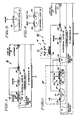
- FIG. 1 illustrates a portion of a P-N diode 10 to the left of a line of symmetry 12.
- P-N diode 10 suitably comprises a bulk P- substrate 14, preferably silicon, with an N- layer 16 thereon, preferably an epitaxial silicon layer.
- An N + cathode region 18 extends into the N- layer 16 from the upper surface thereof.
- a P + anode region 20 extends into N- layer 16 from its upper surface and surrounds N + region 18 as viewed from above.
- N + buried layer 22 is situated between N-layer 16 and P- substrate 14, beneath P + anode region 20 and surrounds N + cathode region 18.
- a further P + region 24 extends into N- layer 16 from its upper surface, surrounds N + cathode region 18, and, in turn, is surrounded by P + anode region 20.
- a P + isolation region 26 is integrally connected to P- substrate 14, and surrounds the periphery of N- layer 16, thereby enabling other semiconductor devices to be formed, along with P-N diode 10, in an integrated circuit.
- N + buried layer 22 in P ⁇ N . diode 10 serves to reduce parasitic currents in diode 10 that otherwise would exist.
- P + region 24 appropriately biased to a potential approximately equal to or slightly more positive than that of P- substrate 14 when diode 10 is in a current-blocking state, enables the portion of N- epitaxial layer 16 between P + region 24 and N + cathode 18 to support high reverse voltages. This is because, without P + region 24 so biased N + buried layer 22 would rise in potential to that of N + cathode 18, leaving only the thin region of N-layer 16 between N + buried layer 22 and P + anode region 20 to support reverse voltages. Such thin region of N- layer 16 would likely break down under high reverse voltage.
- bias means 28 for supplying P + region 24 with a plurality of different bias drives so as to differently bias P-N junction 32, extant between P + region 24 and N-layer 16.
- the different biasing conditions of P-N junction 32 serve to effect different degrees of conductivity in the N- layer 16 between P + anode region 20 and N + cathode region 18, as will be described more fully hereinbelow.
- Bias means 28 in the exemplary embodiment illustrated, comprises a depletion mode (i.e., normally-conducting) P-channel metal-oxide- semiconductor field effect transistor (MOSFET) 34.
- MOSFET 34 in the absence of any bias voltage on its gate 36, electrically shorts P + region 24 to P + isolation region 26, which is at the potential of P- substrate 14. This is because, in such state of MOSFET 34, P-channel 38 of MOSFET 34 provides a high conductivity path between p + region 40, which is electrically shorted to P + region 24, and p + isolation region 26.
- P + region 24 When gate 36 is biased with a positive voltage in excess of a threshold value so as to deplete P-channel 38 of holes and thereby reduce it conductivity, P + region 24 is open circuited, that is, supplied with a bias drive of zero current.
- This zero current bias drive of P + region 24 advantageously results in P-N diode 10 having a lower value of on-resistance than if P + region 24 were biased to the potential of P-substrate 14. This is because, in P-N diode 10, there is a much smaller depletion region extending into N- layer 16 from P-N junction 32, in contrast to the case where P + region 24 is biased to the P- substrate.14 potential, such as appertains to the P-N diode of the above-referenced application.
- Bias means 28 with MOSFET 34 is preferably formed along with P-N diode 10 in a single integrated circuit.
- bias means 28 could be implemented as a separate device.
- Bias means 28 is an exemplary bias means for P + region 24, and could be implemented in many different forms.
- MOSFET 34 of bias means 28 could be replaced by other switching means, such as a bipolar transistor.
- the bias means for P + region 24 could be implemented as a bias means 28', which is illustrated in Figure 2.
- FIG. 2 depicts a P-N diode 40, which is identical to P-N diode 10 ( Figure 1) except for the inclusion of a different bias means 28' for the corresponding P + region 24', shown to the left of P + isolation region 26'.
- the different bias means 28' includes a resistance means 50 of ohmic value R having a terminal 52 adapted to be connected to a source of voltage (not shown) so as to be biased at a positive voltage, V s , and a further terminal 54, which is connected to P + region 24'.
- Bias means 28' further includes an enhancement mode or normally-off MOSFET 56.
- One terminal 58 of MOSFET 56 is electrically shorted, via electrode 60, to P + isolation region 26', which is at the potential of P- substrate 14.
- Another terminal 62 of MOSFET 56 is electrically shorted, via conductor 68, to P + region 24'.
- Bias means 28' is effective to produce, via conductor 68, two different bias drives on P + region 24'. These two different bias drives can be readily understood by considering voltage pulses 70 and 72, which can be determined by monitoring gate 74 of MOSFET 56 and conductor 68, respectively.
- the voltage on conductor 68 is equal to the bias voltage V s on terminal 52, reduced by the IR (or currentx resistance) voltage drop across resistance means 50. Consequently, P + region 24' is supplied with a bias drive characterized by the voltage on conductor 68 and by a current limited by the combined resistances of the voltage source (not shown) which biases terminal 52 to V s volts, the resistance means 50, and the resistance through P + region 24' to a ground or reference level.
- an inversion layer is formed in region 76 of MOSFET 56, beneath gate 74.
- the inversion layer is highly conductive to electrons, and, together with N + regions 78 and 80, completes a current path from terminal 58, which is at the potential of P-substrate 14', to conductor 68, via terminal 62, thereby biasing conductor 68 to the potential of P- substrate 14'.
- conductor 68 so biased P + region 24' is supplied with a bias drive characterized by the P- substrate 14' potential and by no current (or zero level current), since P-N junction 32', between P + region 24' and N- layer 16' is reverse biased.
- P + region 24' When P-N diode 40 is operating in its current-blocking state, P + region 24' should be supplied with a bias drive characterized by the potential of P- substrate 14' and zero current. When P-N diode 40 is operating in its current-conducting state, however, P + region 24' should be supplied with a bias drive characterized by being at the potential V s , as reduced by the IR voltage drop across resistance means 50.
- P-N junction 32' between P + region 24' and N- layer 16', is forward biased, and, in accordance with an important aspect of the present invention P + region 24' thereby injects holes into N- layer 16'. Then, in accordance with the principle of quasi-neutrality (as discussed for example, in R. S. Muller and T. I.
- resistance means 50 and MOSFET 56 are illustrated in the preferred embodiment in which they are formed along with P-N diode 40 in a single integrated circuit, such devices could alternatively be formed as separate devices. If devices 50 and 56 are formed in a single integrated circuit as illustrated, it is desirable that P + isolation region 26' be interposed between P-N diode 40 and such devices. P + isolation region 26' could be omitted, however, if the distance of separation between P-N diode 40 and such devices is sufficient to prevent adverse electrical interference therebetween, although this would result in more space consumed in the integrated circuit.
- the present invention is also useful in semiconductor devices other than P-N diodes, such as bipolar transistors.
- To make a bipolar transistor requires a variation of the structure associated with P * anode region 20 ( Figure 1), which is illustrated in the detail view of Figure 3.
- Appropriate modified structure is shown i Figure 4, in which P base region 120 corresponds to P* anode region 20 of Figure 3.
- N + emitter region 190 extends into P base region 120 from the upper surface of region 120, and surrounds an N + collector region (not illustrated) which corresponds to N + cathode region 18 of P-N diode 10 ( Figure 1).
- each of the regions shown as extending into a device from the upper surface thereof can be formed by either diffusion or ion implantation, and the N + buried layers can be formed by either diffusion or ion implantation through the upper surface of the respective P- substrate prior to the growth of the respective N- epitaxial layer thereon.
- the mathematical product of the thickness and doping concentration of the N- epitaxial layer of each device described herein is selected in accordance with Reduced Surface Field (or RESURF) Technology in order to maximize the reverse voltage attainable by each device.
- RESURF Reduced Surface Field
- Details of RESURF Technology may be found, for example, in an article by J. A. Appels and H. M. J. Vaes "High Voltage Thin Layer Devices (RESURF Devices)", Proceedings of the 1979 IEEE International Electron Device Meeting, pages 238-241, as well as in an article by S. Colak, B. Singer and E. Stupp. "Design of High-Density Power Lateral DMOS Transistors", Proceedings of the 1980 IEEE Power Electronics Specialists Conference, pages 164-167.
Landscapes
- Metal-Oxide And Bipolar Metal-Oxide Semiconductor Integrated Circuits (AREA)
- Semiconductor Integrated Circuits (AREA)
Claims (19)
Applications Claiming Priority (2)
| Application Number | Priority Date | Filing Date | Title |
|---|---|---|---|
| US43624482A | 1982-10-25 | 1982-10-25 | |
| US436244 | 1982-10-25 |
Publications (2)
| Publication Number | Publication Date |
|---|---|
| EP0108945A1 EP0108945A1 (de) | 1984-05-23 |
| EP0108945B1 true EP0108945B1 (de) | 1987-03-11 |
Family
ID=23731686
Family Applications (1)
| Application Number | Title | Priority Date | Filing Date |
|---|---|---|---|
| EP83110354A Expired EP0108945B1 (de) | 1982-10-25 | 1983-10-18 | Hochspannungshalbleiteranordnungen mit reduziertem Leitungswiderstand |
Country Status (3)
| Country | Link |
|---|---|
| EP (1) | EP0108945B1 (de) |
| JP (1) | JPS5994453A (de) |
| DE (1) | DE3370250D1 (de) |
Families Citing this family (3)
| Publication number | Priority date | Publication date | Assignee | Title |
|---|---|---|---|---|
| DE4143209A1 (de) * | 1991-12-30 | 1993-07-01 | Hoefflinger Bernd Prof Dr | Integrierte schaltung |
| JP3400853B2 (ja) * | 1994-04-27 | 2003-04-28 | 三菱電機株式会社 | 半導体装置 |
| GB2409603B (en) * | 2003-12-23 | 2007-10-10 | Ipwireless Inc | Method and arrangement for power control in a radio communication system |
Family Cites Families (7)
| Publication number | Priority date | Publication date | Assignee | Title |
|---|---|---|---|---|
| DE2102103A1 (de) * | 1970-01-22 | 1971-07-29 | Rca Corp | Durch Feldeffekt gesteuerte Diode |
| DE2007627B2 (de) * | 1970-02-19 | 1973-03-22 | Licentia Patent-Verwaltungs-Gmbh, 6000 Frankfurt | Verfahren zum herstellen einer integrierten halbleiterschaltung |
| JPS5935183B2 (ja) * | 1975-08-20 | 1984-08-27 | サンケイ電気 (株) | シヨツトキバリア半導体装置 |
| GB1558506A (en) * | 1976-08-09 | 1980-01-03 | Mullard Ltd | Semiconductor devices having a rectifying metalto-semicondductor junction |
| GB1587540A (en) * | 1977-12-20 | 1981-04-08 | Philips Electronic Associated | Gate turn-off diodes and arrangements including such diodes |
| JPS562622A (en) * | 1979-06-22 | 1981-01-12 | Nichicon Capacitor Ltd | Method of sealing electrolytic condenser |
| US4494134A (en) * | 1982-07-01 | 1985-01-15 | General Electric Company | High voltage semiconductor devices comprising integral JFET |
-
1983
- 1983-10-12 JP JP58189393A patent/JPS5994453A/ja active Pending
- 1983-10-18 DE DE8383110354T patent/DE3370250D1/de not_active Expired
- 1983-10-18 EP EP83110354A patent/EP0108945B1/de not_active Expired
Also Published As
| Publication number | Publication date |
|---|---|
| EP0108945A1 (de) | 1984-05-23 |
| DE3370250D1 (en) | 1987-04-16 |
| JPS5994453A (ja) | 1984-05-31 |
Similar Documents
| Publication | Publication Date | Title |
|---|---|---|
| US4967243A (en) | Power transistor structure with high speed integral antiparallel Schottky diode | |
| US5702961A (en) | Methods of forming insulated gate bipolar transistors having built-in freewheeling diodes and transistors formed thereby | |
| US8629509B2 (en) | High voltage insulated gate bipolar transistors with minority carrier diverter | |
| US9941274B2 (en) | Semiconductor device with a switchable and a non-switchable diode region | |
| US4969028A (en) | Gate enhanced rectifier | |
| US4494134A (en) | High voltage semiconductor devices comprising integral JFET | |
| US4989058A (en) | Fast switching lateral insulated gate transistors | |
| US4060821A (en) | Field controlled thyristor with buried grid | |
| JPH0758784B2 (ja) | ラッチ・アップ防止性能を改良したラテラル形絶縁ゲート・バイポーラ・トランジスタ | |
| KR102246570B1 (ko) | 전력 반도체 장치 | |
| EP0522670B1 (de) | Schnellschaltender, lateraler Feldeffekttransistor mit isolierter Steuerelektrode | |
| US5910664A (en) | Emitter-switched transistor structures | |
| US5430323A (en) | Injection control-type Schottky barrier rectifier | |
| US5886384A (en) | Semiconductor component with linear current to voltage characteristics | |
| EP0338312B1 (de) | Bipolarer Transistor mit isolierter Steuerelektrode | |
| US4132996A (en) | Electric field-controlled semiconductor device | |
| SE513284C3 (sv) | Halvledarkomponent med linjär ström-till-spänningskarakteristik | |
| EP1022785B1 (de) | Elektronische Halbleiterleistungsanordnung mit integrierter Diode | |
| US4942440A (en) | High voltage semiconductor devices with reduced on-resistance | |
| EP0115098B1 (de) | Laterale DMOS-Transistoranordnung mit einer Injektionszone | |
| US4862242A (en) | Semiconductor wafer with an electrically-isolated semiconductor device | |
| US4868921A (en) | High voltage integrated circuit devices electrically isolated from an integrated circuit substrate | |
| US10600898B2 (en) | Vertical bidirectional insulated gate turn-off device | |
| EP0144865B1 (de) | Halbleitersubstrat mit einer elektrisch isolierten Halbleiteranordnung | |
| EP0108945A1 (de) | Hochspannungshalbleiteranordnungen mit reduziertem Leitungswiderstand |
Legal Events
| Date | Code | Title | Description |
|---|---|---|---|
| PUAI | Public reference made under article 153(3) epc to a published international application that has entered the european phase |
Free format text: ORIGINAL CODE: 0009012 |
|
| AK | Designated contracting states |
Designated state(s): CH DE FR GB LI NL SE |
|
| 17P | Request for examination filed |
Effective date: 19840603 |
|
| GRAA | (expected) grant |
Free format text: ORIGINAL CODE: 0009210 |
|
| AK | Designated contracting states |
Kind code of ref document: B1 Designated state(s): CH DE FR GB LI NL SE |
|
| REF | Corresponds to: |
Ref document number: 3370250 Country of ref document: DE Date of ref document: 19870416 |
|
| ET | Fr: translation filed | ||
| PLBE | No opposition filed within time limit |
Free format text: ORIGINAL CODE: 0009261 |
|
| STAA | Information on the status of an ep patent application or granted ep patent |
Free format text: STATUS: NO OPPOSITION FILED WITHIN TIME LIMIT |
|
| 26N | No opposition filed | ||
| PGFP | Annual fee paid to national office [announced via postgrant information from national office to epo] |
Ref country code: SE Payment date: 19890926 Year of fee payment: 7 |
|
| PGFP | Annual fee paid to national office [announced via postgrant information from national office to epo] |
Ref country code: CH Payment date: 19890927 Year of fee payment: 7 |
|
| PGFP | Annual fee paid to national office [announced via postgrant information from national office to epo] |
Ref country code: GB Payment date: 19890930 Year of fee payment: 7 |
|
| PGFP | Annual fee paid to national office [announced via postgrant information from national office to epo] |
Ref country code: FR Payment date: 19891004 Year of fee payment: 7 |
|
| PGFP | Annual fee paid to national office [announced via postgrant information from national office to epo] |
Ref country code: DE Payment date: 19891019 Year of fee payment: 7 |
|
| PGFP | Annual fee paid to national office [announced via postgrant information from national office to epo] |
Ref country code: NL Payment date: 19891031 Year of fee payment: 7 |
|
| PG25 | Lapsed in a contracting state [announced via postgrant information from national office to epo] |
Ref country code: GB Effective date: 19901018 |
|
| PG25 | Lapsed in a contracting state [announced via postgrant information from national office to epo] |
Ref country code: SE Effective date: 19901019 |
|
| PG25 | Lapsed in a contracting state [announced via postgrant information from national office to epo] |
Ref country code: LI Effective date: 19901031 Ref country code: CH Effective date: 19901031 |
|
| PG25 | Lapsed in a contracting state [announced via postgrant information from national office to epo] |
Ref country code: NL Effective date: 19910501 |
|
| GBPC | Gb: european patent ceased through non-payment of renewal fee | ||
| NLV4 | Nl: lapsed or anulled due to non-payment of the annual fee | ||
| PG25 | Lapsed in a contracting state [announced via postgrant information from national office to epo] |
Ref country code: FR Effective date: 19910628 |
|
| REG | Reference to a national code |
Ref country code: CH Ref legal event code: PL |
|
| PG25 | Lapsed in a contracting state [announced via postgrant information from national office to epo] |
Ref country code: DE Effective date: 19910702 |
|
| REG | Reference to a national code |
Ref country code: FR Ref legal event code: ST |
|
| EUG | Se: european patent has lapsed |
Ref document number: 83110354.4 Effective date: 19910603 |