EP0106752B1 - Verfahren zur Herstellung von Lichtwellenleitern - Google Patents
Verfahren zur Herstellung von Lichtwellenleitern Download PDFInfo
- Publication number
- EP0106752B1 EP0106752B1 EP83401927A EP83401927A EP0106752B1 EP 0106752 B1 EP0106752 B1 EP 0106752B1 EP 83401927 A EP83401927 A EP 83401927A EP 83401927 A EP83401927 A EP 83401927A EP 0106752 B1 EP0106752 B1 EP 0106752B1
- Authority
- EP
- European Patent Office
- Prior art keywords
- layer
- refractive index
- silica
- tube
- transformable
- Prior art date
- Legal status (The legal status is an assumption and is not a legal conclusion. Google has not performed a legal analysis and makes no representation as to the accuracy of the status listed.)
- Expired
Links
- 238000004519 manufacturing process Methods 0.000 title claims description 13
- VYPSYNLAJGMNEJ-UHFFFAOYSA-N Silicium dioxide Chemical compound O=[Si]=O VYPSYNLAJGMNEJ-UHFFFAOYSA-N 0.000 claims description 125
- 239000000377 silicon dioxide Substances 0.000 claims description 61
- 239000002019 doping agent Substances 0.000 claims description 40
- 150000001875 compounds Chemical class 0.000 claims description 32
- 239000000463 material Substances 0.000 claims description 26
- 235000012431 wafers Nutrition 0.000 claims description 22
- 235000012239 silicon dioxide Nutrition 0.000 claims description 17
- XUIMIQQOPSSXEZ-UHFFFAOYSA-N Silicon Chemical compound [Si] XUIMIQQOPSSXEZ-UHFFFAOYSA-N 0.000 claims description 15
- 230000001590 oxidative effect Effects 0.000 claims description 10
- 230000003287 optical effect Effects 0.000 claims description 9
- 229910052710 silicon Inorganic materials 0.000 claims description 9
- 239000010703 silicon Substances 0.000 claims description 9
- 238000000034 method Methods 0.000 claims description 7
- 238000010894 electron beam technology Methods 0.000 claims description 5
- 238000001704 evaporation Methods 0.000 claims description 4
- 230000008020 evaporation Effects 0.000 claims description 3
- 238000005530 etching Methods 0.000 claims description 2
- 230000008018 melting Effects 0.000 claims description 2
- 238000002844 melting Methods 0.000 claims description 2
- 239000000758 substrate Substances 0.000 claims 6
- 239000003795 chemical substances by application Substances 0.000 claims 3
- 150000003377 silicon compounds Chemical class 0.000 claims 3
- 238000000151 deposition Methods 0.000 description 9
- 230000008021 deposition Effects 0.000 description 8
- 241001080024 Telles Species 0.000 description 3
- CURLTUGMZLYLDI-UHFFFAOYSA-N Carbon dioxide Chemical compound O=C=O CURLTUGMZLYLDI-UHFFFAOYSA-N 0.000 description 2
- YCKRFDGAMUMZLT-UHFFFAOYSA-N Fluorine atom Chemical compound [F] YCKRFDGAMUMZLT-UHFFFAOYSA-N 0.000 description 2
- XLOMVQKBTHCTTD-UHFFFAOYSA-N Zinc monoxide Chemical compound [Zn]=O XLOMVQKBTHCTTD-UHFFFAOYSA-N 0.000 description 2
- JKWMSGQKBLHBQQ-UHFFFAOYSA-N diboron trioxide Chemical compound O=BOB=O JKWMSGQKBLHBQQ-UHFFFAOYSA-N 0.000 description 2
- 238000009792 diffusion process Methods 0.000 description 2
- 229910052731 fluorine Inorganic materials 0.000 description 2
- 239000011737 fluorine Substances 0.000 description 2
- YBMRDBCBODYGJE-UHFFFAOYSA-N germanium oxide Inorganic materials O=[Ge]=O YBMRDBCBODYGJE-UHFFFAOYSA-N 0.000 description 2
- 238000003754 machining Methods 0.000 description 2
- 230000000873 masking effect Effects 0.000 description 2
- PVADDRMAFCOOPC-UHFFFAOYSA-N oxogermanium Chemical compound [Ge]=O PVADDRMAFCOOPC-UHFFFAOYSA-N 0.000 description 2
- 239000002245 particle Substances 0.000 description 2
- 230000010363 phase shift Effects 0.000 description 2
- 230000005855 radiation Effects 0.000 description 2
- 239000000126 substance Substances 0.000 description 2
- 230000008016 vaporization Effects 0.000 description 2
- JBRZTFJDHDCESZ-UHFFFAOYSA-N AsGa Chemical group [As]#[Ga] JBRZTFJDHDCESZ-UHFFFAOYSA-N 0.000 description 1
- 229910001218 Gallium arsenide Inorganic materials 0.000 description 1
- GPXJNWSHGFTCBW-UHFFFAOYSA-N Indium phosphide Chemical compound [In]#P GPXJNWSHGFTCBW-UHFFFAOYSA-N 0.000 description 1
- OAICVXFJPJFONN-UHFFFAOYSA-N Phosphorus Chemical compound [P] OAICVXFJPJFONN-UHFFFAOYSA-N 0.000 description 1
- 229910002092 carbon dioxide Inorganic materials 0.000 description 1
- 239000001569 carbon dioxide Substances 0.000 description 1
- 230000000295 complement effect Effects 0.000 description 1
- 230000003247 decreasing effect Effects 0.000 description 1
- 238000005553 drilling Methods 0.000 description 1
- 230000004927 fusion Effects 0.000 description 1
- 229910052732 germanium Inorganic materials 0.000 description 1
- GNPVGFCGXDBREM-UHFFFAOYSA-N germanium atom Chemical compound [Ge] GNPVGFCGXDBREM-UHFFFAOYSA-N 0.000 description 1
- 238000002513 implantation Methods 0.000 description 1
- 238000005468 ion implantation Methods 0.000 description 1
- 239000007800 oxidant agent Substances 0.000 description 1
- 239000011574 phosphorus Substances 0.000 description 1
- 229910001392 phosphorus oxide Inorganic materials 0.000 description 1
- 230000001902 propagating effect Effects 0.000 description 1
- 238000009834 vaporization Methods 0.000 description 1
- 239000011787 zinc oxide Substances 0.000 description 1
Images

Classifications
-
- G—PHYSICS
- G02—OPTICS
- G02B—OPTICAL ELEMENTS, SYSTEMS OR APPARATUS
- G02B6/00—Light guides; Structural details of arrangements comprising light guides and other optical elements, e.g. couplings
- G02B6/10—Light guides; Structural details of arrangements comprising light guides and other optical elements, e.g. couplings of the optical waveguide type
- G02B6/12—Light guides; Structural details of arrangements comprising light guides and other optical elements, e.g. couplings of the optical waveguide type of the integrated circuit kind
- G02B6/13—Integrated optical circuits characterised by the manufacturing method
- G02B6/134—Integrated optical circuits characterised by the manufacturing method by substitution by dopant atoms
-
- C—CHEMISTRY; METALLURGY
- C03—GLASS; MINERAL OR SLAG WOOL
- C03C—CHEMICAL COMPOSITION OF GLASSES, GLAZES OR VITREOUS ENAMELS; SURFACE TREATMENT OF GLASS; SURFACE TREATMENT OF FIBRES OR FILAMENTS MADE FROM GLASS, MINERALS OR SLAGS; JOINING GLASS TO GLASS OR OTHER MATERIALS
- C03C17/00—Surface treatment of glass, not in the form of fibres or filaments, by coating
- C03C17/02—Surface treatment of glass, not in the form of fibres or filaments, by coating with glass
-
- C—CHEMISTRY; METALLURGY
- C03—GLASS; MINERAL OR SLAG WOOL
- C03C—CHEMICAL COMPOSITION OF GLASSES, GLAZES OR VITREOUS ENAMELS; SURFACE TREATMENT OF GLASS; SURFACE TREATMENT OF FIBRES OR FILAMENTS MADE FROM GLASS, MINERALS OR SLAGS; JOINING GLASS TO GLASS OR OTHER MATERIALS
- C03C17/00—Surface treatment of glass, not in the form of fibres or filaments, by coating
- C03C17/34—Surface treatment of glass, not in the form of fibres or filaments, by coating with at least two coatings having different compositions
- C03C17/3411—Surface treatment of glass, not in the form of fibres or filaments, by coating with at least two coatings having different compositions with at least two coatings of inorganic materials
- C03C17/3417—Surface treatment of glass, not in the form of fibres or filaments, by coating with at least two coatings having different compositions with at least two coatings of inorganic materials all coatings being oxide coatings
Definitions
- the present invention relates to methods of manufacturing a light waveguide, comprising a planar support layer made of a material with a relatively low refractive index, a planar layer propagating light waves made of a material having a refractive index higher than that of the support layer, sandwiched between two strips of a material with a lower refractive index within the body, and a plane layer for confining light waves in a material with a lower refractive index than that of the spread layer.
- Document GB-A-2,066,805 describes a process for manufacturing such a waveguide, in which: particles of silica doped with an oxide increasing the refractive index of the oxide are deposited on a pure silica support silica, in an oven with defined temperature gradient; the supports are removed from this oven and introduced into another oven at homogeneous temperature to sinter the particles into a homogeneous layer; certain zones of this layer intended to form a layer of propagation of light waves are masked and the other zones of the homogeneous layer are eliminated by selective attack; a second layer of doped silica with a refractive index different from that of pure silica and lower than that of the propagation layer is deposited on the propagation layer and on the other parts of the support where the homogeneous layer has been eliminated.
- Such a method requires precise adjustment to obtain a propagation layer of the desired thickness; it is relatively complex and expensive.
- the object of the invention is to provide simpler, safer and less expensive manufacturing methods, while providing plane light waveguides having a low loss per unit of length.
- the strips of a material with a refractive index lower than that of the first doped silica layer are preferably created on the edges of the flat plates, either by homogenizing in the region of these strips the refractive index by fusion of the dopants material or vaporization, or by introducing into the material in the area of these bands dopants lowering the refractive index.
- the tube 1 made of pure silica of index of refraction n o, of square cross section, surrounding the channel 2 was coated with a first inner depositing a first layer 3 doped silica index of refraction n, slightly higher, for example of a layer of silica doped with germanium oxide, of thickness between 1 and 60 microns. It was then coated with a second layer 4 of doped silica with a refractive index n 2 lower than that of the first layer, for example with a layer of silica doped with a lower proportion of oxide. germanium. The thicknesses of these layers have been notably exaggerated compared to those of the support for more clarity of the drawing.
- the walls of the tube are then cut in directions A and B parallel to its edges.
- boundary bands of refractive index n 3 ⁇ n "laterally confining the light beam inside the layer of index n ,.
- This can be for example by homogenizing the index on the layout of the boundary bands by melting the material or evaporation of the dopants, depending on the thickness, using a carbon dioxide laser or an electron brush appropriate energy, or else by introducing on the line boundary bands of dopants capable of lowering the index, such as boric anhydride or fluorine, into the thickness of the two layers of indices n, and n 2 , either by diffusion, or by ion implantation.
- the series of layers of index n 2 ⁇ n is then deposited, by introducing the plates into another tube inside which the deposition will be carried out as above.
- n 1 ⁇ n o a silica plate on which the deposition of a layer n 1 ⁇ n o was carried out using a boric anhydride or fluorine dopant
- a boric anhydride or fluorine dopant to adjust the index on the plot of the propagation band at a value n 4 > n l , either by evaporation of dopant using a laser beam or an electron beam, or by implantation or diffusion of a complementary dopant raising the index, such as a compound of phosphorus, or germanium oxide.
- a layer of index n 2 ⁇ n 4 is then deposited on the surface of the wafer by introducing the wafer into another tube inside which a new layer is deposited as before.
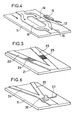
- FIGS. 2A and 2B These different methods give plane light wave guides having the structure shown in FIGS. 2A and 2B.
- the propagation layer 3A of index n,> n o is limited laterally by the confinement bands 5A, 5B of index n 3 ⁇ n "which separate it from the edges 3B, 3C, of the same index n ,.
- the layer 3A is covered by the upper layer 4 of index n 2 ⁇ n 1 .
- the light radiation circulating in the propagation layer perpendicular to the plane of FIG. 2A and parallel to that of FIG. 2B is represented by the arrows 6.
- FIG. 3 represents a waveguide element ensuring a division of the light beam 6.
- the propagation layer 3A is divided into two branches 7, 8, both delimited by the confinement bands 5A, 5B and 9, 10.
- the propagation layer is divided into two branches 12, 13.
- the branch 13 comprises a deposit of zinc oxide 14 whose index is controlled by the electrode metallic 15 deposited by vacuum projection.
- the optical signal being divided into two branches, and that passing through the branch 13 being able to be electrically controlled, one can obtain in the continuation 16 of the waveguide a phase shift of one half of the optical signal, which can be added or subtract from the other half.
- An amplitude attenuator or modulator is thus obtained controlled by an electric voltage.
- the branches 22, 23 of the propagation layer are provided by etching of closely spaced streaks 24, 25, forming a diffraction grating.
- the waveguide element 31 of FIG. 6 is provided with a photodiode 32. This can be emitting or receiving, and can be coupled to a waveguide by drilling or by local deposition of gallium arsenide or indium phosphide.
- the photodiode is controlled using the metallized strip 33.
- the propagation layer is divided into two branches 34, 35.
Landscapes
- Chemical & Material Sciences (AREA)
- Engineering & Computer Science (AREA)
- Geochemistry & Mineralogy (AREA)
- Life Sciences & Earth Sciences (AREA)
- Physics & Mathematics (AREA)
- Chemical Kinetics & Catalysis (AREA)
- General Chemical & Material Sciences (AREA)
- Materials Engineering (AREA)
- Organic Chemistry (AREA)
- General Physics & Mathematics (AREA)
- Optics & Photonics (AREA)
- Microelectronics & Electronic Packaging (AREA)
- Optical Integrated Circuits (AREA)
- Surface Treatment Of Glass (AREA)
- Silicon Compounds (AREA)
Claims (5)
Applications Claiming Priority (2)
| Application Number | Priority Date | Filing Date | Title |
|---|---|---|---|
| FR8216674A FR2534034B1 (fr) | 1982-10-05 | 1982-10-05 | Guide d'ondes lumineuses, et procedes de fabrication de celui-ci |
| FR8216674 | 1982-10-05 |
Publications (2)
| Publication Number | Publication Date |
|---|---|
| EP0106752A1 EP0106752A1 (de) | 1984-04-25 |
| EP0106752B1 true EP0106752B1 (de) | 1988-05-18 |
Family
ID=9277984
Family Applications (1)
| Application Number | Title | Priority Date | Filing Date |
|---|---|---|---|
| EP83401927A Expired EP0106752B1 (de) | 1982-10-05 | 1983-09-30 | Verfahren zur Herstellung von Lichtwellenleitern |
Country Status (7)
| Country | Link |
|---|---|
| US (1) | US4676820A (de) |
| EP (1) | EP0106752B1 (de) |
| JP (1) | JPS59501662A (de) |
| CA (1) | CA1244302A (de) |
| DE (1) | DE3376646D1 (de) |
| FR (1) | FR2534034B1 (de) |
| WO (1) | WO1984001366A1 (de) |
Families Citing this family (27)
| Publication number | Priority date | Publication date | Assignee | Title |
|---|---|---|---|---|
| FR2576693B1 (fr) * | 1985-01-30 | 1989-02-17 | Comp Generale Electricite | Procede de fabrication d'un composant optique a gradient d'indice de refraction |
| FR2578986B1 (fr) * | 1985-03-15 | 1987-04-10 | Commissariat Energie Atomique | Transducteur opto-electronique integre et son procede de fabrication |
| GB8515814D0 (en) * | 1985-06-21 | 1985-07-24 | British Telecomm | Fabrication of optical waveguides |
| US4911712A (en) * | 1988-04-14 | 1990-03-27 | Heraeus Lasersonics, Inc. | Medical laser probe |
| US5196041A (en) * | 1991-09-17 | 1993-03-23 | The Charles Stark Draper Laboratory, Inc. | Method of forming an optical channel waveguide by gettering |
| US5178658A (en) * | 1991-09-17 | 1993-01-12 | The Charles Stark Draper Laboratory, Inc. | Method for forming an optical waveguide by selective volatization |
| US5194079A (en) * | 1991-09-17 | 1993-03-16 | The Charles Stark Draper Laboratory, Inc. | Method of forming an optical channel waveguide by thermal diffusion |
| IT1250320B (it) * | 1991-10-15 | 1995-04-07 | Sip | Procedimento per la fabbricazione di guide ottiche attive a striscia monomodali per telecomunicazioni ottiche |
| JP3203178B2 (ja) * | 1996-02-27 | 2001-08-27 | 日立電線株式会社 | 光導波路、光モジュール及び光システム |
| US5938811A (en) * | 1997-05-23 | 1999-08-17 | Lucent Technologies Inc. | Method for altering the temperature dependence of optical waveguides devices |
| GB2369820B (en) * | 2000-12-08 | 2003-04-23 | Univ Southampton | Fabrication of substrates for planar waveguide devices and planar waveguide devices |
| AU2002309629A1 (en) * | 2001-05-04 | 2002-11-18 | L3 Optics, Inc. | Method and apparatus for detecting and latching the position of a mems moving member |
| US6947651B2 (en) * | 2001-05-10 | 2005-09-20 | Georgia Tech Research Corporation | Optical waveguides formed from nano air-gap inter-layer dielectric materials and methods of fabrication thereof |
| US7115321B2 (en) * | 2002-07-26 | 2006-10-03 | Kimberly-Clark Worldwide, Inc. | Absorbent binder coating |
| US6808801B2 (en) | 2002-07-26 | 2004-10-26 | Kimberly-Clark Worldwide, Inc. | Absorbent article with self-forming absorbent binder layer |
| US6887961B2 (en) * | 2002-07-26 | 2005-05-03 | Kimberly-Clark Worldwide, Inc. | Absorbent binder composition and method of making it |
| US6964803B2 (en) * | 2002-07-26 | 2005-11-15 | Kimberly-Clark Worldwide, Inc. | Absorbent structures with selectively placed flexible absorbent binder |
| US6737491B2 (en) * | 2002-07-26 | 2004-05-18 | Kimberly-Clark Worldwide, Inc. | Absorbent binder composition and method of making same |
| US6822135B2 (en) * | 2002-07-26 | 2004-11-23 | Kimberly-Clark Worldwide, Inc. | Fluid storage material including particles secured with a crosslinkable binder composition and method of making same |
| US7205259B2 (en) * | 2002-07-26 | 2007-04-17 | Kimberly-Clark Worldwide, Inc. | Absorbent binder desiccant composition and articles incorporating it |
| US7378566B2 (en) * | 2002-12-13 | 2008-05-27 | Kimberly-Clark Worldwide, Inc. | Absorbent core including folded substrate |
| US7294591B2 (en) * | 2002-12-13 | 2007-11-13 | Kimberly-Clark Worldwide, Inc. | Absorbent composite including a folded substrate and an absorbent adhesive composition |
| US20070083175A1 (en) * | 2005-10-11 | 2007-04-12 | Kimberly-Clark Worldwide, Inc. | Transparent/translucent absorbent composites and articles |
| US7619131B2 (en) * | 2005-12-02 | 2009-11-17 | Kimberly-Clark Worldwide, Inc. | Articles comprising transparent/translucent polymer composition |
| US7312286B2 (en) * | 2005-12-02 | 2007-12-25 | Stockhausen, Inc. | Flexible superabsorbent binder polymer composition |
| US20070129697A1 (en) * | 2005-12-02 | 2007-06-07 | Soerens Dave A | Articles comprising flexible superabsorbent binder polymer composition |
| US7335713B2 (en) | 2005-12-02 | 2008-02-26 | Stockhausen, Inc. | Method for preparing a flexible superabsorbent binder polymer composition |
Family Cites Families (11)
| Publication number | Priority date | Publication date | Assignee | Title |
|---|---|---|---|---|
| US3134689A (en) * | 1961-03-24 | 1964-05-26 | Intellux Inc | Thin film structure and method of making same |
| DE2313202C2 (de) * | 1972-03-30 | 1985-09-05 | Corning Glass Works, Corning, N.Y. | Optischer Wellenleiter |
| US3884336A (en) * | 1973-04-16 | 1975-05-20 | Robert W Williamson | Safety mechanism for presses, machines and fixtures |
| US4153328A (en) * | 1974-05-13 | 1979-05-08 | The Regents Of The University Of California | Polarization converter and circuit elements for use in optical waveguides |
| US4116530A (en) * | 1976-07-29 | 1978-09-26 | Texas Instruments Incorporated | Optical waveguides grown by selective liquid phase epitaxy |
| US4111521A (en) * | 1977-01-21 | 1978-09-05 | Xerox Corporation | Semiconductor light reflector/light transmitter |
| US4243398A (en) * | 1978-02-09 | 1981-01-06 | Nippon Electric Co., Ltd. | Method of producing dielectric diffraction gratings or dielectric multilayer interference filters |
| US4262995A (en) * | 1979-03-05 | 1981-04-21 | Hughes Aircraft Company | Planar star coupler device for fiber optics |
| US4425146A (en) * | 1979-12-17 | 1984-01-10 | Nippon Telegraph & Telephone Public Corporation | Method of making glass waveguide for optical circuit |
| JPS5781213A (en) * | 1980-11-11 | 1982-05-21 | Nippon Telegr & Teleph Corp <Ntt> | Production of thin film for optical waveguide |
| NL8006410A (nl) * | 1980-11-25 | 1982-06-16 | Philips Nv | Werkwijze voor de vervaardiging van geintegreerde optische golfgeleider circuits en circuits verkregen met deze werkwijze. |
-
1982
- 1982-10-05 FR FR8216674A patent/FR2534034B1/fr not_active Expired
-
1983
- 1983-09-30 EP EP83401927A patent/EP0106752B1/de not_active Expired
- 1983-09-30 DE DE8383401927T patent/DE3376646D1/de not_active Expired
- 1983-10-05 CA CA000438369A patent/CA1244302A/fr not_active Expired
- 1983-10-05 JP JP83503148A patent/JPS59501662A/ja active Pending
- 1983-10-05 WO PCT/FR1983/000201 patent/WO1984001366A1/fr not_active Ceased
-
1986
- 1986-02-19 US US06/831,112 patent/US4676820A/en not_active Expired - Fee Related
Also Published As
| Publication number | Publication date |
|---|---|
| WO1984001366A1 (fr) | 1984-04-12 |
| US4676820A (en) | 1987-06-30 |
| FR2534034A1 (fr) | 1984-04-06 |
| FR2534034B1 (fr) | 1986-02-28 |
| JPS59501662A (ja) | 1984-10-04 |
| EP0106752A1 (de) | 1984-04-25 |
| CA1244302A (fr) | 1988-11-08 |
| DE3376646D1 (en) | 1988-06-23 |
Similar Documents
| Publication | Publication Date | Title |
|---|---|---|
| WO1984001366A1 (fr) | Procede de fabrication de guides d'ondes lumineuses | |
| JP3325825B2 (ja) | 3次元周期構造体及びその作製方法並びに膜の製造方法 | |
| EP0681197B1 (de) | Optoelektronische Halbleitervorrichtung mit einem integrierten Modenanpassungselement | |
| EP0219401A1 (de) | Differentieller Absorptionspolarisator, Verfahren und Vorrichtung für seine Herstellung | |
| FR2548393A1 (fr) | Dispositif polariseur optique integre et son procede de fabrication | |
| EP0285499B1 (de) | Verfahren zur lokalen Erhöhung des Brechungsindizes eines elektrooptischen, in geführter Wellenleiteroptik zu verwendenden Materials und nach diesem Verfahren hergestelltes Material | |
| US20010021293A1 (en) | Method for modifying refractive index in optical wave-guide device | |
| FR2486250A1 (fr) | Guide d'ondes en verre pour circuit optique et procede de fabrication | |
| EP0442779A1 (de) | Integriert-optischer Wellenleiter und Herstellungsverfahren | |
| US4329016A (en) | Optical waveguide formed by diffusing metal into substrate | |
| EP0199638B1 (de) | Verfahren zur Herstellung auf einem Isoliersubstrat eines gerichteten einkristallinen Siliziumfilms mit lokalisierten Fehlern | |
| FR2791781A1 (fr) | Filtre polarisant et son procede de fabrication | |
| US4206251A (en) | Method for diffusing metals into substrates | |
| EP1121732A1 (de) | Planarer wellenleiterlaserverstärker | |
| FR2507834A1 (fr) | Laser a semiconducteurs stabilise | |
| FR2548220A1 (fr) | Guide d'onde lumineuse sur materiau semi-conducteur | |
| US5491768A (en) | Optical waveguide employing modified gallium arsenide | |
| FR2951740A1 (fr) | Procede de realisation d'un cristal magneto-photonique, cristal magneto-photonique et composant comprenant un tel cristal. | |
| FR2713350A1 (fr) | Composant optique à pluralité de réseaux de bragg et procédé de fabrication de ce composant. | |
| US4067641A (en) | Waveguide for integrated optical circuits | |
| CA2243864C (fr) | Procede de fabrication de reseaux a longs pas dans les fibres optiques | |
| EP0202977B1 (de) | Verfahren zur Herstellung auf einem Isoliersubstrat eines gerichteten einkristallinen Siliziumfilms mit lokalisierten Fehlern | |
| JPH01315707A (ja) | 電磁放射結合デバイス | |
| FR2574566A1 (fr) | Diodes emettrices/receptrices de lumiere et elements de transmission optiques non reciproques integres, et leur procede de fabrication | |
| Hunsperger | Waveguide fabrication techniques |
Legal Events
| Date | Code | Title | Description |
|---|---|---|---|
| PUAI | Public reference made under article 153(3) epc to a published international application that has entered the european phase |
Free format text: ORIGINAL CODE: 0009012 |
|
| AK | Designated contracting states |
Designated state(s): CH DE FR GB IT LI NL SE |
|
| 17P | Request for examination filed |
Effective date: 19841016 |
|
| 17Q | First examination report despatched |
Effective date: 19860714 |
|
| D17Q | First examination report despatched (deleted) | ||
| GRAA | (expected) grant |
Free format text: ORIGINAL CODE: 0009210 |
|
| AK | Designated contracting states |
Kind code of ref document: B1 Designated state(s): CH DE FR GB IT LI NL SE |
|
| REF | Corresponds to: |
Ref document number: 3376646 Country of ref document: DE Date of ref document: 19880623 |
|
| ITF | It: translation for a ep patent filed | ||
| GBT | Gb: translation of ep patent filed (gb section 77(6)(a)/1977) | ||
| PLBE | No opposition filed within time limit |
Free format text: ORIGINAL CODE: 0009261 |
|
| STAA | Information on the status of an ep patent application or granted ep patent |
Free format text: STATUS: NO OPPOSITION FILED WITHIN TIME LIMIT |
|
| 26N | No opposition filed | ||
| ITTA | It: last paid annual fee | ||
| PGFP | Annual fee paid to national office [announced via postgrant information from national office to epo] |
Ref country code: GB Payment date: 19940823 Year of fee payment: 12 |
|
| PGFP | Annual fee paid to national office [announced via postgrant information from national office to epo] |
Ref country code: CH Payment date: 19940921 Year of fee payment: 12 |
|
| PGFP | Annual fee paid to national office [announced via postgrant information from national office to epo] |
Ref country code: SE Payment date: 19940922 Year of fee payment: 12 |
|
| PGFP | Annual fee paid to national office [announced via postgrant information from national office to epo] |
Ref country code: FR Payment date: 19940929 Year of fee payment: 12 |
|
| PGFP | Annual fee paid to national office [announced via postgrant information from national office to epo] |
Ref country code: NL Payment date: 19940930 Year of fee payment: 12 Ref country code: DE Payment date: 19940930 Year of fee payment: 12 |
|
| EAL | Se: european patent in force in sweden |
Ref document number: 83401927.5 |
|
| PG25 | Lapsed in a contracting state [announced via postgrant information from national office to epo] |
Ref country code: LI Effective date: 19950930 Ref country code: GB Effective date: 19950930 Ref country code: CH Effective date: 19950930 |
|
| PG25 | Lapsed in a contracting state [announced via postgrant information from national office to epo] |
Ref country code: SE Effective date: 19951001 |
|
| PG25 | Lapsed in a contracting state [announced via postgrant information from national office to epo] |
Ref country code: NL Effective date: 19960401 |
|
| REG | Reference to a national code |
Ref country code: CH Ref legal event code: PL |
|
| GBPC | Gb: european patent ceased through non-payment of renewal fee |
Effective date: 19950930 |
|
| PG25 | Lapsed in a contracting state [announced via postgrant information from national office to epo] |
Ref country code: FR Effective date: 19960531 |
|
| PG25 | Lapsed in a contracting state [announced via postgrant information from national office to epo] |
Ref country code: DE Effective date: 19960601 |
|
| NLV4 | Nl: lapsed or anulled due to non-payment of the annual fee |
Effective date: 19960401 |
|
| EUG | Se: european patent has lapsed |
Ref document number: 83401927.5 |
|
| REG | Reference to a national code |
Ref country code: FR Ref legal event code: ST |