EP0106511A2 - Gap control system for localized vacuum processing - Google Patents
Gap control system for localized vacuum processing Download PDFInfo
- Publication number
- EP0106511A2 EP0106511A2 EP83305270A EP83305270A EP0106511A2 EP 0106511 A2 EP0106511 A2 EP 0106511A2 EP 83305270 A EP83305270 A EP 83305270A EP 83305270 A EP83305270 A EP 83305270A EP 0106511 A2 EP0106511 A2 EP 0106511A2
- Authority
- EP
- European Patent Office
- Prior art keywords
- gap
- workpiece
- envelope
- tip
- vacuum
- Prior art date
- Legal status (The legal status is an assumption and is not a legal conclusion. Google has not performed a legal analysis and makes no representation as to the accuracy of the status listed.)
- Withdrawn
Links
Images


Classifications
-
- H—ELECTRICITY
- H01—ELECTRIC ELEMENTS
- H01J—ELECTRIC DISCHARGE TUBES OR DISCHARGE LAMPS
- H01J37/00—Discharge tubes with provision for introducing objects or material to be exposed to the discharge, e.g. for the purpose of examination or processing thereof
- H01J37/30—Electron-beam or ion-beam tubes for localised treatment of objects
-
- H—ELECTRICITY
- H01—ELECTRIC ELEMENTS
- H01L—SEMICONDUCTOR DEVICES NOT COVERED BY CLASS H10
- H01L21/00—Processes or apparatus adapted for the manufacture or treatment of semiconductor or solid state devices or of parts thereof
- H01L21/67—Apparatus specially adapted for handling semiconductor or electric solid state devices during manufacture or treatment thereof; Apparatus specially adapted for handling wafers during manufacture or treatment of semiconductor or electric solid state devices or components ; Apparatus not specifically provided for elsewhere
- H01L21/68—Apparatus specially adapted for handling semiconductor or electric solid state devices during manufacture or treatment thereof; Apparatus specially adapted for handling wafers during manufacture or treatment of semiconductor or electric solid state devices or components ; Apparatus not specifically provided for elsewhere for positioning, orientation or alignment
Definitions
- This invention relates to vacuum processing of a workpiece and, more particularly, to systems for controlling a gap between the tip of a vacuum envelope apparatus and a surface of a workpiece in a localized vacuum processing system.
- Particle beam systems such as ion implanters, electron beam lithography systems and ion beam lithography systems, require evacuation of the region along the path between the particle beam source and the workpiece being treated.
- Various types of vacuum processing chambers have been used. In the simplest, workpieces are loaded either singly or in a batch into a work chamber containing the particle beam source. After loading, the chamber is sealed and is vacuum pumped until the desired level of vacuum is achieved. This approach is relatively slow, since the entire volume of the work chamber must be vacuum pumped each time a new batch of workpieces is introduced. Additional problems include outgassing of absorbed gases and introduction of contaminants. In many processes, for example, commercial semiconductor processing, throughput is of utmost Importance.
- air locks have been used for introducing the workpiece into the processing chamber.
- the workpiece is introduced into a small volume which is then sealed and vacuum pumped.
- a door or valve connecting the air lock to the processing chamber is opened.
- the vacuum pumping time is reduced by reducing the volume to be pumped.
- Certain particle beam processes such as electron beam lithography, require movement of the workpiece during processing.
- electron beam lithography microminiature patterns of extremely high accuracy are exposed on the workpiece.
- the deflection field of the electron beam is limited to an area much smaller than the area of the workpiece.
- the deflection field in an electron beam system is one or a few millimeters, while the workpiece, usually a semiconductor wafer or a mask plate, can be up to several inches in dimension.
- precise positioning of the workpiece is required.
- the workpiece has been positioned by a system of drive motors external to the vacuum region and a mechanical linkage has been used to transmit the motion into the vacuum through bellows or rotary vacuum seals.
- Such systems have been large, complex and relatively unreliable.
- the particle beam is scanned over a very small localized region of the workpiece surface at any given time.
- the vacuum processing apparatus includes an envelope which defines an internal vacuum processing zone.
- the tip of the envelope is positioned just above the surface of the workpiece and is spaced from the workpiece by a preselected gap.
- the tip of the envelope together with the workpiece forms a non-contacting graded vacuum seal between the internal vacuum processing zone and the ambient environment.
- the envelope tip typically has the general shape of a cone and provides a vacuum zone on the surface of the workpiece which is small in. comparison with the size of the workpiece.
- stage speeds of between 1 and 10 cm/second are typically employed.
- the gap between the tip of the envelope and the workpiece must be dynamically controlled within specified limits. If the gap becomes too large, the vacuum in the vacuum zone is reduced, and processing is interrupted until the required vacuum level can again be achieved.
- Electron beam columns used in lithography systems must be operated in the mid to high vacuum range, and, typically, inadequate space is available to provide high conductance vacuum pumping. In such cases, the gap must be relatively small.
- workpieces such as semiconductor wafers are in general flat and planar, they are subject to thickness variations, surface irregularities and warping, all of which can cause gap variations during the lateral movement of the wafer.
- stage system which provides the lateral movement of the wafer with respect to the tip of the envelope, is subject to certain imperfections and tolerances which can cause'the gap to vary as the wafer is moved. These factors make it necessary to dynamically control the gap between the tip of the envelope and the workpiece during processing.
- an object of the present invention to provide apparatus for controlling the gap between a localized vacuum processing envelope and a surface of a workpiece.
- the apparatus comprises sensing means operative to provide a gap sense signal corresponding to the measured gap between the envelope apparatus and the workpiece.
- a control means is operative in response to the gap sense signal to provide a control signal representative of the difference between the measured gap and a required gap dimension or range of allowed dimensions.
- An actuating means is operative to vary the gap between the envelope apparatus and the workpiece in response to the control signal so as to reduce the difference between the measured gap and the required gap dimension or range of allowed dimensions.
- the actuating means includes three independently controlled actuators coupled through a workpiece holder to the workpiece, and the control means provides independent actuator signals to each of the actuators.
- the actuating means thereby has the capability to vary the gap and to vary the angle between the plane of the workpiece surface and the envelope apparatus.
- the localized vacuum envelope apparatus includes an envelope which defines an internal vacuum processing zone, a generally planar tip and a plurality of vacuum pumping stages.
- the sensing means includes pressure sensing means operative to provide a pressure reading corresponding to the pressure in one of the stages and representative of the measured gap between the tip and the workpiece.
- apparatus for localized vacuum processing of a generally planar workpiece includes a vacuum envelope apparatus as described above, means for moving the workpiece laterally with respect to the envelope apparatus and means for controlling the gap between the tip and the workpiece.
- the gap control means includes a source of gas under pressure coupled to a plurality of holes spaced around the periphery of the tip of the envelope apparatus. A gas bearing is formed between the tip and the workpiece and the gap is determined by the pressure of the gas.
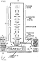
- An electron beam lithography system includes a localized vacuum envelope apparatus 10 mounted to the output of an electron beam column 12 which includes an electron source, illumination and shaping optics, demagnification optics and projection and deflection optics.
- An electron beam column 12 is described in pending application Serial No. 354,822, filed March 4, 1982. Other suitable electron beam columns are known in the art.
- the output of the column 12 is a finely focused electron beam 14 which passes through the envelope apparatus 10 and impinges on a workpiece such as a semiconductor wafer 16.
- the entire region traversed by the electron beam 14 between the electron source and the wafer 16 is maintained at high vacuum, on the order of 1 0- 6 Torr, by a high vacuum pump 17 coupled to the column 12. It will be understood by those skilled in the art that in a practical system, the electron optical elements are located outside the vacuum region and a central tube traversed by the electron beam 14 is maintained at high vacuum.
- the envelope apparatus 10 is coupled to a first stage vacuum pump 20 and to a second stage vacuum pump 22.
- the wafer 16 is supported and held in position by a vacuum chuck 18 which is supported above a movable stage 24 by actuators 26, 28, 30 and a flexible ring. Wafers are placed on the vacuum chuck 18 and removed therefrom by an automated wafer handling system 31.
- the stage 24 is movably supported on a planar surface 32 by an air bearing and is translated over the surface 32 by an x-axis drive system 34 and a y-axis drive system 35.
- the position of the stage 24 and the wafer 16 on the plane 32 is sensed by" an x position sensor 36 and a y position sensor 37, which are typically laser interferometers.
- the x and y axes define the plane 32 while the z-axis coincides generally with the path of the electron beam 14.
- the complete electron beam lithography system further includes a controller, or computer and associated electronic system (not shown in FIG. 1), which controls the column 12, the drive system 34, 35, the vacuum system and the wafer handling system 17 and which stores pattern data and provides beam control signals.
- the envelope apparatus 10 includes an envelope 40 which can be conical in shape and includes a generally planar tip 42.
- the tip 42 is positioned during processing slightly above the wafer 16.
- the envelope 40 defines a vacuum processing zone 44 on the surface of the wafer 16.
- a differential pumping arrangement forms during operation a graded vacuum seal between the vacuum zone 44 and the ambient environment.
- the tip 42 includes annular apertures 46, 48 concentric with the vacuum zone 44.
- the annular aperture 48 is coupled to the first stage vacuum pump 20 which reduces the pressure around the vacuum zone 44 to a low vacuum level.
- the annular aperture 46 is coupled to the second stage vacuum pump 22 which reduces the pressure around the vacuum zone 44 to an intermediate vacuum level.
- the vacuum zone 44 is coupled directly to the vacuum region of the electron beam column 12 and is pumped to high vacuum by the vacuum pump 17. Depending on the pressure required in a particular process, more or fewer vacuum pumping stages can be utilized to form the graded seal. To increase the vacuum conductance to the pump 17 and thereby further reduce the pressure in the vacuum zone 44, a direct connection can be made between the vacuum zone 44 and the vacuum pump 17.
- a high vacuum is maintained in the vacuum zone 44, as the envelope apparatus moves over the surface of the wafer 16.
- the electron beam is scanned over a region of the wafer surface within the vacuum zone 44. Additional information on the localized envelope apparatus 10 is given in pending application assignee's docket no. 82-19.
- the vacuum chuck 18 holds the wafer in a fixed lateral position with respect to the stage 24.
- Vacuum chucks are generally known for holding semiconductor wafers and have the advantage that physical contact is made at the rear of the wafer where damage is less likely.
- the vacuum chuck 18 must hold the wafer 16 flat during processing and must not permit any movement of the wafer 16.
- a suitable vacuum chuck includes a plurality of small pins surrounded by a rim which forms a vacuum seal with the wafer. The pins are coplanar with the top surface of the rim. When the volume behind the wafer is evacuated, the wafer is drawn into contact with the pins and thus flattened.
- the vacuum chuck 18 includes a flexible ring 56 around its outer periphery.
- the flexible ring 56 is coupled to the stage 24 so as to permit a small amount of vertical, or z-axis, motion of the vacuum chuck 18, but to prevent any lateral movement in the xy plane. Inadvertent lateral displacement of the vacuum chuck 18 relative to laser mirrors integral to the stage 24 would result in an error in the xy position of the wafer 16 during processing.
- a film of air forms an air bearing between the stage 24 and the planar surface 32 and provides relatively frictionless and particulate free movement of the stage 24 over the surface 32.
- the air bearing can be in the form of a plurality of small holes in either the stage 24 or the surface 32. Air is pumped through each of the holes at a constant rate so as to provide a cushion of air between the two surfaces.
- the actuators 26, 28, 30 provide a small amount of z-axis motion of the vacuum chuck 18 and can be independently controlled.
- the actuators 26, 28, 30 are controlled by a gap control circuit 60, as described hereinafter.
- An alignment pad 62 is mounted to the stage 24 and has a top surface which is coplanar with the top surface of the wafer 16.
- the alignment pad 62 typically includes fiducial marks (not shown) for measurement and adjustment of the electron beam 14, prior to electron beam exposure of the wafer 16.
- a Faraday cup with an alignment grid can be provided for beam adjustment.
- the drive system 34, 35 can be any suitable, highly precise xy positioning system.
- a suitable drive system 34, 35 employs linear motors, as described in pending application assignee's docket no.
- Another suitable drive system 34, 35 employs x and y drive motors coupled to the stage 24 by an arrangement of ball screws, as is known in the art. Since the stage 24 is not in vacuum, no bellows or other vacuum interface is required. The lateral position of the stage 24 is precisely sensed by the laser interferometers 36, 37, which direct laser beams at mirrors 66 polished on two perpendicular surfaces of the stage 24, as described in U.S. Patent No. 4,280,054. The output signals from the laser interferometers 36, 37 are fed to a system controller 68 which is typically a computer.
- the system controller 68 monitors the position of the stage 24 and sends control signals to the drive system 34, 35 which continuously positions the wafer 16 for electron beam exposure.
- the use of laser interferometers to monitor the xy position of a movable stage is disclosed in U.S. Patent No. 4,063,103 issued Dec. 13, 1977 to Sumi.
- the gap between the tip 42 of the envelope apparatus 10 and the surface of the wafer 16 is measured by one or more gap sensors on a continuous basis and is dynamically controlled so as to maintain a required gap dimension or range of allowed dimensions.
- physical contact between the tip 42 and the wafer 16 is highly likely to damage the microminiature devices on the surface of the wafer 16 or to crack the wafer material.
- the gap becomes too large, the pressure in the vacuum zone 44 increases due to increased air flow through the gap and becomes too high to carry on electron beam exposure of the wafer 16.
- a capacitive gap sensor 70 is mounted on the envelope 40 as close to the tip 42 as possible and directed at the wafer 16.
- a vacuum gauge 72 is coupled to the second stage of the differential pumping arrangement surrounding the vacuum zone 44 and is used in a novel manner to sense the gap between the tip 42 and the surface of the wafer 16, as described hereinafter.
- the outputs of the capacitive gap sensor 70 and the vacuum gauge 72 are coupled to the gap control circuit 60 and provide signals corresponding to the instantaneous measured gap for control purposes.
- gap sensors can be utilized in the system of FIGS. 1 and 2, depending on the required speed of operation and the type of vacuum processing being performed.
- the gap sensor must be non-contacting to avoid damage to the surface of the wafer 16.
- the gap sensor In the case of electron beam lithography, the gap sensor must have a quick response time to sense wafer surface variations during translation of the stage 24.
- the gap sensor must be sufficiently sensitive to detect gap variations of a few microns.
- Capacitive gap sensors provide good resolution and fast response time.
- the capacitive gap sensor 70 can be a Lion Precision Corp. Part No. PX305KM.
- Other suitable types of gap sensors include optical sensors, eddy current sensors and air micrometers or gauges. Optical sensors require a uniformly reflective workpiece surface to achieve accurate measurement.
- Eddy current sensors require a conductive workpiece. Air gauges have good resolution but have a relatively slow response time. A non-contacting air gauge system is sold by K Products, Inc., 453 Beacon St., Boston, Mass. A differential air servo system for controlling the position of a workpiece is described in U.S. Patent No. 3,194,055, issued July 13, 1965 to Knobel. The position of the workpiece is sensed by an air gauge.
- the vacuum gauge 72 is used as a gap sensor. It has been observed that as the gap between the tip 42 and the wafer 16 increases, the pressure in the second stage of the envelope apparatus 10 increases; and as the gap decreases, the pressure in the second stage decreases. Thus, the pressure in the second stage of the envelope apparatus 10 is directly related to the gap dimension. While the pressure does not necessarily vary linearly with gap, linearity is not required in the gap control system of the present invention. It will be understood that similar pressure variations occur in stages one and three of the envelope apparatus 10 as the gap varies. However, the pressure level in the second stage is most compatible with available vacuum gauges and demonstrates the greatest sensitivity to gap changes.
- the advantage of using the vacuum gauge 72 for gap measurement is that the gap is measured in an annular ring directly adjacent to the vacuum zone 44, the point at which the gap measurement is important. Other types of gap sensors are necessarily mounted a further distance away from the vacuum zone 44, thus giving rise to the possibility of a difference in gap between the point of measurement and the vacuum zone 44.
- the vacuum gauge 72 is operative as a gap sensor whenever the envelope apparatus 10 is over the wafer 16.
- a gap sensor such as a capacitive gap sensor is spaced from the tip 42, it can be off the edge of the wafer and useless for gap sensing even though the envelope apparatus 10 is in operating position over the wafer 16.
- a suitable vacuum gauge 72 is a capacitive manometer vacuum gauge such as MKS Instruments Inc., Part No. 222BHS-A-0.5%-10.
- FIG. 3 An example of the actuators 26, 28, 30 is shown in FIG. 3.
- the actuator must be capable of providing rapid and very precise movement. The required travel is typically very small, on the order of .005 inch.
- a piezoelectric element 76 such as as a Burleigh type PZ-44, converts an electrical signal on the order of 1,000 volts to linear mechanical motion.
- a micropositioning stage driven by a piezoelectric element is described by Scire at al in "Piezodriven 50 ⁇ m Range Stage with Subnanometer Resolution,” Rev. Sci. Instrum., 49(12), Dec. 1978, p. 1735.
- the piezoelectric element 76 is mounted at one end to a support bracket 78.
- the opposite end of the element 76 bears against one arm of a lever 80.
- the other arm of the lever 80 is coupled through a pin 82 to the vacuum chuck 18.
- the lever 80 pivots about a flexible web 84 connecting the lever 80 to a support block 86.
- the material of the flexible web 84 can be beryllium copper.
- the lengths of the arms of the lever 80 can be designed to provide the required amount of z-axis motion.
- the support block 86 and the support bracket 78 are mounted to the stage 24.
- the piezoelectric element 76 When the piezoelectric element 76 is energized by an electrical signal, it increases or decreases in length. The change in length is converted by the lever 80 into vertical, or z-axis, movement of the vacuum chuck 18. Alternatively, a Burleigh "inch worm" piezoelectric element can be utilized.
- the configuration of three actuators 26, 28, 30 shown in FIG. 3 provides the capability to raise and lower the wafer 16 along the z-axis by energizing each of the actuators 26, 28, 30 in parallel and equally. In addition, by energizing the actuators 26, 28, 30 unequally, more complex movements of the wafer 16 can be accomplished.
- the orientation of the plane of the wafer 16 can be varied in this way, since the positions of the three actuators 26, 28, 30 define the plane of the wafer 16.
- a configuration with one or two actuators can be used when adjustment of the parallelism of the wafer 16 with respect to the tip 42 is not required.
- a configuration with more than three actuators can also be used both to raise and lower arid to vary the plane of the wafer 16.
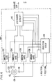
- the gap control circuit 60 processes the gap sense signals from the capacitive gap sensor 70 or the vacuum gauge 72 and provides control signals to the actuators 26, 28, 30, so as to continuously maintain a required gap dimension or range of gap dimensions between the tip 42 of the envelope apparatus 10 and the wafer 16.
- a block diagram of the gap control circuit 60 is shown in FIG. 4.
- a sensor select circuit 100 which can be an analog gating circuit, selects the signal from either the capacitive gap sensor 70 or the vacuum gauge 72, depending on the mode of operation. Typically, the signal from the capacitive gap sensor 70 is used to determine the position of the wafer before moving the wafer under the envelope apparatus, while the signal from the vacuum gauge 72 is used both in the setup mode and in the run mode.
- the capacitive gap sensor 70 is thus used as an auxiliary gap sensor for initial setup purposes.
- the selected gap sense signal is compared in a summing circuit 102 with a signal representing the required gap to provide an error signal corresponding to the difference between the measured gap and the required gap.
- the error signal is coupled to actuator control circuits 104, 106, 108.
- the actuator control circuits 104, 106, 108 also receive inputs from a gain control circuit 110 which is operative to provide independent control of each of the actuator control circuits 104, 106, 108.
- the outputs of the actuator control circuits 104, 106, 108 are coupled through actuator drivers 112, 114, 116, respectively, to the actuators 26, 28, 30.
- the actuator control circuits 104, 106, 108 function to scale the magnitude of the error signal to an appropriate level.
- the scaling, or gain control, is provided by the gain control circuit 110.
- the actuator drivers 112, 114, 116 function as interface circuits to the actuators 26, 28, 30.
- the stage 24 is initially positioned so that the tip 42 of the envelope apparatus 10 and the capacitive gap sensor 70 are above the alignment pad 62, as shown in FIG. 5A.
- the electron beam 14 is adjusted to provide the proper focus by utilizing the fiducial marks on.the alignment pad 62.
- the alignment pad 62 is a rest position for the envelope apparatus 10 and insures that vacuum is not broken in the envelope apparatus 10 during exchange of wafers.
- the alignment pad provides a stable standard for system setup and is used as a reference for initial positioning of the wafer.
- a wafer is introduced onto the vacuum chuck 18 by the automatic wafer handling system 17.
- the stage 24 is moved so that the capacitive gap sensor 70 is above the edge of the wafer 16, but the tip 42 of the envelope apparatus 10 is still located above the alignment pad 62, as shown in FIG. 5B.
- the vertical position of the wafer 16 is sensed by the capacitive gap sensor 70.
- the sensor select circuit 100 selects the capacitive gap sense signal, and the summing circuit 102 provides an error signal representative of the difference between the measured gap and the required gap.
- the gain control circuit 110 receives x position and y position signals from the system controller 68, indicating that the sensor 70 is positioned above the edge of the wafer 16 and the envelope apparatus 10 is above the alignment pad 62.
- the actuators 26, 28, 30 are energized in parallel by equal control signals, and the wafer 16 is moved up or down until the measured gap agrees with the required gap and the error signal is zero.
- the top surface of the wafer 16 adjacent the alignment pad 62 is coplanar within allowable limits with the top surface of the alignment pad 62, and the wafer 16 can be moved under the tip 42 of the envelope apparatus 10 without contacting the tip 42 or breaking vacuum. However, the remainder of the wafer 16 remains to be aligned with respect to the tip 42. Although the edge of the wafer 16 adjacent the alignment pad 62 has been properly positioned, the plane of the wafer 16 can be inclined at an unknown angle with respect to the xy plane which is parallel to the plane of stage translation and the plane of the tip 42.
- the wafer 16 is moved with respect to the envelope apparatus 10 in a pattern indicated by the dotted lines A, B, C in FIG. 5B.
- the vacuum gauge 72 be utilized for gap sensing, although the capacitive gap sensor 70 can be used.
- Path A traverses a line between the actuator 30 and the actuator 28. As Path A is traversed, the gap is monitored, and the gain control circuit 110 enables the actuator control circuit 106. The actuator 28 is energized and raises or lowers the portion of the wafer 16 thereabove so as to maintain the required gap.
- the Path B traverses a line between the actuator 28 and the actuator 26.
- Path C traverses a line between the actuator 26 and the actuator 30.
- the actuator 30 can be energized to provide further fine adjustments of the position of the wafer 16.
- the entire surface of the wafer 16 should be parallel with the plane of the tip 42 and spaced by the required gap, except for localized variations in the surface of the wafer. If necessary, the. Paths A, B, C can again be traversed to check the positioning of the wafer 16 and make further fine adjustments.
- the above setup procedure may or may not be required. It will further be understod that for larger or smaller wafers, the Paths A, B, C do not necessarily pass directly over the actuators 26, 28, 30. Any triangular path is suitable.
- the stage 24 is moved by the drive system 34, 35 back and forth beneath the envelope apparatus 10, in a prescribed pattern that eventually covers the entire surface of the wafer 16.
- the stage 24 is typically moved continuously to avoid the overhead times associated with starting and stopping. However, it will be realized that the system can be operated in a step-and-repeat mode in which the stage 24 is moved intermittently..
- the vacuum gauge 72 for gap sensing. Thus, the vacuum gap sense signal is selected by the sensor select circuit 100.
- the gain control circuit 110 provides equal gain control signals to each of the actuator control circuits 104, 106, 108.
- the gap control circuit described hereinabove compares the gap sense signal with a fixed-value required gap, it will be understood that in some applications a range of gap dimensions can be tolerated, for example, 20 ⁇ m to 40 ⁇ m.
- the gap sense signal is compared with upper and lower limits, and the actuators 26, 28, 30 are energized when the measured gap is outside these limits.
- an alarm signal can be sent to the controller 68 and corrective action can be taken.
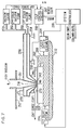
- Gap sensing is accomplished by capacitive gap sensors 120, 122, 124, 126 positioned at 90 degree intervals around the tip 42 of the envelope apparatus 10. A top view of such an arrangement is shown in FIG. 6.
- Each of the capacitive gap sensors 120, 122, 124, 126 individually senses the gap between the tip 42 and the wafer 16 and provides a gap sense signal. Depending on the orientation and surface contour of the wafer 16, the four gap sense signals may or may not be equal.
- the gap sense signals from the gap sensors 120, 122, 124, 126 can be processed in various ways to control the actuators 26, 28, 30. An example of such processor is illustrated in FIG. 6.
- a sensor processor 130 includes analog gates 132, 134, 136, 138 which receive gap sense signals from the gap sensors 120, 122, 124, 126, respectively.
- the analog gates 132, 134, 136, 138 are controlled by the outputs of a position logic circuit 140 which operates as described below.
- the outputs of the analog gates 132, 134, 136, 138 are connected to an averaging circuit 142 which calculates an average value of the gap between the tip 42 and the wafer 16.
- the outputs of the position logic circuit 140 are also connected to the averaging circuit 142.
- the position logic circuit 140 receives x and y position information from the system controller 68. Referring again to FIG. 4, the sensor select circuit 100 is replaced in the present embodiment by the sensor processor 130 of FIG. 6.
- the average gap signal from the sensor processor 130 is coupled to the summing circuit 102 of FIG. 4, which calculates an error signal as described hereinabove.
- the embodiment of FIG. 6 can employ the same initial setup procedure described hereinabove in connection with FIGS. 1-5, except that the gap sensors 120, 122, 124, 126 perform all gap sensing.
- the alignment pad 62 is positioned under the tip 42 during the exchange of wafers. Then the wafer 16 is positioned under the tip 42 and the Path A, B, C, as illustrated in FIG. 5B, is traversed.
- the gap sensors 120, 122, 124, 126 monitor the gap, and the wafer is dynamically positioned so as to establish parallelism between the wafer 16 and the tip 42 and to establish the required gap.
- the capacitive gap sensors 120, 122, 124, 126 monitor the gap as the wafer 16 is moved back and forth under the envelope apparatus 10. When the central portion of the wafer 16 is being exposed, all of the gap sensors 120, 122, 124, 126 are over the wafer 16. However, it will be realized that when the edge of the wafer 16 is being exposed, one or two of the gap sensors 120, 122, 124, 126 will be off the edge of the wafer 16. Gap sense signals from any of the gap sensors not over the wafer 16 should be ignored in the averaging process.
- the position logic circuit 140 determines the relative positions of the tip 42 and the wafer 16 and enables appropriate ones of the analog gates 132, 134, 136, 138.
- the position logic circuit 140 can be in the form of threshold detection circuits. Thus, for example, when the x position exceeds a given positive value, the appropriate analog gate is inhibited, and the corresponding sensor signal is gated off. Additional threshold detection circuits detect negative values of x and positive and negative values of y so as to enable only the capacitive gap sensors which are positioned above the wafer 16. The outputs of the position logic circuit 140 control the averaging circuit 142 so that the averaging process is based on the correct number of input sensor signals.
- each of the gap sensor signals can be individually processed to obtain a dynamic measurement of parallelism as well as gap.
- the actuators 26, 28, 30 are energized so as to correct the parallelism of the wafer 16 with respect to the tip 42, as well as the gap therebetween.
- other types of gap sensors can be positioned around the tip 42, as shown in FIG. 6.
- FIG. 7 An alternative embodiment of apparatus for localized vacuum processing of a workpiece is illustrated in schematic form in FIG. 7.
- the apparatus includes a localized vacuum processing envelope apparatus 210 coupled through a bellows 211 to the output of a particle beam source, such as an electron beam column 212, which corresponds to the column 12 described hereinabove.
- An electron beam 214 passes through the envelope apparatus 210 and impinges on a semiconductor wafer 216.
- the wafer 216 is supported and held in position by a vacuum chuck 218 which in turn is mounted on a stage 224.
- the stage 224 is movably supported by an air bearing on a planar surface 232 and is translated over the surface 232 by a drive system 234.
- the envelope apparatus 210 is generally similar in construction and operation to the envelope apparatus 10 shown in FIGS. 1 and 2 and described hereinabove.
- the envelope apparatus' 210 differs from the envelope apparatus 10 in that it is movable with respect to the electron beam column 212 and includes a pivot arm 236.
- the envelope apparatus 210 includes a generally conical envelope 24 0 and a generally planar tip 242.
- the envelope 240 defines a vacuum processing zone 244 on the surface of the wafer 216.
- the envelope apparatus 210 includes annular apertures concentric with the vacuum zone 244 which are vacuum pumped through the pivot arm 236 by vacuum pumps 250, 252.
- the vacuum zone 244 is coupled to the high vacuum region of the electron beam column 212 and is sealed thereto by the bellows 211.
- the envelope apparatus 210 operates the same as the envelope apparatus 10 described hereinabove to provide high vacuum in the vacuum zone 244.
- the envelope apparatus 210 pivots about a pivot point 254 so as to permit a small amount of substantially vertical movement.
- the envelope apparatus 210 is controlled in its movement about the pivot point 254 by an actuator 258.
- the vacuum chuck 218 operates the same as the vacuum chuck 18, shown in FIG. 1 and described hereinabove, to hold the wafer in a fixed position from its rear surface.
- the vacuum chuck 218 is rigidly mounted to the stage 224.
- An alignment pad 262 is mounted to the stage 224 and has a top surface which is coplanar with the top surface of the wafer 216.
- the drive system 234 can be any suitable highly precise xy positioning system, as described hereinabove in connection with the drive system 34, 35.
- the lateral position of the stage 224 is sensed by a laser interferometer 264 which directs a laser beam at mirrors 266 polished on two perpendicular surfaces of the stage 224. Output signals from the laser interferometer 264 are fed to a system controller 268 ' which monitors the position of the stage 224 and sends control signals to the drive system 234.
- the initial z-axis position of the wafer 216 is sensed by a capacitive gap sensor 270 mounted on the envelope 240 as close to the tip 242 as possible and directed at the wafer 216.
- a vacuum gauge 272 is coupled to the second stage of the graded seal surrounding the vacuum zone 244 and is used to sense the gap in the same manner as the vacuum gauge 72 described hereinabove.
- the outputs of the capacitive gap sensor 27 0 and the vacuum gauge 272 are coupled to a gap control circuit 260 and provide signals corresponding to the instantaneous measured gap.
- the output of the gap control circuit 260 is a control signal which energizes the actuator 258 and causes the envelope apparatus 210 to move up or down so as to maintain the required gap.
- the capacitive gap sensor 270 and the vacuum gauge 272 can be the same as the gap sensors described hereinabove in connection with FIG. 2, or suitable alternative gap sensors can be utilized.
- the actuator 258 can utilize a piezoelectric element as shown in FIG. 3.
- An example of the gap control circuit 260 is shown in block diagram form in FIG. 8.
- One of the gap sense signals is selected by a sensor select circuit 290, according to the mode of operation of the system.
- the selected gap sense signal is compared with a signal representing the required gap in a summing circuit 292 to produce an error signal representative of the difference therebetween.
- the error signal is scaled to an appropriate level by an actuator control circuit 294.
- the output of the actuator control circuit 294 is connected through an actuator driver 296 to the actuator 258.
- the stage 224 is initially positioned so that the tip 242 of the envelope apparatus 210 and the capacitive gap sensor 270 are above the alignment pad 262.
- the electron beam 214 is focused by utilizing fiducial marks on the alignment pad 262.
- a wafer is introduced onto the vacuum chuck 218 by an automatic wafer handling system.
- the stage 224 is moved so that the capacitive gap sensor 270 is above the edge of the wafer 216, and the tip 242 of the envelope apparatus 210 is above the alignment pad 262.
- the position of the wafer 216 is sensed by the gap sensor 270. Referring to FIG.
- the capacitive gap sense signal is selected by the sensor select circuit 290 and is fed to the summing circuit 292.
- the measured gap is compared with the required gap by the summing circuit 292, and an error signal representative of the difference is provided to the actuator control circuit 294.
- the actuator control circuit 294 scales the error signal to the appropriate level and provides an output signal through the actuator driver 296 to the actuator 258.
- the tip 242 is raised or lowered by a small amount to compensate for slight differences in level between the wafer 216 and the alignment pad 262. However, the tip 242 cannot be raised so much that the vacuum is broken.
- the stage 224 can then be moved so that the tip 242 is able to cross the small space between the alignment pad 262 and the wafer 216 without substantial loss of vacuum.
- the wafer 216 When the wafer 216 is not properly positioned with respect to the alignment pad 262, it can be repositioned by the wafer handling system or can be replaced. Alternatively, the system can be provided with means for causing relative vertical movement between the wafer 216 and the alignment pad 262.
- the stage 224 After the stage 224 has been moved so that the tip 242 is over the wafer 216, normal electron beam exposure of the wafer 216 can proceed.
- the stage 224 is moved by the drive system 234 back and forth beneath the envelope apparatus 210 in a prescribed pattern that eventually covers the entire surface of the wafer 216.
- the gap between the tip 242 and the wafer 216 is dynamically controlled.
- utilization of the vacuum gauge 272 is preferred for gap sensing during normal operation.
- the gap sense signal from the vacuum gauge 272 is selected by the sensor select circuit 290 and is provided to the summing circuit 292, which compares the gap sense signal with the signal representing the required gap.
- the error signal from the summing circuit 292 is scaled by the actuator control circuit 294 and is provided through the actuator driver 296 to the actuator 258.
- the actuator 258 moves the envelope apparatus upward or downward as required to maintain the required gap between the wafer 216 and the tip 242.
- the tip 242 of the envelope apparatus 210 tracks over the surface of the wafer 216, and follows variations and irregularities in the wafer surface.
- the tip 242 of the envelope apparatus 210 follows the surface of the wafer 216 to maintain the required gap therebetween.
- the wafer 216 is fixed in vertical position with respect to the electron beam column 212. Therefore, irregularities and variations in the surface of the wafer 216 cause variations in the distance between the electron beam column 212 and the wafer surface being exposed by the electron beam 214.
- Electron beam columns for high precision lithography can have a short depth of focus, on the order of a few microns. When the variations in the surface of the wafer 216 exceed this amount, dynamic focus corrections must be applied to the electron beam column 212 as the stage 224 and the wafer 216 are moved back and forth beneath the tip 242.
- the required focus correction can be determined by utilizing a gap sensor 273 which monitors the position of the envelope apparatus 210, with respect to the electron beam column 212. Since the envelope apparatus 210 tracks the surface of the wafer 216, the position of the envelope apparatus 210 indicates the position of the wafer surface at that location.
- the outer periphery of the tip 242 of the envelope apparatus 210 includes a plurality of equally spaced holes, each of which is connected to a source of air under pressure. The air is forced out through the holes into the gap between the tip 242 and the wafer 216 and forms an air bearing therebetween. A portion of the air escapes outward to the external environment, while the remainder of the air is removed by the vacuum pumping system of the envelope apparatus 210. The airflow through the holes is adjusted so that the tip 242 is spaced above the surface of the wafer 216 by the required gap. Thus, as the wafer 216 is moved beneath the tip 242, the envelope apparatus 210 rides on a cushion of air at the required gap above the wafer 216 and follows variations in the surface.
- the present invention apparatus for controlling the gap between the tip of a localized vacuum processing envelope apparatus and a workpiece so as to prevent degradation of the vacuum level in the envelope apparatus and to prevent contact between the envelope apparatus and the workpiece.
- the apparatus has the capability to control not only the spacing between the tip of the envelope apparatus and the workpiece but also the orientation of the plane of the workpiece with respect to the envelope apparatus.
- a method for sensing the gap by measuring the pressure at a specified location in the gap.
- the invention is particularly useful when the workpiece is a generally planar semiconductor wafer subject to thickness variations, surface irregularities and warping.
- a suitable wafer holder is a vacuum chuck adapted for holding the wafer by its back surface, and the actuating means preferably include a piezoelectric element operative to provide linear movement in response to actuator signals.
- the sensing means preferably includes capacitive gap sensing means positioned adjacent the tip of the envelope apparatus and preferably includes a plurality of such capacitive gap sensors, positioned around the tip.
- An alternative sensing means is an air gauge gap sensing means.
- the workpiece is preferably fixed in position along the z-axis and the actuating means moves the envelope along the z-axis.
- the envelope apparatus is preferably coupled to the output of a particle beam source.
Abstract
Description
- This invention relates to vacuum processing of a workpiece and, more particularly, to systems for controlling a gap between the tip of a vacuum envelope apparatus and a surface of a workpiece in a localized vacuum processing system.
- Particle beam systems, such as ion implanters, electron beam lithography systems and ion beam lithography systems, require evacuation of the region along the path between the particle beam source and the workpiece being treated. Various types of vacuum processing chambers have been used. In the simplest, workpieces are loaded either singly or in a batch into a work chamber containing the particle beam source. After loading, the chamber is sealed and is vacuum pumped until the desired level of vacuum is achieved. This approach is relatively slow, since the entire volume of the work chamber must be vacuum pumped each time a new batch of workpieces is introduced. Additional problems include outgassing of absorbed gases and introduction of contaminants. In many processes, for example, commercial semiconductor processing, throughput is of utmost Importance. To increase processing speed, air locks have been used for introducing the workpiece into the processing chamber. The workpiece is introduced into a small volume which is then sealed and vacuum pumped. When the desired level of vacuum is reached, a door or valve connecting the air lock to the processing chamber is opened. The vacuum pumping time is reduced by reducing the volume to be pumped.
- Certain particle beam processes, such as electron beam lithography, require movement of the workpiece during processing. In electron beam lithography, microminiature patterns of extremely high accuracy are exposed on the workpiece. To achieve high accuracy, the deflection field of the electron beam is limited to an area much smaller than the area of the workpiece. Typically, the deflection field in an electron beam system is one or a few millimeters, while the workpiece, usually a semiconductor wafer or a mask plate, can be up to several inches in dimension. Thus, precise positioning of the workpiece is required. In the past, the workpiece has been positioned by a system of drive motors external to the vacuum region and a mechanical linkage has been used to transmit the motion into the vacuum through bellows or rotary vacuum seals. Such systems have been large, complex and relatively unreliable. In spite of the size and complexity of such positioning systems, the particle beam is scanned over a very small localized region of the workpiece surface at any given time.
- Apparatus for vacuum processing in a localized region on the surface of a workpiece is disclosed in pending application docket no. 799PS1024, filed concurrently herewith and assigned to the present applicants. The vacuum processing apparatus includes an envelope which defines an internal vacuum processing zone. The tip of the envelope is positioned just above the surface of the workpiece and is spaced from the workpiece by a preselected gap. The tip of the envelope together with the workpiece forms a non-contacting graded vacuum seal between the internal vacuum processing zone and the ambient environment. The envelope tip typically has the general shape of a cone and provides a vacuum zone on the surface of the workpiece which is small in. comparison with the size of the workpiece.
- In order to treat the entire surface of the workpiece, relative movement between the envelope and the workpiece is required. Typically, the workpiece, is mounted on a stage which is laterally movable, with respect to the tip of the envelope. To achieve rapid processing of workpieces in systems such as electron beam lithography systems, stage speeds of between 1 and 10 cm/second are typically employed. During this movement, the gap between the tip of the envelope and the workpiece must be dynamically controlled within specified limits. If the gap becomes too large, the vacuum in the vacuum zone is reduced, and processing is interrupted until the required vacuum level can again be achieved. Electron beam columns used in lithography systems must be operated in the mid to high vacuum range, and, typically, inadequate space is available to provide high conductance vacuum pumping. In such cases, the gap must be relatively small. When high conductance vacuum pumping can be provided or lower pressure can be tolerated by the process, a larger gap is permitted. Conversely, the gap cannot become so small as to risk contact between the tip of the envelope and the workpiece. A workpiece such as a semiconductor wafer is extremely fragile and can be permanently damaged or broken by such contact.
- While workpieces such as semiconductor wafers are in general flat and planar, they are subject to thickness variations, surface irregularities and warping, all of which can cause gap variations during the lateral movement of the wafer. Furthermore, the stage system, which provides the lateral movement of the wafer with respect to the tip of the envelope, is subject to certain imperfections and tolerances which can cause'the gap to vary as the wafer is moved. These factors make it necessary to dynamically control the gap between the tip of the envelope and the workpiece during processing.
- It is, therefore, an object of the present invention to provide apparatus for controlling the gap between a localized vacuum processing envelope and a surface of a workpiece.
- It is another object of the present invention to provide parallel alignment between a generally planar workpiece and the generally planar tip of a localized vacuum processing envelope.
- It is yet another object of the present invention to provide a novel method for sensing the gap between a localized vacuum envelope and a workpiece.
- It is still another object of the present invention to provide apparatus for controlling the gap between the tip of a localized vacuum processing envelope apparatus and a workpiece so as to prevent degradation of the vacuum level in the envelope apparatus and to prevent contact between the envelope apparatus and the workpiece.
- According to the present invention, these and other objects and advantages are achieved in apparatus for controlling a gap between a localized vacuum envelope apparatus and the surface of a workpiece, as the workpiece is translated laterally with respect to the envelope apparatus. The apparatus comprises sensing means operative to provide a gap sense signal corresponding to the measured gap between the envelope apparatus and the workpiece. A control means is operative in response to the gap sense signal to provide a control signal representative of the difference between the measured gap and a required gap dimension or range of allowed dimensions. An actuating means is operative to vary the gap between the envelope apparatus and the workpiece in response to the control signal so as to reduce the difference between the measured gap and the required gap dimension or range of allowed dimensions. In a preferred embodiment, the actuating means includes three independently controlled actuators coupled through a workpiece holder to the workpiece, and the control means provides independent actuator signals to each of the actuators. The actuating means thereby has the capability to vary the gap and to vary the angle between the plane of the workpiece surface and the envelope apparatus.
- According to another aspect of the invention, the localized vacuum envelope apparatus includes an envelope which defines an internal vacuum processing zone, a generally planar tip and a plurality of vacuum pumping stages. The sensing means includes pressure sensing means operative to provide a pressure reading corresponding to the pressure in one of the stages and representative of the measured gap between the tip and the workpiece.
- According to yet another aspect of the invention, apparatus for localized vacuum processing of a generally planar workpiece includes a vacuum envelope apparatus as described above, means for moving the workpiece laterally with respect to the envelope apparatus and means for controlling the gap between the tip and the workpiece. The gap control means includes a source of gas under pressure coupled to a plurality of holes spaced around the periphery of the tip of the envelope apparatus. A gas bearing is formed between the tip and the workpiece and the gap is determined by the pressure of the gas.
- For a better understanding of the present invention, together with other and further objects, advantages and capabilities thereof, reference may be had to the accompanying drawings which are incorporated herein by reference and in which:
- FIG. 1 is a schematic block diagram of an electron beam exposure system incorporating apparatus in accordance with the present invention;
- FIG. 2 is a block diagram illustrating a gap control apparatus for the system of FIG. 1;
- FIG. 3 illustrates a preferred embodiment of an actuator in the system of FIG. 2;
- FIG. 4 is a block diagram of the gap control circuit shown in FIG. 2;
- FIGS. 5A and 5B illustrate the procedure for initial positioning of a workpiece relative to the envelope apparatus of FIG. 2;
- FIG. 6 is a block diagram illustrating another embodiment of gap control apparatus in accordance with the present invention;
- FIG. 7 is a schematic block diagram illustrating yet another embodiment of gap control apparatus in accordance with the present invention; and
- FIG. 8 is a block diagram of the gap control circuit shown in FIG. 7.
- Particle beam apparatus incorporating localized vacuum processing of a workpiece is illustrated in block diagram form in FIG. 1. An electron beam lithography system includes a localized
vacuum envelope apparatus 10 mounted to the output of anelectron beam column 12 which includes an electron source, illumination and shaping optics, demagnification optics and projection and deflection optics. A preferredelectron beam column 12 is described in pending application Serial No. 354,822, filed March 4, 1982. Other suitable electron beam columns are known in the art. The output of thecolumn 12 is a finely focusedelectron beam 14 which passes through theenvelope apparatus 10 and impinges on a workpiece such as asemiconductor wafer 16. The entire region traversed by theelectron beam 14 between the electron source and thewafer 16 is maintained at high vacuum, on the order of 10-6 Torr, by a high vacuum pump 17 coupled to thecolumn 12. It will be understood by those skilled in the art that in a practical system, the electron optical elements are located outside the vacuum region and a central tube traversed by theelectron beam 14 is maintained at high vacuum. Theenvelope apparatus 10 is coupled to a firststage vacuum pump 20 and to a secondstage vacuum pump 22. Thewafer 16 is supported and held in position by avacuum chuck 18 which is supported above amovable stage 24 byactuators vacuum chuck 18 and removed therefrom by an automatedwafer handling system 31. Thestage 24 is movably supported on aplanar surface 32 by an air bearing and is translated over thesurface 32 by anx-axis drive system 34 and a y-axis drive system 35. The position of thestage 24 and thewafer 16 on theplane 32 is sensed by" anx position sensor 36 anda y position sensor 37, which are typically laser interferometers. It will be understood that the x and y axes define theplane 32 while the z-axis coincides generally with the path of theelectron beam 14. The complete electron beam lithography system further includes a controller, or computer and associated electronic system (not shown in FIG. 1), which controls thecolumn 12, thedrive system - The
envelope apparatus 10, thestage 24 and apparatus for controlling the gap between theenvelope apparatus 10 and thewafer 16, are illustrated in FIG. 2. Theenvelope apparatus 10 includes anenvelope 40 which can be conical in shape and includes a generallyplanar tip 42. Thetip 42 is positioned during processing slightly above thewafer 16. A gap, typically on the order of about 30 microns,is defined between thetip 42 and the surface of thewafer 16. Theenvelope 40 defines avacuum processing zone 44 on the surface of thewafer 16. A differential pumping arrangement forms during operation a graded vacuum seal between thevacuum zone 44 and the ambient environment. Thetip 42 includesannular apertures vacuum zone 44. Theannular aperture 48 is coupled to the firststage vacuum pump 20 which reduces the pressure around thevacuum zone 44 to a low vacuum level. Theannular aperture 46 is coupled to the secondstage vacuum pump 22 which reduces the pressure around thevacuum zone 44 to an intermediate vacuum level. Thevacuum zone 44 is coupled directly to the vacuum region of theelectron beam column 12 and is pumped to high vacuum by the vacuum pump 17. Depending on the pressure required in a particular process, more or fewer vacuum pumping stages can be utilized to form the graded seal. To increase the vacuum conductance to the pump 17 and thereby further reduce the pressure in thevacuum zone 44, a direct connection can be made between thevacuum zone 44 and the vacuum pump 17. When thetip 42 of theenvelope apparatus 10 is placed in close proximity to the surface of thewafer 16, a high vacuum is maintained in thevacuum zone 44, as the envelope apparatus moves over the surface of thewafer 16. The electron beam is scanned over a region of the wafer surface within thevacuum zone 44. Additional information on thelocalized envelope apparatus 10 is given in pending application assignee's docket no. 82-19. - The
vacuum chuck 18 holds the wafer in a fixed lateral position with respect to thestage 24. Vacuum chucks are generally known for holding semiconductor wafers and have the advantage that physical contact is made at the rear of the wafer where damage is less likely. Thevacuum chuck 18 must hold thewafer 16 flat during processing and must not permit any movement of thewafer 16. A suitable vacuum chuck includes a plurality of small pins surrounded by a rim which forms a vacuum seal with the wafer. The pins are coplanar with the top surface of the rim. When the volume behind the wafer is evacuated, the wafer is drawn into contact with the pins and thus flattened. Such a vacuum chuck is described by Saunders in "Wafer Flatness Utilizing the Pin-Recess Chuck," Solid State Technol., May 1982, p. 73, and in U.S. Patent No. 4,213,698 issued Jul. 22, 1980 to Firtion et al. To prevent lateral movement, thevacuum chuck 18 includes aflexible ring 56 around its outer periphery. Theflexible ring 56 is coupled to thestage 24 so as to permit a small amount of vertical, or z-axis, motion of thevacuum chuck 18, but to prevent any lateral movement in the xy plane. Inadvertent lateral displacement of thevacuum chuck 18 relative to laser mirrors integral to thestage 24 would result in an error in the xy position of thewafer 16 during processing. - A film of air forms an air bearing between the
stage 24 and theplanar surface 32 and provides relatively frictionless and particulate free movement of thestage 24 over thesurface 32. The air bearing can be in the form of a plurality of small holes in either thestage 24 or thesurface 32. Air is pumped through each of the holes at a constant rate so as to provide a cushion of air between the two surfaces. Theactuators vacuum chuck 18 and can be independently controlled. Theactuators gap control circuit 60, as described hereinafter. Analignment pad 62 is mounted to thestage 24 and has a top surface which is coplanar with the top surface of thewafer 16. During setup of the system and when wafers are being exchanged, thetip 42 of theenvelope apparatus 10 is positioned over thealignment pad 62. Thealignment pad 62 typically includes fiducial marks (not shown) for measurement and adjustment of theelectron beam 14, prior to electron beam exposure of thewafer 16. Alternatively, a Faraday cup with an alignment grid can be provided for beam adjustment. However, when theenvelope apparatus 10 is positioned over the Faraday cup, the air contained therein causes a temporary degradation of vacuum in thevacuum zone 44. Thealignment pad 62 permits wafers to be exchanged without breaking vacuum in theenvelope apparatus 10. Thedrive system suitable drive system suitable drive system stage 24 by an arrangement of ball screws, as is known in the art. Since thestage 24 is not in vacuum, no bellows or other vacuum interface is required. The lateral position of thestage 24 is precisely sensed by thelaser interferometers mirrors 66 polished on two perpendicular surfaces of thestage 24, as described in U.S. Patent No. 4,280,054. The output signals from thelaser interferometers system controller 68 which is typically a computer. Thesystem controller 68 monitors the position of thestage 24 and sends control signals to thedrive system wafer 16 for electron beam exposure. The use of laser interferometers to monitor the xy position of a movable stage is disclosed in U.S. Patent No. 4,063,103 issued Dec. 13, 1977 to Sumi. - The gap between the
tip 42 of theenvelope apparatus 10 and the surface of thewafer 16 is measured by one or more gap sensors on a continuous basis and is dynamically controlled so as to maintain a required gap dimension or range of allowed dimensions. As noted hereinabove, physical contact between thetip 42 and thewafer 16 is highly likely to damage the microminiature devices on the surface of thewafer 16 or to crack the wafer material. Conversely, if the gap becomes too large, the pressure in thevacuum zone 44 increases due to increased air flow through the gap and becomes too high to carry on electron beam exposure of thewafer 16. Acapacitive gap sensor 70 is mounted on theenvelope 40 as close to thetip 42 as possible and directed at thewafer 16. Avacuum gauge 72 is coupled to the second stage of the differential pumping arrangement surrounding thevacuum zone 44 and is used in a novel manner to sense the gap between thetip 42 and the surface of thewafer 16, as described hereinafter. The outputs of thecapacitive gap sensor 70 and thevacuum gauge 72 are coupled to thegap control circuit 60 and provide signals corresponding to the instantaneous measured gap for control purposes. - Various types of gap sensors can be utilized in the system of FIGS. 1 and 2, depending on the required speed of operation and the type of vacuum processing being performed. The gap sensor must be non-contacting to avoid damage to the surface of the
wafer 16. In the case of electron beam lithography, the gap sensor must have a quick response time to sense wafer surface variations during translation of thestage 24. In addition, the gap sensor must be sufficiently sensitive to detect gap variations of a few microns. Capacitive gap sensors provide good resolution and fast response time. Thecapacitive gap sensor 70 can be a Lion Precision Corp. Part No. PX305KM. Other suitable types of gap sensors include optical sensors, eddy current sensors and air micrometers or gauges. Optical sensors require a uniformly reflective workpiece surface to achieve accurate measurement. Eddy current sensors require a conductive workpiece. Air gauges have good resolution but have a relatively slow response time. A non-contacting air gauge system is sold by K Products, Inc., 453 Beacon St., Boston, Mass. A differential air servo system for controlling the position of a workpiece is described in U.S. Patent No. 3,194,055, issued July 13, 1965 to Knobel. The position of the workpiece is sensed by an air gauge. - In a preferred embodiment, the
vacuum gauge 72 is used as a gap sensor. It has been observed that as the gap between thetip 42 and thewafer 16 increases, the pressure in the second stage of theenvelope apparatus 10 increases; and as the gap decreases, the pressure in the second stage decreases. Thus, the pressure in the second stage of theenvelope apparatus 10 is directly related to the gap dimension. While the pressure does not necessarily vary linearly with gap, linearity is not required in the gap control system of the present invention. It will be understood that similar pressure variations occur in stages one and three of theenvelope apparatus 10 as the gap varies. However, the pressure level in the second stage is most compatible with available vacuum gauges and demonstrates the greatest sensitivity to gap changes. The advantage of using thevacuum gauge 72 for gap measurement is that the gap is measured in an annular ring directly adjacent to thevacuum zone 44, the point at which the gap measurement is important. Other types of gap sensors are necessarily mounted a further distance away from thevacuum zone 44, thus giving rise to the possibility of a difference in gap between the point of measurement and thevacuum zone 44. In addition, thevacuum gauge 72 is operative as a gap sensor whenever theenvelope apparatus 10 is over thewafer 16. By contrast, when a gap sensor such as a capacitive gap sensor is spaced from thetip 42, it can be off the edge of the wafer and useless for gap sensing even though theenvelope apparatus 10 is in operating position over thewafer 16. Furthermore, because the gap is measured very close to thevacuum zone 44, where electron beam exposure is taking place, the gap measurement, as indicated by thevacuum gauge 72, can be used to dynamically control the focus of theelectron beam column 12 as well as to control the gap. Asuitable vacuum gauge 72 is a capacitive manometer vacuum gauge such as MKS Instruments Inc., Part No. 222BHS-A-0.5%-10. - An example of the
actuators piezoelectric element 76, such as as a Burleigh type PZ-44, converts an electrical signal on the order of 1,000 volts to linear mechanical motion. A micropositioning stage driven by a piezoelectric element is described by Scire at al in "Piezodriven 50 µm Range Stage with Subnanometer Resolution," Rev. Sci. Instrum., 49(12), Dec. 1978, p. 1735. Thepiezoelectric element 76 is mounted at one end to asupport bracket 78. The opposite end of theelement 76 bears against one arm of alever 80. The other arm of thelever 80 is coupled through a pin 82 to thevacuum chuck 18. Thelever 80 pivots about aflexible web 84 connecting thelever 80 to asupport block 86. The material of theflexible web 84 can be beryllium copper. The lengths of the arms of thelever 80 can be designed to provide the required amount of z-axis motion. Thesupport block 86 and thesupport bracket 78 are mounted to thestage 24. When thepiezoelectric element 76 is energized by an electrical signal, it increases or decreases in length. The change in length is converted by thelever 80 into vertical, or z-axis, movement of thevacuum chuck 18. Alternatively, a Burleigh "inch worm" piezoelectric element can be utilized. - The configuration of three
actuators wafer 16 along the z-axis by energizing each of theactuators actuators wafer 16 can be accomplished. The orientation of the plane of thewafer 16 can be varied in this way, since the positions of the threeactuators wafer 16. A configuration with one or two actuators can be used when adjustment of the parallelism of thewafer 16 with respect to thetip 42 is not required. A configuration with more than three actuators can also be used both to raise and lower arid to vary the plane of thewafer 16. - The
gap control circuit 60 processes the gap sense signals from thecapacitive gap sensor 70 or thevacuum gauge 72 and provides control signals to theactuators tip 42 of theenvelope apparatus 10 and thewafer 16. A block diagram of thegap control circuit 60 is shown in FIG. 4. A sensorselect circuit 100, which can be an analog gating circuit, selects the signal from either thecapacitive gap sensor 70 or thevacuum gauge 72, depending on the mode of operation. Typically, the signal from thecapacitive gap sensor 70 is used to determine the position of the wafer before moving the wafer under the envelope apparatus, while the signal from thevacuum gauge 72 is used both in the setup mode and in the run mode. Thecapacitive gap sensor 70 is thus used as an auxiliary gap sensor for initial setup purposes. The selected gap sense signal is compared in a summingcircuit 102 with a signal representing the required gap to provide an error signal corresponding to the difference between the measured gap and the required gap. The error signal is coupled toactuator control circuits actuator control circuits gain control circuit 110 which is operative to provide independent control of each of theactuator control circuits actuator control circuits actuator drivers actuators actuator control circuits gain control circuit 110. Theactuator drivers actuators - In operation of the system of FIGS. 1-4, the
stage 24 is initially positioned so that thetip 42 of theenvelope apparatus 10 and thecapacitive gap sensor 70 are above thealignment pad 62, as shown in FIG. 5A. At this time, theelectron beam 14 is adjusted to provide the proper focus by utilizing the fiducial marks on.thealignment pad 62. Thealignment pad 62 is a rest position for theenvelope apparatus 10 and insures that vacuum is not broken in theenvelope apparatus 10 during exchange of wafers. In addition, the alignment pad provides a stable standard for system setup and is used as a reference for initial positioning of the wafer. During the measurement and adjustment of theelectron beam 14, a wafer is introduced onto thevacuum chuck 18 by the automatic wafer handling system 17. - While the
wafer 16 is positioned as close as possible to the required position with respect to theenvelope apparatus 10 and thealignment pad 62, variations between individual wafers may necessitate an initial adjustment or setup procedure using theactuators stage 24 is moved so that thecapacitive gap sensor 70 is above the edge of thewafer 16, but thetip 42 of theenvelope apparatus 10 is still located above thealignment pad 62, as shown in FIG. 5B. The vertical position of thewafer 16 is sensed by thecapacitive gap sensor 70. Referring again to FIG. 4, the sensorselect circuit 100 selects the capacitive gap sense signal, and the summingcircuit 102 provides an error signal representative of the difference between the measured gap and the required gap. Thegain control circuit 110 receives x position and y position signals from thesystem controller 68, indicating that thesensor 70 is positioned above the edge of thewafer 16 and theenvelope apparatus 10 is above thealignment pad 62. Theactuators wafer 16 is moved up or down until the measured gap agrees with the required gap and the error signal is zero. - After this adjustment of the
wafer 16, the top surface of thewafer 16 adjacent thealignment pad 62 is coplanar within allowable limits with the top surface of thealignment pad 62, and thewafer 16 can be moved under thetip 42 of theenvelope apparatus 10 without contacting thetip 42 or breaking vacuum. However, the remainder of thewafer 16 remains to be aligned with respect to thetip 42. Although the edge of thewafer 16 adjacent thealignment pad 62 has been properly positioned, the plane of thewafer 16 can be inclined at an unknown angle with respect to the xy plane which is parallel to the plane of stage translation and the plane of thetip 42. To bring thewafer 16 into parallelism with the plane of translation and thetip 42 and to the required gap, thewafer 16 is moved with respect to theenvelope apparatus 10 in a pattern indicated by the dotted lines A, B, C in FIG. 5B. During this part of the procedure, it is preferred that thevacuum gauge 72 be utilized for gap sensing, although thecapacitive gap sensor 70 can be used. Path A traverses a line between the actuator 30 and theactuator 28. As Path A is traversed, the gap is monitored, and thegain control circuit 110 enables theactuator control circuit 106. Theactuator 28 is energized and raises or lowers the portion of thewafer 16 thereabove so as to maintain the required gap. Similarly, the Path B traverses a line between the actuator 28 and theactuator 26. As this path is traversed, theactuator control circuit 104 is enabled, and theactuator 26 raises or lowers thewafer 16 so as to maintain the required gap. Path C traverses a line between the actuator 26 and theactuator 30. As this path is traversed, theactuator 30 can be energized to provide further fine adjustments of the position of thewafer 16. At this time, the entire surface of thewafer 16 should be parallel with the plane of thetip 42 and spaced by the required gap, except for localized variations in the surface of the wafer. If necessary, the. Paths A, B, C can again be traversed to check the positioning of thewafer 16 and make further fine adjustments. It will be understood by those skilled in the art that, depending on the required pattern accuracy, the required vacuum level for processing, the accuracy of the wafer handling system and the precision of the wafers, the above setup procedure may or may not be required. It will further be understod that for larger or smaller wafers, the Paths A, B, C do not necessarily pass directly over theactuators - During exposure of the
wafer 16 by theelectron beam 14, thestage 24 is moved by thedrive system envelope apparatus 10, in a prescribed pattern that eventually covers the entire surface of thewafer 16. Thestage 24 is typically moved continuously to avoid the overhead times associated with starting and stopping. However, it will be realized that the system can be operated in a step-and-repeat mode in which thestage 24 is moved intermittently..During lateral motion of thestage 24 and thewafer 16, it is necessary to dynamically control the gap between thetip 42 and thewafer 16 for the reasons described hereinabove. During electron beam exposure, it is preferred to use thevacuum gauge 72 for gap sensing. Thus, the vacuum gap sense signal is selected by the sensorselect circuit 100. It is assumed during normal operation that thewafer 16 remains in parallel alignment with thetip 42 after the initial alignment procedure. Therefore, theactuators wafer 16 is moved upward or downward as required to compensate for gap variations caused by localized irregularities on the surface of thewafer 16. Thus, thegain control circuit 110 provides equal gain control signals to each of theactuator control circuits - While the gap control circuit described hereinabove compares the gap sense signal with a fixed-value required gap, it will be understood that in some applications a range of gap dimensions can be tolerated, for example, 20 µm to 40 µm. In this case, the gap sense signal is compared with upper and lower limits, and the
actuators actuators tip 42 and thewafer 16 and to avoid breaking vacuum when, for example, thecontrol circuit 60 malfunctions or the wafer is chipped. When a travel limit is reached, an alarm signal can be sent to thecontroller 68 and corrective action can be taken. - An alternative embodiment for gap sensing and control is illustrated in block diagram form in FIG. 6. Gap sensing is accomplished by
capacitive gap sensors tip 42 of theenvelope apparatus 10. A top view of such an arrangement is shown in FIG. 6. Each of thecapacitive gap sensors tip 42 and thewafer 16 and provides a gap sense signal. Depending on the orientation and surface contour of thewafer 16, the four gap sense signals may or may not be equal. The gap sense signals from thegap sensors actuators sensor processor 130 includesanalog gates gap sensors analog gates position logic circuit 140 which operates as described below. The outputs of theanalog gates averaging circuit 142 which calculates an average value of the gap between thetip 42 and thewafer 16. The outputs of theposition logic circuit 140 are also connected to the averagingcircuit 142. Theposition logic circuit 140 receives x and y position information from thesystem controller 68. Referring again to FIG. 4, the sensorselect circuit 100 is replaced in the present embodiment by thesensor processor 130 of FIG. 6. The average gap signal from thesensor processor 130 is coupled to the summingcircuit 102 of FIG. 4, which calculates an error signal as described hereinabove. - In operation, the embodiment of FIG. 6 can employ the same initial setup procedure described hereinabove in connection with FIGS. 1-5, except that the
gap sensors alignment pad 62 is positioned under thetip 42 during the exchange of wafers. Then thewafer 16 is positioned under thetip 42 and the Path A, B, C, as illustrated in FIG. 5B, is traversed. Thegap sensors wafer 16 and thetip 42 and to establish the required gap. - During normal operation, the
capacitive gap sensors wafer 16 is moved back and forth under theenvelope apparatus 10. When the central portion of thewafer 16 is being exposed, all of thegap sensors wafer 16. However, it will be realized that when the edge of thewafer 16 is being exposed, one or two of thegap sensors wafer 16. Gap sense signals from any of the gap sensors not over thewafer 16 should be ignored in the averaging process. Theposition logic circuit 140 determines the relative positions of thetip 42 and thewafer 16 and enables appropriate ones of theanalog gates position logic circuit 140 can be in the form of threshold detection circuits. Thus, for example, when the x position exceeds a given positive value, the appropriate analog gate is inhibited, and the corresponding sensor signal is gated off. Additional threshold detection circuits detect negative values of x and positive and negative values of y so as to enable only the capacitive gap sensors which are positioned above thewafer 16. The outputs of theposition logic circuit 140 control the averagingcircuit 142 so that the averaging process is based on the correct number of input sensor signals. - It will be realized by those skilled in the art that other sensing arrangements can be utilized. For example, a larger or smaller number of capacitive gap sensors can be utilized. Also, gap sensors of various shapes, for example annular, can be used. Two capacitive gap sensors can be positioned on opposite sides of the
tip 42. Also, in a simpler embodiment, only one capacitive gap sensor at a time is enabled, thereby eliminating the requirement for averaging. In a more complex embodiment, each of the gap sensor signals can be individually processed to obtain a dynamic measurement of parallelism as well as gap. When unequal gap measurements are obtained, theactuators wafer 16 with respect to thetip 42, as well as the gap therebetween. Similarly, other types of gap sensors can be positioned around thetip 42, as shown in FIG. 6. - An alternative embodiment of apparatus for localized vacuum processing of a workpiece is illustrated in schematic form in FIG. 7. The apparatus includes a localized vacuum
processing envelope apparatus 210 coupled through abellows 211 to the output of a particle beam source, such as anelectron beam column 212, which corresponds to thecolumn 12 described hereinabove. Anelectron beam 214 passes through theenvelope apparatus 210 and impinges on asemiconductor wafer 216. Thewafer 216 is supported and held in position by avacuum chuck 218 which in turn is mounted on astage 224. Thestage 224 is movably supported by an air bearing on aplanar surface 232 and is translated over thesurface 232 by adrive system 234. - The
envelope apparatus 210 is generally similar in construction and operation to theenvelope apparatus 10 shown in FIGS. 1 and 2 and described hereinabove. The envelope apparatus' 210 differs from theenvelope apparatus 10 in that it is movable with respect to theelectron beam column 212 and includes apivot arm 236. Theenvelope apparatus 210 includes a generallyconical envelope 240 and a generallyplanar tip 242. Theenvelope 240 defines avacuum processing zone 244 on the surface of thewafer 216. Theenvelope apparatus 210 includes annular apertures concentric with thevacuum zone 244 which are vacuum pumped through thepivot arm 236 byvacuum pumps vacuum zone 244 is coupled to the high vacuum region of theelectron beam column 212 and is sealed thereto by thebellows 211. Theenvelope apparatus 210 operates the same as theenvelope apparatus 10 described hereinabove to provide high vacuum in thevacuum zone 244. Theenvelope apparatus 210 pivots about apivot point 254 so as to permit a small amount of substantially vertical movement. Theenvelope apparatus 210 is controlled in its movement about thepivot point 254 by anactuator 258. - The
vacuum chuck 218 operates the same as thevacuum chuck 18, shown in FIG. 1 and described hereinabove, to hold the wafer in a fixed position from its rear surface. Thevacuum chuck 218 is rigidly mounted to thestage 224. Analignment pad 262 is mounted to thestage 224 and has a top surface which is coplanar with the top surface of thewafer 216. Thedrive system 234 can be any suitable highly precise xy positioning system, as described hereinabove in connection with thedrive system stage 224 is sensed by alaser interferometer 264 which directs a laser beam atmirrors 266 polished on two perpendicular surfaces of thestage 224. Output signals from thelaser interferometer 264 are fed to asystem controller 268 'which monitors the position of thestage 224 and sends control signals to thedrive system 234. - The importance of maintaining a prescribed gap between the
tip 242 of theenvelope apparatus 210 and the surface of thewafer 216 has been discussed hereinabove. In the embodiment of FIG. 7, the initial z-axis position of thewafer 216 is sensed by acapacitive gap sensor 270 mounted on theenvelope 240 as close to thetip 242 as possible and directed at thewafer 216. Avacuum gauge 272 is coupled to the second stage of the graded seal surrounding thevacuum zone 244 and is used to sense the gap in the same manner as thevacuum gauge 72 described hereinabove. The outputs of the capacitive gap sensor 270 and thevacuum gauge 272 are coupled to agap control circuit 260 and provide signals corresponding to the instantaneous measured gap. The output of thegap control circuit 260 is a control signal which energizes theactuator 258 and causes theenvelope apparatus 210 to move up or down so as to maintain the required gap. - The
capacitive gap sensor 270 and thevacuum gauge 272 can be the same as the gap sensors described hereinabove in connection with FIG. 2, or suitable alternative gap sensors can be utilized. Theactuator 258 can utilize a piezoelectric element as shown in FIG. 3. An example of thegap control circuit 260 is shown in block diagram form in FIG. 8. One of the gap sense signals is selected by a sensorselect circuit 290, according to the mode of operation of the system. The selected gap sense signal is compared with a signal representing the required gap in a summingcircuit 292 to produce an error signal representative of the difference therebetween. The error signal is scaled to an appropriate level by anactuator control circuit 294. The output of theactuator control circuit 294 is connected through an actuator driver 296 to theactuator 258. - In operation of the system of FIG. 7, the
stage 224 is initially positioned so that thetip 242 of theenvelope apparatus 210 and thecapacitive gap sensor 270 are above thealignment pad 262. Theelectron beam 214 is focused by utilizing fiducial marks on thealignment pad 262. During this time, a wafer is introduced onto thevacuum chuck 218 by an automatic wafer handling system. To sense that thewafer 216 has been positioned coplanar or nearly coplanar with the top surface of thealignment pad 62, thestage 224 is moved so that thecapacitive gap sensor 270 is above the edge of thewafer 216, and thetip 242 of theenvelope apparatus 210 is above thealignment pad 262. The position of thewafer 216 is sensed by thegap sensor 270. Referring to FIG. 8, the capacitive gap sense signal is selected by the sensorselect circuit 290 and is fed to the summingcircuit 292. The measured gap is compared with the required gap by the summingcircuit 292, and an error signal representative of the difference is provided to theactuator control circuit 294. Theactuator control circuit 294 scales the error signal to the appropriate level and provides an output signal through the actuator driver 296 to theactuator 258. In this way, thetip 242 is raised or lowered by a small amount to compensate for slight differences in level between thewafer 216 and thealignment pad 262. However, thetip 242 cannot be raised so much that the vacuum is broken. Thestage 224 can then be moved so that thetip 242 is able to cross the small space between thealignment pad 262 and thewafer 216 without substantial loss of vacuum. When thewafer 216 is not properly positioned with respect to thealignment pad 262, it can be repositioned by the wafer handling system or can be replaced. Alternatively, the system can be provided with means for causing relative vertical movement between thewafer 216 and thealignment pad 262. - After the
stage 224 has been moved so that thetip 242 is over thewafer 216, normal electron beam exposure of thewafer 216 can proceed. Thestage 224 is moved by thedrive system 234 back and forth beneath theenvelope apparatus 210 in a prescribed pattern that eventually covers the entire surface of thewafer 216. During lateral motion of thestage 224 and thewafer 216, the gap between thetip 242 and thewafer 216 is dynamically controlled. As noted hereinabove, utilization of thevacuum gauge 272 is preferred for gap sensing during normal operation. The gap sense signal from thevacuum gauge 272 is selected by the sensorselect circuit 290 and is provided to the summingcircuit 292, which compares the gap sense signal with the signal representing the required gap. The error signal from the summingcircuit 292 is scaled by theactuator control circuit 294 and is provided through the actuator driver 296 to theactuator 258. Theactuator 258 moves the envelope apparatus upward or downward as required to maintain the required gap between thewafer 216 and thetip 242. In effect, thetip 242 of theenvelope apparatus 210 tracks over the surface of thewafer 216, and follows variations and irregularities in the wafer surface. - In the embodiment of FIG. 7, the
tip 242 of theenvelope apparatus 210 follows the surface of thewafer 216 to maintain the required gap therebetween. However, thewafer 216 is fixed in vertical position with respect to theelectron beam column 212. Therefore, irregularities and variations in the surface of thewafer 216 cause variations in the distance between theelectron beam column 212 and the wafer surface being exposed by theelectron beam 214. Electron beam columns for high precision lithography can have a short depth of focus, on the order of a few microns. When the variations in the surface of thewafer 216 exceed this amount, dynamic focus corrections must be applied to theelectron beam column 212 as thestage 224 and thewafer 216 are moved back and forth beneath thetip 242. The required focus correction can be determined by utilizing agap sensor 273 which monitors the position of theenvelope apparatus 210, with respect to theelectron beam column 212. Since theenvelope apparatus 210 tracks the surface of thewafer 216, the position of theenvelope apparatus 210 indicates the position of the wafer surface at that location. - In another configuration of the system of FIG. 7, the
gap sensor 270, thevacuum gauge 272, thegap control circuit 260 and theactuator 258 are omitted. The outer periphery of thetip 242 of theenvelope apparatus 210 includes a plurality of equally spaced holes, each of which is connected to a source of air under pressure. The air is forced out through the holes into the gap between thetip 242 and thewafer 216 and forms an air bearing therebetween. A portion of the air escapes outward to the external environment, while the remainder of the air is removed by the vacuum pumping system of theenvelope apparatus 210. The airflow through the holes is adjusted so that thetip 242 is spaced above the surface of thewafer 216 by the required gap. Thus, as thewafer 216 is moved beneath thetip 242, theenvelope apparatus 210 rides on a cushion of air at the required gap above thewafer 216 and follows variations in the surface. - Thus, there is provided by the present invention apparatus for controlling the gap between the tip of a localized vacuum processing envelope apparatus and a workpiece so as to prevent degradation of the vacuum level in the envelope apparatus and to prevent contact between the envelope apparatus and the workpiece. The apparatus has the capability to control not only the spacing between the tip of the envelope apparatus and the workpiece but also the orientation of the plane of the workpiece with respect to the envelope apparatus. In addition, there is provided a method for sensing the gap by measuring the pressure at a specified location in the gap.
- While there has been shown and described what is at present considered the preferred embodiments of the invention, it will be obvious to those skilled in the art that various changes and modifications may be made therein without departing from the scope of the invention as defined by the appended claims.
- The invention is particularly useful when the workpiece is a generally planar semiconductor wafer subject to thickness variations, surface irregularities and warping.
- A suitable wafer holder is a vacuum chuck adapted for holding the wafer by its back surface, and the actuating means preferably include a piezoelectric element operative to provide linear movement in response to actuator signals.
- The sensing means preferably includes capacitive gap sensing means positioned adjacent the tip of the envelope apparatus and preferably includes a plurality of such capacitive gap sensors, positioned around the tip. An alternative sensing means is an air gauge gap sensing means.
- The workpiece is preferably fixed in position along the z-axis and the actuating means moves the envelope along the z-axis. The envelope apparatus is preferably coupled to the output of a particle beam source.
Claims (10)
Applications Claiming Priority (2)
| Application Number | Priority Date | Filing Date | Title |
|---|---|---|---|
| US06/435,177 US4528451A (en) | 1982-10-19 | 1982-10-19 | Gap control system for localized vacuum processing |
| US435177 | 1982-10-19 |
Publications (2)
| Publication Number | Publication Date |
|---|---|
| EP0106511A2 true EP0106511A2 (en) | 1984-04-25 |
| EP0106511A3 EP0106511A3 (en) | 1986-07-30 |
Family
ID=23727332
Family Applications (1)
| Application Number | Title | Priority Date | Filing Date |
|---|---|---|---|
| EP83305270A Withdrawn EP0106511A3 (en) | 1982-10-19 | 1983-09-08 | Gap control system for localized vacuum processing |
Country Status (3)
| Country | Link |
|---|---|
| US (1) | US4528451A (en) |
| EP (1) | EP0106511A3 (en) |
| JP (1) | JPS5993249A (en) |
Cited By (4)
| Publication number | Priority date | Publication date | Assignee | Title |
|---|---|---|---|---|
| FR2552249A1 (en) * | 1983-09-19 | 1985-03-22 | Varian Associates | DEVICE FOR POSITIONING A WORK IN A LOCALIZED VACUUM PROCESSING SYSTEM |
| EP0148856B1 (en) * | 1983-06-17 | 1988-07-27 | Hughes Aircraft Company | Wafer height correction system for focused beam system |
| EP0295616A2 (en) * | 1987-06-15 | 1988-12-21 | Etec Systems, Inc. | Differentially pumped seal apparatus |
| EP0384754A2 (en) * | 1989-02-24 | 1990-08-29 | Micrion Corporation | Localized vacuum apparatus and method |
Families Citing this family (48)
| Publication number | Priority date | Publication date | Assignee | Title |
|---|---|---|---|---|
| US4694477A (en) * | 1983-12-21 | 1987-09-15 | Hewlett-Packard Company | Flexure stage alignment apparatus |
| JPS60254546A (en) * | 1984-05-30 | 1985-12-16 | Nissin Electric Co Ltd | Controller for ion implantation device |
| JPS61287229A (en) * | 1985-06-14 | 1986-12-17 | Nippon Kogaku Kk <Nikon> | Exposure device |
| JPS6292557U (en) * | 1985-11-29 | 1987-06-13 | ||
| US4720633A (en) * | 1986-01-17 | 1988-01-19 | Electro-Scan Corporation | Scanning electron microscope for visualization of wet samples |
| JPS6454393A (en) * | 1987-08-26 | 1989-03-01 | Nec Corp | Flap stage |
| US4841224A (en) * | 1987-11-10 | 1989-06-20 | Washington Technology Center | Gap width probe and method |
| AU593708B2 (en) * | 1988-01-13 | 1989-07-27 | Fei Company | Scanning electron microscope for visualization of wet samples |
| US5202004A (en) * | 1989-12-20 | 1993-04-13 | Digital Instruments, Inc. | Scanning electrochemical microscopy |
| US5042709A (en) * | 1990-06-22 | 1991-08-27 | International Business Machines Corporation | Methods and apparatus for precise alignment of objects |
| JPH0790217B2 (en) * | 1991-05-20 | 1995-10-04 | チュラルテック株式会社 | Water purifier |
| US5672882A (en) * | 1995-12-29 | 1997-09-30 | Advanced Micro Devices, Inc. | Ion implantation device with a closed-loop process chamber pressure control system |
| US6130517A (en) * | 1998-02-12 | 2000-10-10 | Nikon Corporation | Magnetic actuator producing large acceleration on fine stage and low RMS power gain |
| US6385500B1 (en) | 1999-04-16 | 2002-05-07 | Cummins Engine Company, Inc. | Hybrid servomechanism for micro-electrical discharge machining |
| US6287004B1 (en) | 1999-11-22 | 2001-09-11 | Nikon Corporation | Fluid bearing operable in a vacuum region |
| US6300630B1 (en) | 1999-12-09 | 2001-10-09 | Etec Systems, Inc. | Annular differential seal for electron beam apparatus using isolation valve and additional differential pumping |
| JP4383626B2 (en) * | 2000-04-13 | 2009-12-16 | キヤノン株式会社 | Positioning apparatus and exposure apparatus |
| US6483071B1 (en) * | 2000-05-16 | 2002-11-19 | General Scanning Inc. | Method and system for precisely positioning a waist of a material-processing laser beam to process microstructures within a laser-processing site |
| JP2002175770A (en) | 2000-12-08 | 2002-06-21 | Hitachi Ltd | Sample chamber for gas exhaustion and circuit pattern forming device using the same |
| US7095022B2 (en) * | 2000-12-12 | 2006-08-22 | Ebara Corporation | Electron beam apparatus and method of manufacturing semiconductor device using the apparatus |
| US6639177B2 (en) | 2001-03-29 | 2003-10-28 | Gsi Lumonics Corporation | Method and system for processing one or more microstructures of a multi-material device |
| DE10135119B4 (en) * | 2001-07-19 | 2005-02-03 | Steigerwald Strahltechnik Gmbh | Trackable nozzle for an electron beam welding device |
| US6712132B1 (en) | 2001-10-26 | 2004-03-30 | Revvie A. Green | Piezoelectric wafer clamping system |
| US6710354B1 (en) | 2001-12-11 | 2004-03-23 | Kla-Tencor Corporation | Scanning electron microscope architecture and related material handling system |
| US6746566B1 (en) | 2001-12-11 | 2004-06-08 | Kla-Tencor Technologies Corporation | Transverse magnetic field voltage isolator |
| JP4379020B2 (en) * | 2003-07-07 | 2009-12-09 | ソニー株式会社 | Electron beam focus control device, electron beam irradiation head attitude control device, electron beam focus control method, and electron beam irradiation head attitude control method |
| GB2413009A (en) * | 2004-03-25 | 2005-10-12 | Yip * Liu Wai | Microfabrication apparatus |
| US7394339B1 (en) | 2004-06-30 | 2008-07-01 | Kla-Tencor Technologies Corporation | Transverse magnetic field voltage isolator |
| US7451646B2 (en) * | 2005-07-28 | 2008-11-18 | The Regents Of The University Of California | Device and method for resonant high-speed microscopic impedance probe |
| WO2007098149A2 (en) * | 2006-02-21 | 2007-08-30 | Cyberoptics Semiconductor, Inc. | Capacitive distance sensing in semiconductor processing tools |
| US7893697B2 (en) * | 2006-02-21 | 2011-02-22 | Cyberoptics Semiconductor, Inc. | Capacitive distance sensing in semiconductor processing tools |
| CN101461026B (en) * | 2006-06-07 | 2012-01-18 | Fei公司 | Slider bearing for use with an apparatus comprising a vacuum chamber |
| US8823933B2 (en) | 2006-09-29 | 2014-09-02 | Cyberoptics Corporation | Substrate-like particle sensor |
| US7550744B1 (en) | 2007-03-23 | 2009-06-23 | Kla-Tencor Corporation | Chamberless substrate handling |
| US20080246493A1 (en) * | 2007-04-05 | 2008-10-09 | Gardner Delrae H | Semiconductor Processing System With Integrated Showerhead Distance Measuring Device |
| US20090015268A1 (en) * | 2007-07-13 | 2009-01-15 | Gardner Delrae H | Device and method for compensating a capacitive sensor measurement for variations caused by environmental conditions in a semiconductor processing environment |
| KR100936631B1 (en) | 2007-11-22 | 2010-01-14 | 주식회사 쎄믹스 | Method and apparatus for controlling position of z-axis for wafer prober |
| US9267975B2 (en) * | 2009-09-22 | 2016-02-23 | Laser Mechanisms, Inc. | Fast response capacitive gauging system featuring steep slope filter discrimination circuit |
| US8598538B2 (en) * | 2010-09-07 | 2013-12-03 | Nikon Corporation | Movable body apparatus, object processing device, exposure apparatus, flat-panel display manufacturing method, and device manufacturing method |
| KR101914231B1 (en) * | 2012-05-30 | 2018-11-02 | 삼성디스플레이 주식회사 | Inspection system using scanning electron microscope |
| WO2019189376A1 (en) * | 2018-03-30 | 2019-10-03 | 株式会社ニコン | Localized vacuum apparatus, charged particle apparatus, and vacuum area forming method |
| IT201800007349A1 (en) * | 2018-07-19 | 2020-01-19 | Multistage vacuum device with stage separation controlled by a shape memory alloy actuator | |
| SE542904C2 (en) * | 2018-12-07 | 2020-09-15 | Scienta Omicron Ab | Method and arrangement for distance control between a sample and an aperture |
| SE542905C2 (en) * | 2018-12-07 | 2020-09-15 | Scienta Omicron Ab | Method for determining a pressure at a sample surface |
| WO2020194498A1 (en) * | 2019-03-26 | 2020-10-01 | 株式会社ニコン | Charged particle apparatus and information acquisition method |
| WO2020213065A1 (en) * | 2019-04-16 | 2020-10-22 | 株式会社ニコン | Charged particle device, method for emitting charged particle, vacuum forming device, and method for forming vacuum region |
| JP7414276B2 (en) * | 2020-06-29 | 2024-01-16 | 株式会社ブイ・テクノロジー | Focused energy beam device |
| JP2022023486A (en) * | 2020-07-27 | 2022-02-08 | 株式会社ブイ・テクノロジー | Processing device |
Citations (5)
| Publication number | Priority date | Publication date | Assignee | Title |
|---|---|---|---|---|
| US3426173A (en) * | 1964-08-08 | 1969-02-04 | Karl Heinz Steigerwald | Machining device using a corpuscular beam |
| US3523447A (en) * | 1967-05-15 | 1970-08-11 | Nat Res Dev | Proximity gauges |
| DE2152100A1 (en) * | 1971-10-19 | 1973-04-26 | Vickers Ltd | Cascade pump - for electron beam welding appts |
| US4191385A (en) * | 1979-05-15 | 1980-03-04 | Fox Wayne L | Vacuum-sealed gas-bearing assembly |
| DE3221380C1 (en) * | 1982-06-05 | 1983-07-28 | M.A.N. Maschinenfabrik Augsburg-Nürnberg AG, 4200 Oberhausen | Shaft seal with actively magnetically controlled seal gap |
Family Cites Families (11)
| Publication number | Priority date | Publication date | Assignee | Title |
|---|---|---|---|---|
| BE638949A (en) * | 1962-11-05 | |||
| US3194055A (en) * | 1963-05-06 | 1965-07-13 | Knobel Max | Work dimension and position detecting, indicating and controlling method and apparatus |
| US3388235A (en) * | 1965-12-01 | 1968-06-11 | United Aircraft Corp | Vortex pressure control device |
| GB1604654A (en) * | 1977-05-27 | 1981-12-16 | Steigerwald Strahltech | Sealing system for a vacuum chamber of a charged particle beam machine |
| US4213698A (en) * | 1978-12-01 | 1980-07-22 | Bell Telephone Laboratories, Incorporated | Apparatus and method for holding and planarizing thin workpieces |
| NL7903453A (en) * | 1978-05-08 | 1979-11-12 | Hell Rudolf Dr Ing Gmbh | NOZZLE FOR COUPLING AN ELECTRON BEAM GUN TO A PRESSURE FORM CYLINDER. |
| DE2834458A1 (en) * | 1978-08-05 | 1980-02-14 | Hell Rudolf Dr Ing Gmbh | MOUTHPIECE FOR CONNECTING AN ELECTRON BEAM CANNON TO PRINT FORM SURFACES |
| US4342900A (en) * | 1979-11-13 | 1982-08-03 | Kawasaki Jukogyo Kabushiki Kaisha | Vacuum shield device of an electron beam welding apparatus |
| DE2947444C2 (en) * | 1979-11-24 | 1983-12-08 | Dr.-Ing. Rudolf Hell Gmbh, 2300 Kiel | Electron beam engraving process |
| EP0067987A4 (en) * | 1979-12-26 | 1983-04-06 | Varian Associates | Planar vacuum seal for isolating an air bearing. |
| US4392642A (en) * | 1980-12-22 | 1983-07-12 | Anorad Corporation | Workpiece positioning table with air bearing pads |
-
1982
- 1982-10-19 US US06/435,177 patent/US4528451A/en not_active Expired - Lifetime
-
1983
- 1983-09-08 EP EP83305270A patent/EP0106511A3/en not_active Withdrawn
- 1983-10-19 JP JP58194492A patent/JPS5993249A/en active Pending
Patent Citations (5)
| Publication number | Priority date | Publication date | Assignee | Title |
|---|---|---|---|---|
| US3426173A (en) * | 1964-08-08 | 1969-02-04 | Karl Heinz Steigerwald | Machining device using a corpuscular beam |
| US3523447A (en) * | 1967-05-15 | 1970-08-11 | Nat Res Dev | Proximity gauges |
| DE2152100A1 (en) * | 1971-10-19 | 1973-04-26 | Vickers Ltd | Cascade pump - for electron beam welding appts |
| US4191385A (en) * | 1979-05-15 | 1980-03-04 | Fox Wayne L | Vacuum-sealed gas-bearing assembly |
| DE3221380C1 (en) * | 1982-06-05 | 1983-07-28 | M.A.N. Maschinenfabrik Augsburg-Nürnberg AG, 4200 Oberhausen | Shaft seal with actively magnetically controlled seal gap |
Cited By (9)
| Publication number | Priority date | Publication date | Assignee | Title |
|---|---|---|---|---|
| EP0148856B1 (en) * | 1983-06-17 | 1988-07-27 | Hughes Aircraft Company | Wafer height correction system for focused beam system |
| FR2552249A1 (en) * | 1983-09-19 | 1985-03-22 | Varian Associates | DEVICE FOR POSITIONING A WORK IN A LOCALIZED VACUUM PROCESSING SYSTEM |
| GB2147122A (en) * | 1983-09-19 | 1985-05-01 | Varian Associates | Apparatus for positioning a workpiece in a localized vacuum processing system |
| US4560880A (en) * | 1983-09-19 | 1985-12-24 | Varian Associates, Inc. | Apparatus for positioning a workpiece in a localized vacuum processing system |
| EP0295616A2 (en) * | 1987-06-15 | 1988-12-21 | Etec Systems, Inc. | Differentially pumped seal apparatus |
| EP0295616A3 (en) * | 1987-06-15 | 1990-03-07 | The Perkin-Elmer Corporation | Differentially pumped seal apparatus |
| EP0384754A2 (en) * | 1989-02-24 | 1990-08-29 | Micrion Corporation | Localized vacuum apparatus and method |
| EP0384754A3 (en) * | 1989-02-24 | 1991-05-02 | Micrion Corporation | Localized vacuum apparatus and method |
| US5103102A (en) * | 1989-02-24 | 1992-04-07 | Micrion Corporation | Localized vacuum apparatus and method |
Also Published As
| Publication number | Publication date |
|---|---|
| US4528451A (en) | 1985-07-09 |
| EP0106511A3 (en) | 1986-07-30 |
| JPS5993249A (en) | 1984-05-29 |
Similar Documents
| Publication | Publication Date | Title |
|---|---|---|
| US4528451A (en) | Gap control system for localized vacuum processing | |
| US4560880A (en) | Apparatus for positioning a workpiece in a localized vacuum processing system | |
| US4328553A (en) | Method and apparatus for targetless wafer alignment | |
| US4298273A (en) | Projection aligner and method of positioning a wafer | |
| US4093378A (en) | Alignment apparatus | |
| US4818838A (en) | Apparatus for preselecting and maintaining a fixed gap between a workpiece and a vacuum seal apparatus in particle beam lithography systems | |
| US20020020820A1 (en) | Electron beam exposure apparatus and device manufacturing method | |
| US7783377B2 (en) | Substrate loading and unloading apparatus | |
| US11342156B2 (en) | Charged particle beam apparatus, sample alignment method of charged particle beam apparatus | |
| US8817250B2 (en) | Air bearing for substrate inspection device | |
| US4441808A (en) | Focusing device for photo-exposure system | |
| KR20010100758A (en) | Microfabricated template for multiple charged particle beam calibrations and shielded charged particle beam lithography | |
| GB2111695A (en) | Parallel alignment of surfaces | |
| CN114530400A (en) | Method for the distributed distance compensation between a handling device and two workpieces | |
| US11476077B2 (en) | Interferometric stage positioning apparatus | |
| JP2000149845A (en) | Holding method for specimen, holding device for specimen and charged particle beam device | |
| JPS60254615A (en) | Electron beam exposure | |
| US20220413396A1 (en) | Stage Apparatus and Electron Beam Lithography System | |
| JPH09199573A (en) | Positioning stage apparatus and aligner using the same | |
| JP2000349043A (en) | Precise focusing method for rectangular beam | |
| Taniguchi et al. | X-ray exposure system with plasma source for microlithography | |
| JPH09290357A (en) | Method and device for grinding plate-shaped material | |
| JPH08241849A (en) | Aligner | |
| JPS615317A (en) | Automatic focusing device | |
| JPH0529130B2 (en) |
Legal Events
| Date | Code | Title | Description |
|---|---|---|---|
| PUAI | Public reference made under article 153(3) epc to a published international application that has entered the european phase |
Free format text: ORIGINAL CODE: 0009012 |
|
| AK | Designated contracting states |
Designated state(s): DE FR GB NL |
|
| 17P | Request for examination filed |
Effective date: 19840910 |
|
| PUAL | Search report despatched |
Free format text: ORIGINAL CODE: 0009013 |
|
| AK | Designated contracting states |
Kind code of ref document: A3 Designated state(s): DE FR GB NL |
|
| STAA | Information on the status of an ep patent application or granted ep patent |
Free format text: STATUS: THE APPLICATION HAS BEEN WITHDRAWN |
|
| 18W | Application withdrawn |
Withdrawal date: 19870127 |
|
| RIN1 | Information on inventor provided before grant (corrected) |
Inventor name: FOLEY, MICHAEL S. Inventor name: UTLAUT, MARK W. Inventor name: LAIACANO, JOSEPH A. Inventor name: PETRIC, PAUL FRANCIS |