EP0102281A2 - Adhesion bond-breaking of lift-off regions on semiconductor structures - Google Patents
Adhesion bond-breaking of lift-off regions on semiconductor structures Download PDFInfo
- Publication number
- EP0102281A2 EP0102281A2 EP83401592A EP83401592A EP0102281A2 EP 0102281 A2 EP0102281 A2 EP 0102281A2 EP 83401592 A EP83401592 A EP 83401592A EP 83401592 A EP83401592 A EP 83401592A EP 0102281 A2 EP0102281 A2 EP 0102281A2
- Authority
- EP
- European Patent Office
- Prior art keywords
- lift
- regions
- heating
- polyimide
- breaking
- Prior art date
- Legal status (The legal status is an assumption and is not a legal conclusion. Google has not performed a legal analysis and makes no representation as to the accuracy of the status listed.)
- Granted
Links
Images
Classifications
-
- H—ELECTRICITY
- H01—ELECTRIC ELEMENTS
- H01L—SEMICONDUCTOR DEVICES NOT COVERED BY CLASS H10
- H01L21/00—Processes or apparatus adapted for the manufacture or treatment of semiconductor or solid state devices or of parts thereof
- H01L21/70—Manufacture or treatment of devices consisting of a plurality of solid state components formed in or on a common substrate or of parts thereof; Manufacture of integrated circuit devices or of parts thereof
- H01L21/71—Manufacture of specific parts of devices defined in group H01L21/70
- H01L21/768—Applying interconnections to be used for carrying current between separate components within a device comprising conductors and dielectrics
- H01L21/76838—Applying interconnections to be used for carrying current between separate components within a device comprising conductors and dielectrics characterised by the formation and the after-treatment of the conductors
- H01L21/76877—Filling of holes, grooves or trenches, e.g. vias, with conductive material
- H01L21/7688—Filling of holes, grooves or trenches, e.g. vias, with conductive material by deposition over sacrificial masking layer, e.g. lift-off
-
- H—ELECTRICITY
- H01—ELECTRIC ELEMENTS
- H01L—SEMICONDUCTOR DEVICES NOT COVERED BY CLASS H10
- H01L21/00—Processes or apparatus adapted for the manufacture or treatment of semiconductor or solid state devices or of parts thereof
- H01L21/02—Manufacture or treatment of semiconductor devices or of parts thereof
- H01L21/027—Making masks on semiconductor bodies for further photolithographic processing not provided for in group H01L21/18 or H01L21/34
- H01L21/0271—Making masks on semiconductor bodies for further photolithographic processing not provided for in group H01L21/18 or H01L21/34 comprising organic layers
- H01L21/0272—Making masks on semiconductor bodies for further photolithographic processing not provided for in group H01L21/18 or H01L21/34 comprising organic layers for lift-off processes
-
- H—ELECTRICITY
- H01—ELECTRIC ELEMENTS
- H01L—SEMICONDUCTOR DEVICES NOT COVERED BY CLASS H10
- H01L21/00—Processes or apparatus adapted for the manufacture or treatment of semiconductor or solid state devices or of parts thereof
- H01L21/02—Manufacture or treatment of semiconductor devices or of parts thereof
- H01L21/04—Manufacture or treatment of semiconductor devices or of parts thereof the devices having at least one potential-jump barrier or surface barrier, e.g. PN junction, depletion layer or carrier concentration layer
- H01L21/18—Manufacture or treatment of semiconductor devices or of parts thereof the devices having at least one potential-jump barrier or surface barrier, e.g. PN junction, depletion layer or carrier concentration layer the devices having semiconductor bodies comprising elements of Group IV of the Periodic System or AIIIBV compounds with or without impurities, e.g. doping materials
- H01L21/30—Treatment of semiconductor bodies using processes or apparatus not provided for in groups H01L21/20 - H01L21/26
- H01L21/31—Treatment of semiconductor bodies using processes or apparatus not provided for in groups H01L21/20 - H01L21/26 to form insulating layers thereon, e.g. for masking or by using photolithographic techniques; After treatment of these layers; Selection of materials for these layers
- H01L21/3105—After-treatment
- H01L21/311—Etching the insulating layers by chemical or physical means
- H01L21/31127—Etching organic layers
- H01L21/31133—Etching organic layers by chemical means
-
- H—ELECTRICITY
- H05—ELECTRIC TECHNIQUES NOT OTHERWISE PROVIDED FOR
- H05K—PRINTED CIRCUITS; CASINGS OR CONSTRUCTIONAL DETAILS OF ELECTRIC APPARATUS; MANUFACTURE OF ASSEMBLAGES OF ELECTRICAL COMPONENTS
- H05K3/00—Apparatus or processes for manufacturing printed circuits
- H05K3/02—Apparatus or processes for manufacturing printed circuits in which the conductive material is applied to the surface of the insulating support and is thereafter removed from such areas of the surface which are not intended for current conducting or shielding
- H05K3/04—Apparatus or processes for manufacturing printed circuits in which the conductive material is applied to the surface of the insulating support and is thereafter removed from such areas of the surface which are not intended for current conducting or shielding the conductive material being removed mechanically, e.g. by punching
- H05K3/046—Apparatus or processes for manufacturing printed circuits in which the conductive material is applied to the surface of the insulating support and is thereafter removed from such areas of the surface which are not intended for current conducting or shielding the conductive material being removed mechanically, e.g. by punching by selective transfer or selective detachment of a conductive layer
- H05K3/048—Apparatus or processes for manufacturing printed circuits in which the conductive material is applied to the surface of the insulating support and is thereafter removed from such areas of the surface which are not intended for current conducting or shielding the conductive material being removed mechanically, e.g. by punching by selective transfer or selective detachment of a conductive layer using a lift-off resist pattern or a release layer pattern
-
- Y—GENERAL TAGGING OF NEW TECHNOLOGICAL DEVELOPMENTS; GENERAL TAGGING OF CROSS-SECTIONAL TECHNOLOGIES SPANNING OVER SEVERAL SECTIONS OF THE IPC; TECHNICAL SUBJECTS COVERED BY FORMER USPC CROSS-REFERENCE ART COLLECTIONS [XRACs] AND DIGESTS
- Y10—TECHNICAL SUBJECTS COVERED BY FORMER USPC
- Y10S—TECHNICAL SUBJECTS COVERED BY FORMER USPC CROSS-REFERENCE ART COLLECTIONS [XRACs] AND DIGESTS
- Y10S438/00—Semiconductor device manufacturing: process
- Y10S438/942—Masking
- Y10S438/948—Radiation resist
- Y10S438/951—Lift-off
Definitions
- This invention relates to the fabrication of integrated circuit structures, and in particular, to the fabrication of metal conducting lines on the surface of such structures using lift-off techniques, and the subsequent removal of the lift-off materials.
- Lift-off techniques for forming desired regions of material on the surface of integrated circuit structures are generally known.
- a survey of various lift-off processes is presented in "Lift-Off Techniques for Fine-Line Metal Patterning," by J. Frary and P. Seese, Semiconductor International, December 1981, pages 70-89.
- lift-off processes circumvents many of these disadvantages. For example, because the integrated circuit structure itself is not subjected to plasma or reactive ion etching, radiation damage to active devices is minimized. Furthermore, lift-off processing is usable over a wide range of temperatures for patterning many materials commonly used in the fabrication of integrated circuits.
- the lift-off material typically a polyimide
- the lift-off material must be firmly anchored to the underlying integrated circuit to allow accurate patterning of the lift-off material itself, it is often difficult to completely remove the lift-off material from the surface of the circuit at the end of a process sequence. This difficulty is further increased when adhesives are used for attaching the lift-off material to the surface of the circuit, and when the polyimide itself is generally insoluble. Incomplete removal of the lift-off material generally results in lower yields by creating short circuits or obscuring portions of the surface of the integrated circuit structure from subsequent process operations.
- a process for removing polyimide regions adhered to semiconductor structures comprising heating the structure and the polyimide regions to between 450° and 490°C; immersing the structure in a solution of one of methylene chloride and ethylene diamene/hydrazine; and ultrasonerating the solution and the semiconductor structure.
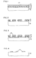
- Figure 1 is a cross-sectional view of an integrated circuit structure including a silicon wafer 10, a layer of polyimide 12, a layer of silicon dioxide 14, and a layer of photoresist 15.
- Substrate or wafer 10 will typically be a partially completed integrated circuit structure which may include active and.passive electronic components, layers of electrically conducting material, or other desired regions. As will be evident, the particular characteristics of substrate 10 are not critical to the invention, but simply provide an underlying structure which may be employed in the process of this invention.
- substrate 10 comprises a silicon substrate. This substrate is first coated with 5 to 6 nanometers of an adhesion promoter, such as EMDS manufactured by Petrarch Systems or VM-651 manufactured by DuPont. Either of these materials may be applied using a spinning operation, and will function to provide improved adhesion between subsequently deposited layers and the surface 11 of substrate 10.
- a suitable polyimide material 12 is then deposited to a thickness of 1.5 to 4.0 microns, also using a spinning operation.
- the polyimide material 12 comprises DuPont product DI-2555, or Ciba Geigy product XV-218-HP. After spinning the polyimide onto the wafer the material is cured in air by heating it slowly to 300°C and holding it at approximately that temperature for 30 minutes.
- silicon dioxide 14 Approximately 1300 Angstroms of silicon dioxide 14 are then deposited on the upper surface of polyimide 12 by using either vacuum deposition or plasma assisted chemical vapor deposition.
- the thickness of silicon dioxide 14 will be determined by the particular plasma etching step described below, however, thicknesses between 0.1 and 0.3 microns have been found suitable.
- photoresist 15 On the upper surface of silicon dioxide 14 a layer of positve photoresist between 0.5 and 1.0 microns thick is deposited using conventional techniques. The photoresist 15 is then cured by baking it to 90°C for approximately 6 minutes. In the preferred embodiment photoresist 15 is product AZ-1450J manufactured by Shipley Company, Inc-. and is approximately 0.5 microns thick.
- The. photoresist 15 is then exposed using conventional integrated circuit fabrication equipment, for example, a Mann stepper.
- the photoresist is developed and hardbaked for 30 minutes at temperature of 135°C.
- the silicon dioxide 14 is etched away where the photoresist has been removed. In the preferred embodiment this is achieved using carbon tetrafluoride plasma.
- Oxygen plasma is then used to etch the polyimide, and the structure is dipped in hydrochloric acid for 30 seconds to remove any residue. The appearance of the structure at this stage in the process is depicted in Figure 2.
- desired material 18 is then deposited across the structure.
- material 18 will comprise electrically conductive material used to form connections between various regions of the underlying substrate 10.
- the structure may be at a temperature up to or somewhat higher than 340°C during the deposition.
- metal 18 will be deposited both on the substrate 10 and on the silicon dioxide 14.
- the metal may be any desired thickness, however it must be sufficiently thin so as not to form a continuous coating across the surface of the structure, but rather only partially fill the openings as shown.
- polyimide 12 may be deposited thicker. Generally, the polyimide 12 will be formed to a thickness of 25% greater than the thickness of the desired metal 18.
- the metal must be deposited approximately normally to the upper surface 11 of wafer 10. In this manner the discontinuities between the various regions of.metal 18 on the polyimide 12 and the metal 18 on the substrate 10 are created.
- the structure is then heated to a temperature of 450-490°C in dry nitrogen for about 1 hour.
- This heat treatment is for the purpose of breaking the polymer bonds that exist between molecules of the adhesive layer, and also the bonds between the adhesive layer and the polyimide material.
- a partial hydrogen content may be used without interfering with the bond-breaking process, and, in addition, will give the hydrogen anneal at 450-490°C that is a normal step in subsequent processing of deposited metal contact structures.
- the lift-off structure comprising polyimide 12, silicon dioxide 14 and the undesired metal 18 deposited on silicon dioxide 14, is then removed. This may be achieved using either of two processes. In a first process the structure is placed in boiling distilled water with a wetting agent for approximately 30 minutes. It is then cleaned ultrasonically in methlyene chloride for 10 minutes. The cycle of boiling and ultrasonic treatment is repeated as many times as necessary to remove the lift-off material. The resulting structure is shown in Figure 4.
- a second technique for removing the lift-off material when ⁇ MDS has been used is to place the structure in boiling distilled water and then in a mixture of ethylene diamene and hydrazine (64% water) with a volume ratio of 60/40 at 30°C.
- the solution may be agitated ultrasonically. Complete delamination of the polyimide is observed in about 30 seconds to 10 minutes, yet metal 18 will remaine un- attacked for at least 15 minutes.
- the ethylene diamene is available from Aldrich Company in Milwaukee, Wisconsin, while the hydrazine is available from Matheson Coleman and Bell in Norwood, Ohio. If the adhesive agent VM-651 has been used, instead of EMS, the solution is heated to a temperature of 70°C and 30 minutes are required for removal of the lift-off material.
Abstract
Description
- This invention relates to the fabrication of integrated circuit structures, and in particular, to the fabrication of metal conducting lines on the surface of such structures using lift-off techniques, and the subsequent removal of the lift-off materials.
- Lift-off techniques for forming desired regions of material on the surface of integrated circuit structures are generally known. A survey of various lift-off processes is presented in "Lift-Off Techniques for Fine-Line Metal Patterning," by J. Frary and P. Seese, Semiconductor International, December 1981, pages 70-89.
- In conventional integrated circuit fabrication technology, patterns of desired material are formed on the surface of an integrated circuit structure using etching techniques. Such processes suffer from a number of disadvantages which restrict their application, particularly in the fabrication of integrated circuit structures having exceptionally small regions. For example, to insure complete etch removal of deposited material, the pattern must always be at least slightly over-etched, leading to diminished line widths for a particular line spacing. Although this problem may be lessened by using plasma or reactive ion etching, these processes in turn create chemical contamination problems which must also be solved.
- The use of lift-off processes circumvents many of these disadvantages. For example, because the integrated circuit structure itself is not subjected to plasma or reactive ion etching, radiation damage to active devices is minimized. Furthermore, lift-off processing is usable over a wide range of temperatures for patterning many materials commonly used in the fabrication of integrated circuits.
- Because the lift-off material, typically a polyimide, must be firmly anchored to the underlying integrated circuit to allow accurate patterning of the lift-off material itself, it is often difficult to completely remove the lift-off material from the surface of the circuit at the end of a process sequence. This difficulty is further increased when adhesives are used for attaching the lift-off material to the surface of the circuit, and when the polyimide itself is generally insoluble. Incomplete removal of the lift-off material generally results in lower yields by creating short circuits or obscuring portions of the surface of the integrated circuit structure from subsequent process operations.
- It is a general object of the present invention to provide an improved lift-off process.
- This and other objects are attained, in accordance with one aspect of the invention, by a process for removing polyimide regions adhered to semiconductor structures comprising heating the structure and the polyimide regions to between 450° and 490°C; immersing the structure in a solution of one of methylene chloride and ethylene diamene/hydrazine; and ultrasonerating the solution and the semiconductor structure.
-
- Figure 1 is a cross-sectional view of an integrated circuit structure before patterning.
- Figure 2 is a subsequent cross-sectional view after patterning.
- Figure 3 is a subsequent cross-sectional view after forming desired metal connections.
- Figure 4 is a subsequent cross-sectional view after adhesion bond-breaking of the lift-off material.
- Figure 1 is a cross-sectional view of an integrated circuit structure including a
silicon wafer 10, a layer ofpolyimide 12, a layer ofsilicon dioxide 14, and a layer ofphotoresist 15. Substrate orwafer 10 will typically be a partially completed integrated circuit structure which may include active and.passive electronic components, layers of electrically conducting material, or other desired regions. As will be evident, the particular characteristics ofsubstrate 10 are not critical to the invention, but simply provide an underlying structure which may be employed in the process of this invention. - In the
preferred embodiment substrate 10 comprises a silicon substrate. This substrate is first coated with 5 to 6 nanometers of an adhesion promoter, such as EMDS manufactured by Petrarch Systems or VM-651 manufactured by DuPont. Either of these materials may be applied using a spinning operation, and will function to provide improved adhesion between subsequently deposited layers and the surface 11 ofsubstrate 10. Asuitable polyimide material 12 is then deposited to a thickness of 1.5 to 4.0 microns, also using a spinning operation. In the preferred embodiment thepolyimide material 12 comprises DuPont product DI-2555, or Ciba Geigy product XV-218-HP. After spinning the polyimide onto the wafer the material is cured in air by heating it slowly to 300°C and holding it at approximately that temperature for 30 minutes. - Approximately 1300 Angstroms of
silicon dioxide 14 are then deposited on the upper surface ofpolyimide 12 by using either vacuum deposition or plasma assisted chemical vapor deposition. The thickness ofsilicon dioxide 14 will be determined by the particular plasma etching step described below, however, thicknesses between 0.1 and 0.3 microns have been found suitable. - On the upper surface of silicon dioxide 14 a layer of positve photoresist between 0.5 and 1.0 microns thick is deposited using conventional techniques. The
photoresist 15 is then cured by baking it to 90°C for approximately 6 minutes. In the preferredembodiment photoresist 15 is product AZ-1450J manufactured by Shipley Company, Inc-. and is approximately 0.5 microns thick. - The. photoresist 15 is then exposed using conventional integrated circuit fabrication equipment, for example, a Mann stepper. The photoresist is developed and hardbaked for 30 minutes at temperature of 135°C. Using well-known plasma or reactive ion etching apparatus, the
silicon dioxide 14 is etched away where the photoresist has been removed. In the preferred embodiment this is achieved using carbon tetrafluoride plasma. Oxygen plasma is then used to etch the polyimide, and the structure is dipped in hydrochloric acid for 30 seconds to remove any residue. The appearance of the structure at this stage in the process is depicted in Figure 2. - As shown by Figure 3 desired
material 18 is then deposited across the structure. Typicallymaterial 18 will comprise electrically conductive material used to form connections between various regions of theunderlying substrate 10. The structure may be at a temperature up to or somewhat higher than 340°C during the deposition. As shown by Figure 3metal 18 will be deposited both on thesubstrate 10 and on thesilicon dioxide 14. The metal may be any desired thickness, however it must be sufficiently thin so as not to form a continuous coating across the surface of the structure, but rather only partially fill the openings as shown. Of course ifthicker metal 18 is desired,polyimide 12 may be deposited thicker. Generally, thepolyimide 12 will be formed to a thickness of 25% greater than the thickness of the desiredmetal 18. To form the metal in the manner depicted in Figure 3, the metal must be deposited approximately normally to the upper surface 11 ofwafer 10. In this manner the discontinuities between the various regions of.metal 18 on thepolyimide 12 and themetal 18 on thesubstrate 10 are created. - The structure is then heated to a temperature of 450-490°C in dry nitrogen for about 1 hour. This heat treatment is for the purpose of breaking the polymer bonds that exist between molecules of the adhesive layer, and also the bonds between the adhesive layer and the polyimide material.. It is to be noted that a partial hydrogen content may be used without interfering with the bond-breaking process, and, in addition, will give the hydrogen anneal at 450-490°C that is a normal step in subsequent processing of deposited metal contact structures.
- The lift-off
structure comprising polyimide 12,silicon dioxide 14 and theundesired metal 18 deposited onsilicon dioxide 14, is then removed. This may be achieved using either of two processes. In a first process the structure is placed in boiling distilled water with a wetting agent for approximately 30 minutes. It is then cleaned ultrasonically in methlyene chloride for 10 minutes. The cycle of boiling and ultrasonic treatment is repeated as many times as necessary to remove the lift-off material. The resulting structure is shown in Figure 4. - A second technique for removing the lift-off material when ΞMDS has been used is to place the structure in boiling distilled water and then in a mixture of ethylene diamene and hydrazine (64% water) with a volume ratio of 60/40 at 30°C. The solution may be agitated ultrasonically. Complete delamination of the polyimide is observed in about 30 seconds to 10 minutes, yet
metal 18 will remaine un- attacked for at least 15 minutes. The ethylene diamene is available from Aldrich Company in Milwaukee, Wisconsin, while the hydrazine is available from Matheson Coleman and Bell in Norwood, Ohio. If the adhesive agent VM-651 has been used, instead of EMS, the solution is heated to a temperature of 70°C and 30 minutes are required for removal of the lift-off material. - The foregoing description is intended to describe the preferred embodiments of the invention. It will be apparent, however, that numerous variations may be made in the process without departing from the scope of the invention as defined in the appended claims.
Claims (7)
Applications Claiming Priority (2)
| Application Number | Priority Date | Filing Date | Title |
|---|---|---|---|
| US06/404,108 US4428796A (en) | 1982-08-02 | 1982-08-02 | Adhesion bond-breaking of lift-off regions on semiconductor structures |
| US404108 | 1982-08-02 |
Publications (3)
| Publication Number | Publication Date |
|---|---|
| EP0102281A2 true EP0102281A2 (en) | 1984-03-07 |
| EP0102281A3 EP0102281A3 (en) | 1986-03-26 |
| EP0102281B1 EP0102281B1 (en) | 1989-02-01 |
Family
ID=23598195
Family Applications (1)
| Application Number | Title | Priority Date | Filing Date |
|---|---|---|---|
| EP83401592A Expired EP0102281B1 (en) | 1982-08-02 | 1983-08-01 | Adhesion bond-breaking of lift-off regions on semiconductor structures |
Country Status (5)
| Country | Link |
|---|---|
| US (1) | US4428796A (en) |
| EP (1) | EP0102281B1 (en) |
| JP (1) | JPS5944830A (en) |
| CA (1) | CA1192480A (en) |
| DE (1) | DE3379133D1 (en) |
Cited By (6)
| Publication number | Priority date | Publication date | Assignee | Title |
|---|---|---|---|---|
| EP0134938A2 (en) * | 1983-07-26 | 1985-03-27 | International Business Machines Corporation | Dry process for forming metal patterns on a surface |
| EP0149060A2 (en) * | 1983-11-30 | 1985-07-24 | International Business Machines Corporation | Lift-off process for forming metal patterns |
| EP0199300A2 (en) * | 1985-04-19 | 1986-10-29 | Matsushita Electronics Corporation | Method for making a patterned metal layer |
| EP0200082A2 (en) * | 1985-04-30 | 1986-11-05 | International Business Machines Corporation | Barrierless high-temperature Lift-off process for forming a patterned interconnection layer |
| EP0311817A2 (en) * | 1987-10-15 | 1989-04-19 | Fujitsu Limited | Method for removing an ion-implanted organic resin layer during fabrication of semiconductor devices |
| EP0511691A2 (en) * | 1988-07-13 | 1992-11-04 | International Business Machines Corporation | Wet etching of chemically cured polyimide |
Families Citing this family (19)
| Publication number | Priority date | Publication date | Assignee | Title |
|---|---|---|---|---|
| DE3604368A1 (en) * | 1985-02-13 | 1986-08-14 | Sharp K.K., Osaka | METHOD FOR PRODUCING A THIN FILM TRANSISTOR |
| US4744863A (en) * | 1985-04-26 | 1988-05-17 | Wisconsin Alumni Research Foundation | Sealed cavity semiconductor pressure transducers and method of producing the same |
| US4853669A (en) * | 1985-04-26 | 1989-08-01 | Wisconsin Alumni Research Foundation | Sealed cavity semiconductor pressure transducers and method of producing the same |
| US4715109A (en) * | 1985-06-12 | 1987-12-29 | Texas Instruments Incorporated | Method of forming a high density vertical stud titanium silicide for reachup contact applications |
| US4886573A (en) * | 1986-08-27 | 1989-12-12 | Hitachi, Ltd. | Process for forming wiring on substrate |
| US4861425A (en) * | 1988-08-22 | 1989-08-29 | International Business Machines Corporation | Lift-off process for terminal metals |
| US6989228B2 (en) | 1989-02-27 | 2006-01-24 | Hitachi, Ltd | Method and apparatus for processing samples |
| US5868854A (en) * | 1989-02-27 | 1999-02-09 | Hitachi, Ltd. | Method and apparatus for processing samples |
| US5232872A (en) * | 1989-05-09 | 1993-08-03 | Fujitsu Limited | Method for manufacturing semiconductor device |
| US5006488A (en) * | 1989-10-06 | 1991-04-09 | International Business Machines Corporation | High temperature lift-off process |
| US5140396A (en) * | 1990-10-10 | 1992-08-18 | Polaroid Corporation | Filter and solid state imager incorporating this filter |
| US5059500A (en) * | 1990-10-10 | 1991-10-22 | Polaroid Corporation | Process for forming a color filter |
| US5382315A (en) * | 1991-02-11 | 1995-01-17 | Microelectronics And Computer Technology Corporation | Method of forming etch mask using particle beam deposition |
| US5244538A (en) * | 1991-07-26 | 1993-09-14 | Microelectronics And Computer Technology Corporation | Method of patterning metal on a substrate using direct-write deposition of a mask |
| US5350487A (en) * | 1993-05-03 | 1994-09-27 | Ameen Thomas J | Method of etching polyimide |
| US5925260A (en) * | 1997-01-02 | 1999-07-20 | Micron Technology, Inc. | Removal of polyimide from dies and wafers |
| DE19717363C2 (en) * | 1997-04-24 | 2001-09-06 | Siemens Ag | Manufacturing process for a platinum metal structure using a lift-off process and use of the manufacturing process |
| US6656313B2 (en) * | 2001-06-11 | 2003-12-02 | International Business Machines Corporation | Structure and method for improved adhesion between two polymer films |
| US20060108322A1 (en) * | 2004-11-19 | 2006-05-25 | Wei Wu | Lift-off material |
Citations (5)
| Publication number | Priority date | Publication date | Assignee | Title |
|---|---|---|---|---|
| US3988256A (en) * | 1974-04-03 | 1976-10-26 | Allied Chemical Corporation | Photoresist stripper rinse |
| FR2376447A1 (en) * | 1976-12-30 | 1978-07-28 | Ibm | PROCESS FOR FORMING A THIN FILM CONFIGURATION ON A SUBSTRATE USING A POLYIMIDE MASK |
| US4218283A (en) * | 1974-08-23 | 1980-08-19 | Hitachi, Ltd. | Method for fabricating semiconductor device and etchant for polymer resin |
| EP0025261A1 (en) * | 1979-07-31 | 1981-03-18 | Fujitsu Limited | A method of manufacturing a semiconductor device |
| EP0100736A2 (en) * | 1982-08-02 | 1984-02-15 | Fairchild Semiconductor Corporation | Structure and process for lift-off wafer processing |
Family Cites Families (2)
| Publication number | Priority date | Publication date | Assignee | Title |
|---|---|---|---|---|
| JPS5127464A (en) * | 1974-08-23 | 1976-03-08 | Hitachi Ltd | HORIIMIDOKEIJUSHIMAKUNO SENTAKUTEKIETSUCHINGUHOHO |
| JPS5874041A (en) * | 1981-10-29 | 1983-05-04 | Hitachi Chem Co Ltd | Etchant for polyimide resin |
-
1982
- 1982-08-02 US US06/404,108 patent/US4428796A/en not_active Expired - Lifetime
-
1983
- 1983-07-29 CA CA000433552A patent/CA1192480A/en not_active Expired
- 1983-08-01 JP JP58139525A patent/JPS5944830A/en active Granted
- 1983-08-01 DE DE8383401592T patent/DE3379133D1/en not_active Expired
- 1983-08-01 EP EP83401592A patent/EP0102281B1/en not_active Expired
Patent Citations (5)
| Publication number | Priority date | Publication date | Assignee | Title |
|---|---|---|---|---|
| US3988256A (en) * | 1974-04-03 | 1976-10-26 | Allied Chemical Corporation | Photoresist stripper rinse |
| US4218283A (en) * | 1974-08-23 | 1980-08-19 | Hitachi, Ltd. | Method for fabricating semiconductor device and etchant for polymer resin |
| FR2376447A1 (en) * | 1976-12-30 | 1978-07-28 | Ibm | PROCESS FOR FORMING A THIN FILM CONFIGURATION ON A SUBSTRATE USING A POLYIMIDE MASK |
| EP0025261A1 (en) * | 1979-07-31 | 1981-03-18 | Fujitsu Limited | A method of manufacturing a semiconductor device |
| EP0100736A2 (en) * | 1982-08-02 | 1984-02-15 | Fairchild Semiconductor Corporation | Structure and process for lift-off wafer processing |
Non-Patent Citations (2)
| Title |
|---|
| IBM TECHNICAL DISCLOSURE BULLETIN, vol. 25, no. 2, July 1982, pages 532-533, New York, US; N.R.POULIN: "Double step lift-off process for chip pad metallurgy" * |
| IEEE TRANSACTIONS ON ELECTRON DEVICES, vol. ED-28, no. 5, May 1981, pages 552-556, IEEE, New York, US; YOSHIO HOMMA et al.: "Polyimide liftoff technology for high-density LSI metallization" * |
Cited By (12)
| Publication number | Priority date | Publication date | Assignee | Title |
|---|---|---|---|---|
| EP0134938A2 (en) * | 1983-07-26 | 1985-03-27 | International Business Machines Corporation | Dry process for forming metal patterns on a surface |
| EP0134938A3 (en) * | 1983-07-26 | 1985-08-14 | International Business Machines Corporation | Dry process for forming metal patterns on a surface |
| EP0149060A2 (en) * | 1983-11-30 | 1985-07-24 | International Business Machines Corporation | Lift-off process for forming metal patterns |
| EP0149060A3 (en) * | 1983-11-30 | 1985-07-31 | International Business Machines Corporation | Lift-off process for forming metal patterns |
| EP0199300A2 (en) * | 1985-04-19 | 1986-10-29 | Matsushita Electronics Corporation | Method for making a patterned metal layer |
| EP0199300A3 (en) * | 1985-04-19 | 1988-11-23 | Matsushita Electronics Corporation | Method for making a mask having perpendicular side wall and method for making a patterned metal layer by using the former method |
| EP0200082A2 (en) * | 1985-04-30 | 1986-11-05 | International Business Machines Corporation | Barrierless high-temperature Lift-off process for forming a patterned interconnection layer |
| EP0200082A3 (en) * | 1985-04-30 | 1988-11-17 | International Business Machines Corporation | Barrierless high-temperature lift-off process for forming a patterned interconnection layer |
| EP0311817A2 (en) * | 1987-10-15 | 1989-04-19 | Fujitsu Limited | Method for removing an ion-implanted organic resin layer during fabrication of semiconductor devices |
| EP0311817A3 (en) * | 1987-10-15 | 1990-06-13 | Fujitsu Limited | Method for removing an ion-implanted organic resin layer during fabrication of semiconductor devices |
| EP0511691A2 (en) * | 1988-07-13 | 1992-11-04 | International Business Machines Corporation | Wet etching of chemically cured polyimide |
| EP0511691A3 (en) * | 1988-07-13 | 1993-03-03 | International Business Machines Corporation | Wet etching of cured polyimide |
Also Published As
| Publication number | Publication date |
|---|---|
| US4428796A (en) | 1984-01-31 |
| EP0102281A3 (en) | 1986-03-26 |
| EP0102281B1 (en) | 1989-02-01 |
| JPH0345895B2 (en) | 1991-07-12 |
| JPS5944830A (en) | 1984-03-13 |
| DE3379133D1 (en) | 1989-03-09 |
| CA1192480A (en) | 1985-08-27 |
Similar Documents
| Publication | Publication Date | Title |
|---|---|---|
| US4428796A (en) | Adhesion bond-breaking of lift-off regions on semiconductor structures | |
| US4440804A (en) | Lift-off process for fabricating self-aligned contacts | |
| US4357203A (en) | Plasma etching of polyimide | |
| EP0200082B1 (en) | Barrierless high-temperature lift-off process for forming a patterned interconnection layer | |
| US4152195A (en) | Method of improving the adherence of metallic conductive lines on polyimide layers | |
| EP0046525B1 (en) | Planar multi-level metal-insulator structure comprising a substrate, a conductive interconnection pattern and a superposed conductive structure and a method to form such a structure | |
| JP3135930B2 (en) | Thin film electrical equipment | |
| US3846166A (en) | Method of producing multilayer wiring structure of integrated circuit | |
| US20010025725A1 (en) | Electrically Conductive Apparatuses | |
| WO1997022989A1 (en) | Process for single mask c4 solder bump fabrication | |
| US4631806A (en) | Method of producing integrated circuit structures | |
| JP2932940B2 (en) | Method of manufacturing semiconductor device having thin film resistor | |
| US3767490A (en) | Process for etching organic coating layers | |
| US4089766A (en) | Method of passivating and planarizing a metallization pattern | |
| US6376155B2 (en) | Patterning method in semiconductor device fabricating process | |
| CN107230645A (en) | Semiconductor structure and its manufacture method | |
| US4081315A (en) | Cermet etch technique | |
| JP2509175B2 (en) | Manufacturing method of wiring structure | |
| US6504248B2 (en) | Thin film circuit substrate and manufacturing method therefor | |
| JP2842405B2 (en) | Method for manufacturing semiconductor device | |
| JPH03198342A (en) | Manufacture of semiconductor device | |
| JPH0611042B2 (en) | Method for manufacturing semiconductor device | |
| JP3532972B2 (en) | Method for manufacturing compound semiconductor device | |
| JP2000174127A (en) | Manufacture of semiconductor device | |
| JPH04132221A (en) | Manufacture of semiconductor integrated circuit |
Legal Events
| Date | Code | Title | Description |
|---|---|---|---|
| PUAI | Public reference made under article 153(3) epc to a published international application that has entered the european phase |
Free format text: ORIGINAL CODE: 0009012 |
|
| AK | Designated contracting states |
Designated state(s): DE FR GB IT NL |
|
| PUAL | Search report despatched |
Free format text: ORIGINAL CODE: 0009013 |
|
| AK | Designated contracting states |
Kind code of ref document: A3 Designated state(s): DE FR GB IT NL |
|
| 17P | Request for examination filed |
Effective date: 19860901 |
|
| 17Q | First examination report despatched |
Effective date: 19880330 |
|
| RAP1 | Party data changed (applicant data changed or rights of an application transferred) |
Owner name: FAIRCHILD SEMICONDUCTOR CORPORATION |
|
| GRAA | (expected) grant |
Free format text: ORIGINAL CODE: 0009210 |
|
| AK | Designated contracting states |
Kind code of ref document: B1 Designated state(s): DE FR GB IT NL |
|
| REF | Corresponds to: |
Ref document number: 3379133 Country of ref document: DE Date of ref document: 19890309 |
|
| ET | Fr: translation filed | ||
| ITF | It: translation for a ep patent filed |
Owner name: STUDIO TORTA SOCIETA' SEMPLICE |
|
| PLBE | No opposition filed within time limit |
Free format text: ORIGINAL CODE: 0009261 |
|
| STAA | Information on the status of an ep patent application or granted ep patent |
Free format text: STATUS: NO OPPOSITION FILED WITHIN TIME LIMIT |
|
| 26N | No opposition filed | ||
| ITTA | It: last paid annual fee | ||
| PGFP | Annual fee paid to national office [announced via postgrant information from national office to epo] |
Ref country code: GB Payment date: 19940711 Year of fee payment: 12 |
|
| PGFP | Annual fee paid to national office [announced via postgrant information from national office to epo] |
Ref country code: FR Payment date: 19940812 Year of fee payment: 12 |
|
| PGFP | Annual fee paid to national office [announced via postgrant information from national office to epo] |
Ref country code: NL Payment date: 19940831 Year of fee payment: 12 |
|
| PG25 | Lapsed in a contracting state [announced via postgrant information from national office to epo] |
Ref country code: GB Effective date: 19950801 |
|
| PG25 | Lapsed in a contracting state [announced via postgrant information from national office to epo] |
Ref country code: NL Effective date: 19960301 |
|
| GBPC | Gb: european patent ceased through non-payment of renewal fee |
Effective date: 19950801 |
|
| PG25 | Lapsed in a contracting state [announced via postgrant information from national office to epo] |
Ref country code: FR Effective date: 19960430 |
|
| NLV4 | Nl: lapsed or anulled due to non-payment of the annual fee |
Effective date: 19960301 |
|
| REG | Reference to a national code |
Ref country code: FR Ref legal event code: ST |
|
| PGFP | Annual fee paid to national office [announced via postgrant information from national office to epo] |
Ref country code: DE Payment date: 20020830 Year of fee payment: 20 |