EP0099787A1 - Procédé d'optimisation du dopage dans un transistor MOS - Google Patents
Procédé d'optimisation du dopage dans un transistor MOS Download PDFInfo
- Publication number
- EP0099787A1 EP0099787A1 EP83401331A EP83401331A EP0099787A1 EP 0099787 A1 EP0099787 A1 EP 0099787A1 EP 83401331 A EP83401331 A EP 83401331A EP 83401331 A EP83401331 A EP 83401331A EP 0099787 A1 EP0099787 A1 EP 0099787A1
- Authority
- EP
- European Patent Office
- Prior art keywords
- ions
- substrate
- type
- doping
- transistor
- Prior art date
- Legal status (The legal status is an assumption and is not a legal conclusion. Google has not performed a legal analysis and makes no representation as to the accuracy of the status listed.)
- Withdrawn
Links
Images
Classifications
-
- H10P30/21—
-
- H—ELECTRICITY
- H10—SEMICONDUCTOR DEVICES; ELECTRIC SOLID-STATE DEVICES NOT OTHERWISE PROVIDED FOR
- H10D—INORGANIC ELECTRIC SEMICONDUCTOR DEVICES
- H10D30/00—Field-effect transistors [FET]
- H10D30/01—Manufacture or treatment
- H10D30/021—Manufacture or treatment of FETs having insulated gates [IGFET]
- H10D30/0223—Manufacture or treatment of FETs having insulated gates [IGFET] having source and drain regions or source and drain extensions self-aligned to sides of the gate
- H10D30/0227—Manufacture or treatment of FETs having insulated gates [IGFET] having source and drain regions or source and drain extensions self-aligned to sides of the gate having both lightly-doped source and drain extensions and source and drain regions self-aligned to the sides of the gate, e.g. lightly-doped drain [LDD] MOSFET or double-diffused drain [DDD] MOSFET
-
- H—ELECTRICITY
- H10—SEMICONDUCTOR DEVICES; ELECTRIC SOLID-STATE DEVICES NOT OTHERWISE PROVIDED FOR
- H10D—INORGANIC ELECTRIC SEMICONDUCTOR DEVICES
- H10D62/00—Semiconductor bodies, or regions thereof, of devices having potential barriers
- H10D62/10—Shapes, relative sizes or dispositions of the regions of the semiconductor bodies; Shapes of the semiconductor bodies
- H10D62/13—Semiconductor regions connected to electrodes carrying current to be rectified, amplified or switched, e.g. source or drain regions
- H10D62/149—Source or drain regions of field-effect devices
- H10D62/151—Source or drain regions of field-effect devices of IGFETs
-
- H—ELECTRICITY
- H10—SEMICONDUCTOR DEVICES; ELECTRIC SOLID-STATE DEVICES NOT OTHERWISE PROVIDED FOR
- H10D—INORGANIC ELECTRIC SEMICONDUCTOR DEVICES
- H10D62/00—Semiconductor bodies, or regions thereof, of devices having potential barriers
- H10D62/10—Shapes, relative sizes or dispositions of the regions of the semiconductor bodies; Shapes of the semiconductor bodies
- H10D62/17—Semiconductor regions connected to electrodes not carrying current to be rectified, amplified or switched, e.g. channel regions
- H10D62/351—Substrate regions of field-effect devices
- H10D62/357—Substrate regions of field-effect devices of FETs
- H10D62/364—Substrate regions of field-effect devices of FETs of IGFETs
- H10D62/371—Inactive supplementary semiconductor regions, e.g. for preventing punch-through, improving capacity effect or leakage current
-
- H10P30/204—
Definitions
- one of the possible methods would consist in increasing the doping of the substrate in the region thereof situated only under the gate of the transistor, so as not to increase the doping in the regions of the substrate located below the source and the drain of this transistor.
- the subject of the present invention is precisely a method for optimizing doping in a MOS transistor making it possible to obtain such a doping profile.
- this doping profile is obtained by compensating, at the source and the drain of the MOS transistor, the doping of the substrate under the channel of this transistor.
- the subject of the invention is a method for optimizing doping in a MOS transistor, this transistor being produced on a doped silicon substrate, having a doping profile defined by an implantation of ions belonging to a first type of ions giving a doping of the same type as that of the substrate, a source and a drain defined, in said substrate, by an implantation of ions belonging to a second type of ions giving a doping different from that of the substrate, and a gate, characterized in that one or more implantations of ions belonging to the second type of ions are carried out, under the source and the drain of the transistor, at doses and energies such that they compensate for the doping of the substrate without inverting the type, the gate of the transistor serving as a mask for this implantation, and in that the substrate is subjected to annealing.
- the fact of using the gate of the transistor as a mask for the implantation of ions under the source and the drain of the transistor makes it possible to obtain self-aligned compensation regions with respect to the gate of the transistor.
- the substrate is subjected to a transient annealing, this annealing being carried out either by means of a laser beam, or by means of an electron beam, or else by means of radiant heating by lamps or heating resistors.
- the substrate being made of P-type silicon
- the ions belonging to the first type of ions are boron ions and the ions belonging to the second type of ions are phosphorus or arsenic ions.
- the substrate being made of type N silicon
- the ions belonging to the first type of ions are phosphorus or arsenic ions and the ions belonging to the second type of ions are ions of boron.
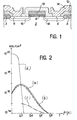
- FIG. 1 there is shown, in cross section, the structure of an MOS transistor.
- This MOS transistor produced on a doped semiconductor substrate 2, in an opening of the field oxide 3, conventionally comprises two lateral regions 4 and 6, corresponding respectively to the source and to the drain of this transistor, and a oxide layer 8, covering the central region of the substrate 2, surmounted by a conductive layer 10.
- the conductive layer 10 corresponds to the gate of the transistor and the oxide layer 8 to the gate oxide.
- the whole of the MOS transistor is covered with an oxide layer 12, etched so as to define the electrical contact holes of the transistor, this oxide layer 12 itself being covered with a conductive layer 14, etched with way to define the electrical connections.
- this MOS transistor is done, first of all, by producing the field oxide 3 and the gate oxide 8, then by implanting boron ions making it possible to define the doping under the channel of the transistor.
- This ion implantation is for example carried out at a dose of 10 12 atoms / cm2 and at an energy of 50 KeV, then at a dose of 4.10 11 atoms / cm2 and at an energy of 140 keV.
- the gate 10 of the transistor is produced, generally in a layer of doped polycrystalline silicon, then the source 4 and drain 6 of this transistor.
- the source and the drain of this transistor are obtained by implanting phosphorus or arsenic ions, this implantation being carried out using the gate of the transistor as a mask at said implantation. This implantation is for example carried out for arsenic ions at a dose of 5.10 15 atoms / cm 2 and at an energy of 100 keV.
- the oxide layer 12 is deposited over the entire substrate 2, which is etched so as to make the electrical contact holes of the transistor, then this oxide layer 12 is covered with a layer conductive 14, generally made of aluminum, which is etched appropriately to make the electrical connections of the transistor.
- one or more implantations of phosphorus or arsenic ions are carried out, under the source 4 and under the drain 6 of the transistor, optionally followed by a boron implantation, the number of implantations being a function of the quantity and of the profile of boron ions used for the definition of the doping under the channel as well as of the profile of this doping.
- This implantation which is carried out before depositing the oxide layer 12 on the substrate, makes it possible to obtain two lateral regions 16 and 18 located respectively under the source 4 and under the drain 6 of the transistor.
- this implantation will be carried out using the gate of the transistor as a mask at said implantation.
- the substrate 2 is subjected to an annealing.
- a transient annealing is used which makes it possible to avoid or minimize the diffusion of the ions implanted under the source and the drain of the transistor.
- This annealing can be carried out either by means of a laser beam, or by means of an electron beam, or by means of radiative heating by lamps or heating resistors.
- FIG. 2 shows curves giving the quantity of ions implanted per cm 3 , for the different dopings, carried out during the manufacture of the MOS transistor, as a function of the penetration depth P of the ions in the substrate.
- the doping profile a corresponds to the implantation defining the channel of the transistor, this implantation being made, in the present example, with boron ions.
- the doping profile b corresponds to the implantation making it possible to compensate for the previous implantation, in accordance with the invention. This implementation is carried out in the pre feels example, with phosphorus ions.
- the doping profile c corresponds to the result of the curve a and of the curve b, that is to say to the profile of the doping resulting from the two previous implantations.
- the doping profile d corresponds to the implantation defining the source and the drain of the transistor, this implantation being carried out in the present example with phosphorus ions.
- the doping method makes it possible to reduce the stray capacitances between the source, the drain and the substrate of the transistor.
Landscapes
- Metal-Oxide And Bipolar Metal-Oxide Semiconductor Integrated Circuits (AREA)
- Insulated Gate Type Field-Effect Transistor (AREA)
- Bipolar Transistors (AREA)
Applications Claiming Priority (2)
| Application Number | Priority Date | Filing Date | Title |
|---|---|---|---|
| FR8211571 | 1982-07-01 | ||
| FR8211571A FR2529715A1 (fr) | 1982-07-01 | 1982-07-01 | Procede d'optimisation du dopage dans un transistor mos |
Publications (1)
| Publication Number | Publication Date |
|---|---|
| EP0099787A1 true EP0099787A1 (fr) | 1984-02-01 |
Family
ID=9275586
Family Applications (1)
| Application Number | Title | Priority Date | Filing Date |
|---|---|---|---|
| EP83401331A Withdrawn EP0099787A1 (fr) | 1982-07-01 | 1983-06-28 | Procédé d'optimisation du dopage dans un transistor MOS |
Country Status (3)
| Country | Link |
|---|---|
| EP (1) | EP0099787A1 (enExample) |
| JP (1) | JPS5921068A (enExample) |
| FR (1) | FR2529715A1 (enExample) |
Cited By (4)
| Publication number | Priority date | Publication date | Assignee | Title |
|---|---|---|---|---|
| EP0343360A3 (en) * | 1988-05-20 | 1990-02-21 | International Business Machines Corporation | Method for fabricating shallow junctions |
| EP0255882A3 (de) * | 1986-08-07 | 1990-05-30 | Siemens Aktiengesellschaft | npn-Bipolartransistor mit extrem flachen Emitter/Basis-Strukturen und Verfahren zu seiner Herstellung |
| EP0359530A3 (en) * | 1988-09-15 | 1991-01-02 | Advanced Micro Devices, Inc. | Capacitive reduction of junctions in a semiconductor device |
| WO1990010309A3 (en) * | 1989-03-02 | 1991-01-24 | Thunderbird Tech Inc | Fermi threshold field effect transistor |
Citations (1)
| Publication number | Priority date | Publication date | Assignee | Title |
|---|---|---|---|---|
| FR2337428A1 (fr) * | 1975-12-31 | 1977-07-29 | Ibm | Transistor a effet de champ a canal composite et procede de fabrication |
-
1982
- 1982-07-01 FR FR8211571A patent/FR2529715A1/fr active Granted
-
1983
- 1983-06-28 EP EP83401331A patent/EP0099787A1/fr not_active Withdrawn
- 1983-07-01 JP JP58118387A patent/JPS5921068A/ja active Pending
Patent Citations (1)
| Publication number | Priority date | Publication date | Assignee | Title |
|---|---|---|---|---|
| FR2337428A1 (fr) * | 1975-12-31 | 1977-07-29 | Ibm | Transistor a effet de champ a canal composite et procede de fabrication |
Non-Patent Citations (4)
| Title |
|---|
| APPLIED PHYSICS LETTERS, vol. 35, no. 8, octobre 1979, pages 621-623, New York, USA * |
| IBM TECHNICAL DISCLOSURE BULLETIN, vol. 17, no. 4, septembre 1974, pages 1208-1209, New York, USA * |
| IEEE ELECTRON DEVICES, vol. ED-27, no. 8, août 1980, pages 1559-1565, New York, USA * |
| IEEE JOURNAL OF SOLID-STATE CIRCUITS, vol. SC-14, no. 3, juin 1979, pages 651-653, New York, USA * |
Cited By (4)
| Publication number | Priority date | Publication date | Assignee | Title |
|---|---|---|---|---|
| EP0255882A3 (de) * | 1986-08-07 | 1990-05-30 | Siemens Aktiengesellschaft | npn-Bipolartransistor mit extrem flachen Emitter/Basis-Strukturen und Verfahren zu seiner Herstellung |
| EP0343360A3 (en) * | 1988-05-20 | 1990-02-21 | International Business Machines Corporation | Method for fabricating shallow junctions |
| EP0359530A3 (en) * | 1988-09-15 | 1991-01-02 | Advanced Micro Devices, Inc. | Capacitive reduction of junctions in a semiconductor device |
| WO1990010309A3 (en) * | 1989-03-02 | 1991-01-24 | Thunderbird Tech Inc | Fermi threshold field effect transistor |
Also Published As
| Publication number | Publication date |
|---|---|
| FR2529715B1 (enExample) | 1984-12-21 |
| JPS5921068A (ja) | 1984-02-02 |
| FR2529715A1 (fr) | 1984-01-06 |
Similar Documents
| Publication | Publication Date | Title |
|---|---|---|
| JP2578204B2 (ja) | 半導体デバイスの製造方法 | |
| US4315781A (en) | Method of controlling MOSFET threshold voltage with self-aligned channel stop | |
| US5793089A (en) | Graded MOS transistor junction formed by aligning a sequence of implants to a selectively removable polysilicon sidewall space and oxide thermally grown thereon | |
| CN100399576C (zh) | 于沟道区域中具有退化掺杂分布的半导体组件及用于制造该半导体组件的方法 | |
| CN1148791C (zh) | 具有可独立调节参数的晶体管的结构与工艺集成 | |
| US5895955A (en) | MOS transistor employing a removable, dual layer etch stop to protect implant regions from sidewall spacer overetch | |
| EP1266409A1 (fr) | Transistor mos a source et drain metalliques, et procede de fabrication d'un tel transistor | |
| EP0164281A1 (fr) | Procédé de fabrication d'une couche isolante enterrée dans un substrat semiconducteur, par implantation ionique | |
| US6514785B1 (en) | CMOS image sensor n-type pin-diode structure | |
| FR2663464A1 (fr) | Circuit integre en technologie silicium sur isolant comportant un transistor a effet de champ et son procede de fabrication. | |
| FR2647596A1 (fr) | Transistor a effet de champ a grille isolee et procede de fabrication | |
| FR2577348A1 (fr) | Procede de formation de regions de silicium isolees et de dispositifs a effet de champ sur un substrat de silicium | |
| FR2498812A1 (fr) | Structure de transistors dans un circuit integre et son procede de fabrication | |
| EP0172772A2 (fr) | Circuit intégré CMOS et procédé de fabrication de zones d'isolation électrique dans ce circuit intégré | |
| FR2481518A1 (fr) | Procede de realisation d'un dispositif semiconducteur comportant des transistors a effet de champ complementaires | |
| EP0203836A1 (fr) | Procédé de fabrication de transistors à effet de champ, et transistors bipolaires latéraux sur un même substrat | |
| EP0750339A1 (fr) | Procédé de fabrication de transistors | |
| EP0099787A1 (fr) | Procédé d'optimisation du dopage dans un transistor MOS | |
| TWI234849B (en) | Structure and method of controlling short-channel effect of very short channel MOSFET | |
| US6617214B2 (en) | Integrated circuit structure and method therefore | |
| US6096586A (en) | MOS device with self-compensating VaT -implants | |
| FR2742583A1 (fr) | Transistor a effet de champ a grille isolee et a canal diffuse | |
| FR2786608A1 (fr) | Procede de fabrication de circuits integres bicmos sur un substrat cmos classique | |
| WO1986001336A1 (fr) | Procede de fabrication d'un circuit integre de type mis | |
| JPS6097663A (ja) | 集積回路 |
Legal Events
| Date | Code | Title | Description |
|---|---|---|---|
| PUAI | Public reference made under article 153(3) epc to a published international application that has entered the european phase |
Free format text: ORIGINAL CODE: 0009012 |
|
| AK | Designated contracting states |
Designated state(s): BE CH DE GB IT LI NL |
|
| 17P | Request for examination filed |
Effective date: 19840702 |
|
| STAA | Information on the status of an ep patent application or granted ep patent |
Free format text: STATUS: THE APPLICATION HAS BEEN WITHDRAWN |
|
| 18W | Application withdrawn |
Withdrawal date: 19841215 |
|
| RIN1 | Information on inventor provided before grant (corrected) |
Inventor name: JEUCH, PIERRE Inventor name: BONNET, THIERRY |