EP0099620A2 - Unité de commande de mémoire à dispositif de rotation de données - Google Patents
Unité de commande de mémoire à dispositif de rotation de données Download PDFInfo
- Publication number
- EP0099620A2 EP0099620A2 EP83302250A EP83302250A EP0099620A2 EP 0099620 A2 EP0099620 A2 EP 0099620A2 EP 83302250 A EP83302250 A EP 83302250A EP 83302250 A EP83302250 A EP 83302250A EP 0099620 A2 EP0099620 A2 EP 0099620A2
- Authority
- EP
- European Patent Office
- Prior art keywords
- data
- signals
- signal
- data signal
- memory
- Prior art date
- Legal status (The legal status is an assumption and is not a legal conclusion. Google has not performed a legal analysis and makes no representation as to the accuracy of the status listed.)
- Granted
Links
Images


Classifications
-
- G—PHYSICS
- G06—COMPUTING; CALCULATING OR COUNTING
- G06F—ELECTRIC DIGITAL DATA PROCESSING
- G06F9/00—Arrangements for program control, e.g. control units
- G06F9/06—Arrangements for program control, e.g. control units using stored programs, i.e. using an internal store of processing equipment to receive or retain programs
- G06F9/30—Arrangements for executing machine instructions, e.g. instruction decode
- G06F9/30003—Arrangements for executing specific machine instructions
- G06F9/3004—Arrangements for executing specific machine instructions to perform operations on memory
- G06F9/30043—LOAD or STORE instructions; Clear instruction
-
- G—PHYSICS
- G06—COMPUTING; CALCULATING OR COUNTING
- G06F—ELECTRIC DIGITAL DATA PROCESSING
- G06F11/00—Error detection; Error correction; Monitoring
- G06F11/07—Responding to the occurrence of a fault, e.g. fault tolerance
- G06F11/08—Error detection or correction by redundancy in data representation, e.g. by using checking codes
- G06F11/10—Adding special bits or symbols to the coded information, e.g. parity check, casting out 9's or 11's
- G06F11/1008—Adding special bits or symbols to the coded information, e.g. parity check, casting out 9's or 11's in individual solid state devices
- G06F11/1048—Adding special bits or symbols to the coded information, e.g. parity check, casting out 9's or 11's in individual solid state devices using arrangements adapted for a specific error detection or correction feature
- G06F11/1056—Updating check bits on partial write, i.e. read/modify/write
-
- G—PHYSICS
- G06—COMPUTING; CALCULATING OR COUNTING
- G06F—ELECTRIC DIGITAL DATA PROCESSING
- G06F12/00—Accessing, addressing or allocating within memory systems or architectures
- G06F12/02—Addressing or allocation; Relocation
- G06F12/04—Addressing variable-length words or parts of words
-
- G—PHYSICS
- G06—COMPUTING; CALCULATING OR COUNTING
- G06F—ELECTRIC DIGITAL DATA PROCESSING
- G06F9/00—Arrangements for program control, e.g. control units
- G06F9/06—Arrangements for program control, e.g. control units using stored programs, i.e. using an internal store of processing equipment to receive or retain programs
- G06F9/30—Arrangements for executing machine instructions, e.g. instruction decode
- G06F9/38—Concurrent instruction execution, e.g. pipeline, look ahead
- G06F9/3802—Instruction prefetching
- G06F9/3816—Instruction alignment, e.g. cache line crossing
Definitions
- This invention relates to digital data processing systems. More specifically, it relates to a new and improved memory arrangement for use in such a data processing system that increases the flexibility of memory references.
- a digital data processing system comprises three elements: namely, a memory element, an input/output element and a processor element.
- the memory stores information in uniquely-identifiable addressable storage locations. This information includes data and instructions for processing the data.
- the processor unit transfers information to and from the memory element, interprets the information as either data or instructions, and processes the data in accordance with the instructions.
- the input/output element also communicates with the memory element in order to transfer data into the system and obtain processed data from it.
- the memory element is typically connected to the processor element and the input/output element over one or more busses, which transfers a convenient number of bits of information in parallel. In various systems, eight, sixteen or thirty-two bits of information may be transferred between elements in parallel.
- the memory element stores this -information in a location identified by an address. Often times, in addition to the information from the processor element or the input/output element, the memory element will also store additional bits of information that it generates itself for error checking or correction. This error checking or correction information is used by the memory element when the information is retrieved to determine if an error occurred between the time the information was stored and the time it was retrieved.
- the memory element normally stores the entire block of information, plus the error checking or correction information, in one location, and retrieves the information from one location for transfer to the other elements.
- the processor element desires to store information in only a portion of a location, in memory, it must actually store information in the entire location.
- the processor element desires to store information in portions of two adjacent locations, it must perform two transfers, identifying each location.
- the processor desires to retrieve information from portions of two adjacent locations, it must perform two transfers, even if the bus could transfer all of the information in one transfer.
- the bus between the processor element and the memory element can transfer thirty-two bits of information in parallel, and the memory element stores thirty-two bits in each location, plus the error checking and correction information therefor.
- the processor could not retrieve bits of information stored in the sixteen most significant bits of one location and the sixteen least significant bits of the next higher location in one operation, even though the bus could transfer all thirty-two bits of information at once.
- the processor could not, in one transfer over the bus, store thirty-two bits in the twenty-four most significant bits of one location and eight bits of a next higher adjacent location.
- a new memory element that can process transfers of information with either a portion of one storage location or portions of two adjacent storage locations, in addition to an entire storage location, in response to one transfer operation from the processor element.
- the memory contains a data rotator that shifts the bits of information such that, during a read operation in which information is transferred to the processor, the desired information from a first storage location is shifted to the least significant portion of the rotator, and the desired information from a second adjacent location is shifted to the most significant portion of the rotator, and the two portions are concatenated for transfer to the processor.
- the data rotator shifts the information to be stored in a first storage location into the most significant portion of the rotator, and the information to be stored in the second adjacent storage location into the least significant portion of the rotator.
- the memory then concatenates the respective information bits with the remaining information bits and generates the error correction and detection bits for each storage location and stores them in the respective memory locations.
- the basic elements of a data processing system that embody this invention comprise a central processor unit 10, memory unit 11, and input/output units 12, which include terminals 13.
- the central processor unit communicates directly with certain of the input/output units 12 over an accelerator bus 14.
- the central processor unit 10 communicates with memory unit 11 over a memory bus 15, and the memory unit in turn communicates directly with others of input/output units 12 over an input/output bus 16.
- the central processor unit 10 communicates with terminals 13 over a terminal bus 17-.
- the central processor unit comprises a data processor 20, and control store 21 which are connected to memory bus 15, and a console processor 22.
- the console processor receives signals from terminal bus 17, and transfers them through control store 21 to data processor 20.
- Data processor 20 then operates on the information from console processor 22 and may transfer the information to the memory unit 11 for future processing, or it may process information directly.
- data processor 20 may transfer information through control store 21 to the console processor 22, which may then transmit the information to terminal bus 17 for transfer to one of terminals 13.
- the data processor also performs all communications over the accelerator bus 14 with those input/output units 12 connected thereto. The communications with input/output units 12 over accelerator bus 14 are described in copending U.S. Patent Application Serial No. 310506 (Attorney's Docket 83-277), filed 21 april 1982.
- the data path communicates directly with the memory unit 11 over memory bus 15, and indirectly with the input/output bus 16 through memory unit 11.
- the control store 21 contains all of the microinstruction sequences that are used for processing the instructions that are received and executed by data processor 20, and steps through the microinstruction sequences based on sequencing information from the data processor and timing information from a timing signal generator which it maintains.
- Memory unit 11 contains a memory controller 30 having one connection, or port, to memory bus 15, and a second connected to input/output bus 16.
- One or more memory arrays 31 connect to memory controller 30 and contain the addressable memory storage locations that may be accessed directly by the memory controller.
- a floating point accelerator processor 23 may be connected to accelerator bus 14.
- a floating point accelerator processor 23 useful in the data processing system of FIG. 1, and the accelerator bus 14 are described in a copending U.S. Patent Application Serial No. 310390 (Attorney's Docket 83-276), filed on 21 april 1982.
- Floating point accelerator processor 23 receives floating point instructions from data processor 20 and is specially designed to process such instructions generally more rapidly than data processor 20 would normally be able to.
- a communications adapter 40 can connect to synchronous and/or asynchronous data communications lines to transfer information over, for example, conventional telephone lines, or to enable connection of the data processing system as one element in a local distributed processing network. Specific signals for the synchronous and asynchronous connection to communications adapter 40 are not shown; however, such signals would depend on the particular signal protocols used in such transmission, and are not a part of this invention.
- the communications adapter 40 normally would include circuitry for buffering information during the synchronous or asynchronous transfers, and for generating control signals over the synchronous and asynchronous communications paths to enable the information to be transferred.
- the communications adapter 40 also contains circuitry for transferring information over input/output bus 16. Since the communications adapter forms no part of this invention, it will not be described further herein.
- Three other input/output units 12 provide a secondary storage facility for the data processing system. They include a tape controller 41 connected to a tape drive 42, and two disc controllers 43 and 44. Disc controller 43 is connected to a plurality of disc drives 45, while disc controller 44 may be connected to a disc drive 46 and to a plurality of disc drives 47. Disc controller 44 is connected to accelerator bus 14, and is described in the aforementioned copending U.S. Patent Application Serial No. 310506 (Attorney's Docket No. 83-277), filed 21 april 1982. Units 41 and 43; and their respective storage elements may be constructed as described in U.S. Patent No. 3,999,163.
- the input/output bus is constructed in accordance with U.S. Patent No. 3,710,324, which describes in detail the signals required to transfer information thereover. These signals are only briefly described herein, and reference should be made to that patent for a detailed explanation.
- Terminals 13 may include a tape drive 50, or a system console 51, which are directly connected to terminal bus 17.
- An optional remote console 52 may be provided to transfer signals with terminal bus 17 over telephone lines through conventional modems (not shown).
- the remote console 52 can be used for remote diagnosis of system failures or for remote maintenance.
- the tape drive 50 may be used for local maintenance or for transferring information into or out of the system.
- the system console may be used to provide direct operator control of the system, and may permit the operator to turn the system on or off, to initialize the system, and to step through a program sequence step-by-step.
- Information is intelligence that controls and provides the basis for data processing. It includes address, data, control and status information.
- Data includes information which is the object of or result of processing.
- Address information identifies a particular storage location in which other information, such as data information, control or status information or other address information, is stored.
- Control information identifies particular operations to be performed. It includes commands between units of a data processing system that certain operations be performed, instructions to be performed by the central processor 10 or floating point accelerator processor 23, and it also includes information that modifies a unit's performance of an operation or execution of an instruction so as to enable certain actions to occur or disable actions from occurring.
- An "instruction” is a step in a program that is executed by the central processor unit 10 or floating point accelerator processor 23. Each step may be executed by the respective processor executing one or more microinstructions. Each microinstruction is stored in a specific location, which is identified as a micro-address. Other units, for example, memory controller 30, also perform operations in response to and as defined in sequences of microinstructions.
- Status information identifies the condition of various signals generated by a unit at various times during the processing of an operation or execution of an instruction.
- FIG. 2 illustrates, in general block diagram form, portions of central processor 10, including data processor 20 and control store 21, that may be useful in the data processing system of FIG. 1.
- Data processor 20 includes a data path 60 that includes an arithmatic logic unit and a plurality of general purpose registers (not shown).
- one of the general purpose registers is used as a program counter to identify the storage location containing the next instruction to be executed by the processor 10 and another register is used as a stack pointer used during the servicing of interrupts and subroutines, as described in U.S. Patent No. 3,710,324.
- the data path 60 receives information from, or transfers information to, the accelerator bus 14, the memory bus 15, or from a plurality of console registers 61 that in turn receive and store information from, or transfer information to, console processor 22 over a console bus 62.
- Operations performed by data path 60 are control of instructions stored in an instruction buffer 63 which receives each instruction fetched from memory unit 11 identified by the program counter register in data path 60.
- the operations performed by data path 60 can be controlled by an interrupt processor 64 which receives requests for interrupt service from accelerator bus 14, console bus 62 (through console registers 61) and from the input/output bus 16.
- the interrupt processor 64 also receives the interrupt priority level at which the processor 10 is then operating and, if the interrupt request has a higher priority, acknowledges the interrupt and causes the processor 10 to service the interrupt request.
- a microsequencer 65 generates a microaddress that is used by a micro-control store 66-in control store 21 to access a microinstruction depending on the instructions stored in instruction buffer 63, or the interrupt being serviced by interrupt processor 64.
- the microsequencer 65 generates the nicroaddress in response to the particular instruction in instruction buffer 63 then being processed, and the acknowledgement of an interrupt by interrupt processor 64, as well as timing signals generated by a clock generator 67 in control store 21.
- FIG. 3 a general block diagram of memory unit 11 is shown in FIG. 3, including the memory controller generally identified at 30, and the memory arrays 31.
- both input/output bus 16 and the central processor unit 10, over memory bus 14 can transfer information with memory unit 11; however, both cannot do so at the same time.
- the determination of whether the memory controller 30 will accept signals from the input/output bus 16 or memory bus 14 is made by arbitration logic 71 which receives request signals from input/output bus 16 through a timing synchronizer 72, and from the memory bus 14.
- the arbitration logic 71 generates appropriate signals acknowledging the transfer attempt to either input/output bus 16 or memory bus 14 and indicating that it will recognize and process the acknowledged attempt. The attempt that is not acknowledged must be attempted later.
- arbitration logic 71 When arbitration logic 71 acknowledges the transfer attempt from one of busses 14 or 16, it conditions a multiplexer 72 to couple an address from the acknowledged bus to a virtual address register 73, which stores the address.
- One specific embodiment of the memory controller 30 normally uses virtual addresses, which are translated in a translation buffer 74. At certain times, however, for example, during a power-up sequence, the memory controller 30 may receive physical addresses from memory bus 14. The physical addresses are not translated, but are stored in a physical address register 75. The translated address from translation buffer 74, or the address from physical address register 75, is coupled to a physical address bus 76 for transfer to either array bus 77 or to the input/output bus as explained hereinafter.
- a physical address decoder 80 which receives the translated address signals from translation buffer 74 or the physical address from physical address register 75, and identifies the physical location of the physical address.
- the translated physical address may identify a location in one of the multiple arrays 31, in an addressable location in input/output units 12 that must be accessed over input/output bus 16, or it may identify addressable locations in memory controller 30 itself, or it may constitute addresses for which no locations are provided in the specific embodiment described herein.
- a selected maximum number of arrays 31 may be connected to controller 30, even though many more addressable locations may theoretically be identified.
- the physical address decoder 80 transmits an ARRAY SEL (E:A) array select signal in the event that an addressable location on one of the five memory arrays 31 is identified. If the physical address identifies a location that must be accessed over the input/output bus, decoder 80 transmits an UB PHYS ADRS SEL input/output bus physical address select signal. Alternatively, the physical address decoder 80 transmits an NXM non-existent memory signal if the translated physical address identifies a storage location which is not provided in the specific embodiment of the system, or a UB ADAPTER REG SEL input/output bus adapter register select signal in the event addressable locations in memory controller 30 are identified by the physical address.
- ARRAY SEL E:A
- a RAS (row address signal) selector 81 is also connected to the physical address bus 76 to receive the address signals.
- RAS selector 81 transmits signals onto the array bus 77 that, with the ARRAY SEL (E:A) array select signal, enable the arrays 31 to receive and decode the physical address on the array bus.
- the address signals from array bus 77 are received by arrays 31 in two portions, denominated row address signals and column address signals.
- the RAS selector 80 on determining the address signals on the array bus 77 are stable, transmits a signal onto array bus 77 that is received by arrays 31 enabling the arrays to receive and decode the row address signals from array bus 77.
- RA S selector 81 also transmits a column address signal which enables arrays 31 to receive those address signals constituting the column address, that are also transmitted over array bus 77. This process of sequentially transferring address signals constituting the row address and column address is known in the art and is not described further herein.
- address signals may also be transferred to array bus 77 from a refresh address counter 82.
- Refresh address counter 82 transmits row address signals only, which enable a refresh of an entire portion of arrays 31 at a time. The refresh operation is known in the art, and also will not be described further herein.
- memory controller 30 initiates a transfer over input/output bus 16.
- Central processor unit 10 may then communicate with addressable storage locations in units connected to input/output bus 16 by initiating a memory operation, for example, a read or write operation, by memory controller 30, in which the address identifies a location on the input/output bus.
- the physical address from physical address bus 76 is transmitted to input/output bus 16 through a driver 82, when enabled by the UB PHYS ADRS SE L driver 83.
- the physical address is transmitted from physical address bus 76 to arrays 31 when it identifies an array location, and to input/output bus 16 when it identifies a location that must be accessed thereover.
- Data that is, information that is to be stored in or retrieved from arrays 31, may be coupled from the one of input/output bus 16 or memory bus 14 from which the virtual address had been received, into memory controller 30.
- the data transferred with input/output bus 16 is transferred first to and from respective data lines of memory bus 14 over a transfer bus 84 through conventional receivers and drivers (not shown).
- the data is shifted between memory bus 14 and array bus 77 through a data alignment logic 85, which is described in more detail below.
- Memory controller 30 further includes an ECC error correction and detection network 86, comprising a data input latch 87, ECC logic 90, and data output latch 91.
- ECC network 86 with array bus 77, forms a loop in which data is shifted from array bus 77, through data input latch 87, ECC logic 90 and data output latch 91, and back to array bus 77.
- the ECC logic 90 serves to generate error correction check bits which are appended to the data prior to being written into the arrays 31. ECC logic 90 also uses the check bits to determine if there is an error in data retrieved from the arrays 31, and to correct certain types of errors, by conventional techniques.
- Data output latch 91 is divided into sections, each of which is individually actuable to store a portion (specifically, one byte) of the transferred data.
- the data is transferred onto array bus 77 and stored in ECC network 86. Specifically, the data is transferred through data input latch 87, ECC logic 90, and stored in data output latch 91. The data is then transferred from data output latch 91, back through data input latch 89, and ECC logic 90 to generate the error correction check bits, data output latch 91, and is stored in the addressed location.
- memory controller 30 can accept memory transfers in which the data is written into adjacent bytes of two contiguous storage locations. The memory controller performs this by first retrieving the contents of one of the storage locations onto the array bus 77 and shifting them through data input latch 87, ECC logic 90 and storing them in data output latch 91.
- the bytes of data to be stored in this location are then shifted from the data alignment logic 85 to array bus 77, data input latch 87, ECC logic 90 and are stored in the particular byte locations in data output latch 91.
- the data alignment logic in addition to storing the data immediately received from memory bus 14, also repositions the bytes of data among the byte positions available for transfer.
- the data alignment logic repositions the bytes of data received from the central processor unit 10 so that the one byte of data to be stored in the one storage location is transmitted on particular lines onto array bus 77 and stored in the most significant byte location of data output latch 91.
- the data alignment logic also repositions the remaining bytes of data so that they will be stored in the three least significant J yte locations of data output latch 91.
- the memory controller 30 shifts the contents of latch 91 onto array bus 77, through data input latch 87 and ECC logic 90 to generate the ECC check bits, and transfers the data to the initial storage location over array bus 77.
- the memory controller 30 then reads the contiguous higher-addressed location and performs the same operation with the remaining bytes of data from data alignment logic 85.
- the memory controller also performs the same operation in connection with transfers from input/output bus 16 of data to be stored in arrays 31.
- memory controller 30 may be required to reposition the bytes of data received from a central processor unit, but may not have to access two storage locations in arrays 31 to complete the required operation. This condition may arise, for example, if the central processor unit 10 transfers only two bytes of data over memory bus 14 to be written into the two most- significant bytes of a storage location. Data alignment logic 85 still must reposition the bytes of data, which it receives in the two least significant byte positions, so as to be able to transfer them to the most significant byte locations of data output latch 91.
- the data alignment logic 85 also serves to reposition bytes of data during a read operation from arrays 31. If one access to arrays 31 is required to complete the transfer, the contents of the addressed location are shifted onto array bus 77, through data input latch 87, ECC logic 90 and are stored in data output latch 91. The contents of the data output latch are then shifted back onto array bus 77 and into alignment logic 85.
- the alignment logic repositions the bytes from data output latch 91, if necessary, so that the particular data bytes ' that are being retrieved by the central processor unit 10 are transmitted over the least significant bytes of memory bus 14. If the central processor unit 10 is retrieving only the two most significant bytes of a storage location in arrays 31, the data alignment logic 85 receives the contents of data output latch 91 and repositions them to transfer the desired most significant bytes onto the least significant lines of memory bus 14.
- the data alignment logic 85 repositions the data retrieved during the first retrieval and stores it therein. The memory controller then retrieves the contents of the second array location, transfers them through the ECC network 86 into the data alignment logic 85. The data alignment logic then repositions the desired bytes from the second location and concatenates them with the desired bytes from the first location, and then transfers them over memory bus 14 to central processor unit 10.
- the data is transferred from input/output bus 16 to memory bus 14 over transfer bus 84, and through the data alignment logic 85, without repositioning, and is stored in ECC network 86.
- the data is then transferred back through data alignment logic 85, in which it may be shifted to position it on the least significant lines of memory bus 14 for transfer to central processor unit 10.
- data from the central processor unit 10 is transmitted to the memory controller 30 over memory bus 14.
- the data is transferred through data alignment logic 85 without change and stored in ECC network 86, specifically data output latch 91.
- the data is then transferred onto array bus 77 and through data alignment logic, again without being repositioned, onto memory bus 14.
- the data is then transferred over transfer bus 84 to input/output bus 16, where it is transferred to the addressed location.
- both translation buffer 74 and ECC logic 90 generate error signals which are received in an error logic 92.
- the translation buffer may generate an error signal if the physical address, after being translated, does not meet certain conditions. For example, certain portions of the memory may be written into or retrieved only by certain types of programs, and attempts to address these locations will result in an error signal being asserted.
- the ECC logic 90 transmits an error signal in the event it detects an error in the data retrieved from an array location, as determined by the check bits.
- the ECC logic may determine that the error can be corrected or that it cannot be corrected, by means known in the art, and can also transmit a signal indicating whether the error was corrected or whether it was not correctable.
- error logic 92 asserts an ERR SUM error summary signal which is transmitted to memory bus 14 and to a memory microsequencer 93, which indicates that an error has been detected while the memory controller 30 is processing a command from the central processor unit 10.
- error logic 92 generates an UB ERR SUM input/output bus error summary signal, which is transmitted only to memory microsequencer 93. This signal indicates that an error has been detected while the memory controller 30 is processing a command that was received from the input/output bus 16.
- Memory microsequencer 93 generates microaddress signals that are transmitted to a memory control store 94, which in turn transmits microinstruction signals that control the operations of memory controller 30 as it steps through the various sequences for processing the commands from memory bus 14 and from the input/output bus 16. Several of these sequences are described below in reference to FIG. 11.
- the memory microsequencer receives signals representative of conditions in memory controller 30 as well as by signals from the input/output bus 16 and the memory bus 14, and generates microinstruction address signals in response thereto to step the memory control store through the proper sequences to execute the commands.
- a power-up and initialization logic 95 is provided to initialize the circuitry in the memory controller 30 during power-up in a manner known to those skilled in the art.
- Three control and status registers CSRO 100, CSR1 101, and CSR2 102 are provided to store control information used by the memory controller in executing a command, and to store status information representing the condition of certain signals generated by the memory controller 30 that indicate its status. The interpretation of the signals stored in these registers will be described in more detail below with respect to FIG. 8.
- Memory bus 14 and input/output bus 16 comprise a number of conductors that, respectively, transfer signals to and from central processing unit 10 in the case of memory bus 14, and to those of input/output units 12 connected to input/output bus 16.
- FIG. 3 identifies the conductors, which are identical to the names of the signals they carry, in each of these busses 14 and 16.
- Input/output bus 16 also includes several conductors for transferring interrupt request signals directly to central processor unit 10.
- the memory bus 14 comprises the following conductors for carrying the indicated signals:
- a MEM REQ memory request conductor 111 carries a MEM REQ memory request signal that is asserted by the data processor unit 10 to initiate a memory operation with the central processor unit.
- CURR MODE (1:0) conductors 112 carry a binary coded CURR MODE signal that identifies the current mode of operation of the central processor unit 10.
- the CURR MODE signal indicates whether the central processor unit is processing a kernel program, an executive program, a supervisor program, or a user program.
- the memory controller 30 uses this information to determine whether the transferred address identifies a privileged location in memory that cannot be accessed by the program then being executed.
- Data type lines DT (1:0) 113 carry a DT data type binary-coded signal that identifies whether the data being transferred constitutes a byte, a word or a longword.
- a COMP MODE line carries a COMP MODE compatibility mode signal that is asserted by the central processor unit to indicate that the processor is executing a particular type of program.
- FUNC (5:0) lines 115 carry FUNC (5:0) signals that are asserted by the central processor unit 10 to identify the specific type of command, such as READ or WRITE, or other types of commands that can be executed by memory controller 30.
- the various commands that are performed by one specific embodiment of memory controller 30 include variations on the READ and WRITE commands including checking of the written or read data, lock operation, transfers to and from the control and status registers 100-102, and so forth.
- the memory controller 30 also issues the interrupt service grant signals to units connected to input/output bus 16.
- the specific operations of memory controller 30 are described herein with respect only to READ and WRITE operations, as a description of the other operations are not necessary to an understanding of this invention.
- a CPUG line 116 carries a CPUG grant signal to indicate that the memory controller 30 will accept a command and address from the central processor unit 10.
- a MEM BSY line 117 carries a MEM BSY memory busy signal that, when asserted by the memory controller 30, indicates that the memory controller is in the process of executing a command and is then unable to accept a new command.
- the memory controller 30 negates the MEM BSY memory busy signal, during a read operation, to indicate that the data on the DATA D (31:00) lines 110 are valid and can be received by the central processor unit 10.
- the memory controller 30 negates the MEM BSY memory busy signal to indicate that it has received the data from the DATA lines D (31:00) 110.
- a GATE DIR line 118 carries a GATE DIR gate direction signal that is asserted by memory controller 30 to indicate that the DATA lines D (31:00) 110 are carrying signals to the central processor unit 10.
- the central processor unit 10 uses the GATE DIR direction signal to condition receivers connected to memory bus 15 to receive the data from the DATA lines D (31:00) 110.
- a DATA REQ line 119 carries a DATA REQ data request signal that is asserted by central processor unit 10 to request transfer of read data during a read operation.
- a LOAD IB line 120 carries a LOAD IB load instruction buffer signal asserted by the memory controller 30 during a fetch operation in which an instruction is being retrieved. This signal conditions the central processor unit 10 to load the signals transferred over the DATA lines D (31:00) 110 in the instruction buffer 63 (FIG. 2).
- a DATA RCVD line 121 carries a DATA RCVD data received signal that is asserted by central processor unit 10 to indicate that it has received READ data from the DATA lines D (31:00) 110 during a read operation.
- the central processor unit 10 asserts the DATA RCVD signal to indicate that it has received the negation of the MEM BSY memory busy signal.
- the central processor unit 10 then removes the WRITE data from the DATA lines D (31:00) 110.
- An ERR SUM line 122 carries an ERR SUM error summary signal that is asserted by the memory controller 30 to indicate that one or more error conditions has been detected by memory controlle.r 30 during execution by it of a command from central processor unit 10. Specifically, the assertion of the ERR SUM error summary signal indicates that one or more of the stages of the control and status registers CSRO 100, CSR1 101 and CSR2 102 that indicate error conditions, have been sent.
- FIGS. 4A and 4B contain timing diagrams depicting the sequences of signals that are transferred over memory bus 14 during a READ operation and a WRITE operation respectfully, to enable a transfer of address and data information respectively.
- the signals that are not set forth on FIGS. 4A and 4B are transferred as explained below.
- the central processing unit 10 To initiate a memory operation, the central processing unit 10 asserts the MEM REQ memory request signal. If the memory controller 30 will accept a command from the central processing unit 10, as explained below, arbitration logic 71 (FIG. 3) asserts the CPUG grant signal. The processor then transmits a virtual address over the DATA lines D (31:00) 110, and transmits the CURR MODE (1:0) current mode and COMP MODE compatibility mode signals, as well as the DT (1:0) data type signal indicating the number of bytes to be transferred, and the FUNC (5:0) command signals identifying the operation to be performed, and negates the MEM REQ signal.
- arbitration logic 71 (FIG. 3) asserts the CPUG grant signal.
- the processor transmits a virtual address over the DATA lines D (31:00) 110, and transmits the CURR MODE (1:0) current mode and COMP MODE compatibility mode signals, as well as the DT (1:0) data type signal indicating the number of bytes to be transferred, and the FUN
- the memory controller 30 couples the address through the multiplexer 72 (FIG. 3) and loads it into virtual address register 73.
- the translation buffer 74 then proceeds to translate the virtual address.
- Memory controller 30 also receives the mode signals and the DT (1:0) data type signals and couples them to memory microsequencer 93 (FIG. 3).
- the memory controller 30 then asserts the MEM BSY memory busy signal and prepares to execute the command.
- the central processing unit 10 asserts the DATA REQ data request signal when it is ready to receive the READ data.
- the memory controller 30 asserts the GATE DIR signal to condition the receivers of the central processor unit 10 to receive the READ data signals that are returned over the DATA lines D (31:00) data 110 of memory bus 14.
- the memory controller then transfers the data signals over the data lines and negates the MEM BSY memory busy signal.
- the central processor asserts the DATA RCVD data received signal to indicate that it has received the data.
- the memory controller 30 then negates the CPUG grant signal.
- the DATA REQ data request signal and GATE DIR gate direction signals are asserted, and the data signals are removed from the DATA lines D (31:00) 110.
- the GATE DIR gate direction signal is not asserted.
- the central processor unit 10 asserts the DATA REQ data request signal, and a predetermined time thereafter couples the write data onto the DATA lines D (31:00) 110.
- the memory controller 30 then negates the MEM BSY memory busy signal.
- the processor asserts the DATA RCVD data received signal.
- the memory controller 30 then negates the CPUG grant signal.
- the processor also negates the DATA REQ request signal, and removes the data signals from the DATA lines D (31:00) 110.
- the signals transferred over input/output bus 16 in one specific embodiment of memory controller 30 are described in the aforementioned U.S. Patent No. 3,710,324, and will be described only briefly here.
- the input/output bus 16 requires a bus controller to operate as an arbitrator for bus access, and memory controller 30, in response to certain commands from central processor unit 10, serves as the bus controller for the input/output bus.
- the input/output bus comprises the following lines for transferring the indicated signals:
- Data lines D(15:00) 131 carry data information to or from memory controller 30.
- the data signals from input/output bus 16 are coupled onto the low-order lines of the DATA lines D(31:00) 110 of memory bus 14 over transfer 84 (FIG. 3).
- C(1:0) lines 132 carry C(1:0) command signals which identify the operation to be performed, that is, READ or WRITE, and also indicates the number of bytes to be transferred.
- the READ data constitutes two bytes that are transferred over the DATA lines D(15:00) 131.
- the transmitting unit can transmit one or two bytes of WRITE data, depending on the condition of the C(l:0) lines.
- An MSYN line 133 carries an MSYN master synchronization control signal which indicates that address and control signals have been coupled onto the ADRS (17:00) address lines 130 and C(1:0) lines 132 respectively.
- the MSYN master synchronization control signal also indicates that data signals have been coupled onto the DATA lines D(15:00) 131.
- An SSYN line 134 carries an SSYN slave synchronization control signal which is the response of the unit identified by the ADRS address signals to the MSYN master synchronization control signal. This signal indicates that the ADRS (17:00) and C(1:0) signals have been received, and that the WRITE data signals have been received on the DATA lines D(15:00) 131, or that READ data has been coupled onto the DATA (15:00) lines.
- BR (7:4) 135 lines are four lines each of which carries one of the BR (7:4) interrupt request signals, which are coupled directly to central processor 10.
- the memory controller 30 energizes one of the BG (7:4) lines 136 (FIG. 3) to assert a BG (7:4) bus grant signal, on a command therefor from the central processor unit 10.
- a unit which receives the BG (7:4) signal energizes a SACK line 137 to assert a SACK acknowledgement signal., It also simultaneously energizes an INTR line 138 to assert an INTR interrupt signal which indicates that the interrupting unit still requires interrupt service by central processor unit 10.
- the interrupting unit then transfers its eight-bit interrupt vector over DATA lines D(07:00) 131.
- An input/output unit 12 that is connected to input/output bus 16 energizes an NPR line 140 to assert an NPR non-processor request signal when it desires to make a data transfer over input/output bus 16, which is not an interrupt transfer or a transfer requiring or relating to central processor unit 10.
- Memory controller 30 energizes an NPG line 114 to assert an NPG non-processor grant signal to enable the unit asserting the NPR non-processor request signal to engage in a data transfer over input/output bus 16.
- a BBSY line 142 is a bidirectional line that carries a BBSY bus busy signal asserted by any unit connected to input/output bus 16 to indicate that it is in the process of making a transfer over the ADRS (17:00) address lines, data (15:00) data lines and C(1:0) control lines.
- the memory controller 30 may also assert the BBSY bus busy signal when it is in the process of executing certain commands from central processor unit 10.
- the memory controller 30 asserts the MEM BSY memory busy signal (FIG. 3) when it is in the process of performing an operation over input/output bus 16.
- FIG. 5 constitutes a map depicting the allocation of translated physical addresses among various possible storage locations, as well as addresses for which no locations are provided.
- the physical addresses have been divided generally into two portions, a portion denominated “Memory Space” that generally has been allocated to locations in arrays 31, and a portion denominated “Input/Output Space” that generally refers to addressable locations, the contents of which are retrieved over input/output bus 16, and some addressable locations located in memory controller 30 itself.
- the memory space in addition to the addressable locations on arrays 31, also refers to certain addresses and to a certain portion of memory for which locations have not. been provided.
- a maximum five arrays 31 may be provided, each having a selected number of array locations.
- a selected number of addresses have been allocated to the Memory Space in addition to those on the five arrays; these addresses are denominated "Non-Existent Memory".
- the portion of Memory Space denominated Non-Existent Memory increases to include addresses for those arrays that are not provided.
- physical address decoder 80 (FIG. 3) asserts the ARRAY SEL (E:A) signal. If the address identifies non-existent memory, the decoder 80 asserts the NXM non-existent memory signal.
- the Input/Output Space includes all locations which may be written or read by the central processor unit 10 by means of memory controller 30 other than those contained in the Memory Space. Examples of such locations include the registers identified in the aforementioned U.S. Patent No. 3,999,163 used for controlling a disk or tape secondary data storage facility. Each such register is assigned an address which comprises a portion of the Input/Output Space shown in FIG. 5, and specifically that portion denominated I/O Bus Physical Address. When the memory controller receives such an address, the decoder 80 (FIG. 3) asserts the UB PHYS ADRS SEL input/output bus physical address select signal.
- FIG. 5 Another portion of the Input/Output Space shown in FIG. 5 is allocated to an Input/Output Adapter Register, which includes memory locations in controller 30 itself, including translation buffer 74 (FIG. 3), the control and status registers 100, 101 and 102 (FIG. 3) and other registers not shown herein.
- an Input/Output Adapter Register which includes memory locations in controller 30 itself, including translation buffer 74 (FIG. 3), the control and status registers 100, 101 and 102 (FIG. 3) and other registers not shown herein.
- the central processor unit 10 can transfer information to those registers by transmitting a virtual address that, when translated, constitutes an address in the Input/Output Bus Physical Address Space. If memory controller 30 receives such an address it initiates a transfer over input/output bus 16 directly. Thus, central processor unit 10 need not be )connected directly to input/output bus 16 to make a transfer thereto, but may perform the transfer directly through memory controller 30.
- each memory location stores a longword of data (FIG. 6A), which constitutes two words (FIG. 6B) or four bytes (FIG. 6C). Each word constitutes two bytes.
- Each longword is identified by an address, and FIG. 6 depicts three consecutive longword addresses, set forth in hexadecimal in the right-hand side of FIG. 6.
- the address of the longword corresponds to the address of the least significant byte of each longword.
- Adjacent to each byte of the three longwords set forth in FIGS. 6A-6C is the byte's physical address, in binary notation.
- 6A extends from addresses 00 to 03 (which corresponds to 0011 in binary), the address of the longword is 00. Similarly, the address of the longword shown in FIG. 6C is 08 (hexadecimal), the address of the most significant byte, byte 3 shown in FIG. 6, is "B" (hexadecimal, 1011 binary).
- each byte is individually identifiable by an address, as shown in FIG. 6, as has been mentioned above the arrays 31 will only transfer data to or from a specific longword at a time.
- the check bits are either transferred from the addressed locations of arrays 31 onto array bus 77 during a READ or a WRITE operation, or are received from array bus 77 and stored adjacent to the respective longword.
- FIG. 7 depicts a block diagram of the microcontrol logic for memory controller 30, including power-up and initialization logic 95, memory microsequencer 93 and memory control store 94.
- control store 94 comprises a read-only memory addressed by nine control bits from memory microsequencer 93.
- the microsequencer 93 comprises a dispatch logic 200 which supplies high order address bits ADRS (8:4) and branch logic 201 which supplies low order address bits ADRS (3:0).
- Dispatch logic 200 comprises a decoder that receives the command signals from the FUNC (5:0) lines 115 (FIG. 3) from central processor unit 10 and the C(1:0) lines 132 from input/output bus 16, and decodes them to determine the operation to be performed by the memory controller 30.
- the dispatch logic also receives high order address bits MC (8:4) from a microcontrol word then being transmitted by control store 94.
- Each microinstruction contains nine bits constituting the next address in the absence of signals from power fail logic 95, a command signal from FUNC (5:0) lines 115 or C(1:0) lines 132, or a branch condition from branch logic 201.
- the dispatch logic 200 couples either the MC (8:4) signals or signals identified by the dispatch logic command as the high order address bits ADRS (8:4).
- Branch logic 201 operates as four multiplexers coupling the low order next address bits from the microinstruction MC (3:0) or the certain branching signals to the control store 94 as low order address bits ADRS (3:0).
- the branch logic multiplexer select signals are derived from certain bits of the microinstruction, and identify certain signals including certain error signals, or the DATA REQ data request and DATA RCVD data received signals from memory bus 14, or the MSYN and SSYN master and slave synchronization control signals from input/output bus 16, as well as other signals.
- FIGS. 11A through 11Q depict sequences by which memory controller 30 executes a READ command and a WRITE command.
- control and status register CSRO 100, CSR1 101, and CSR2 102 (FIG. 3) each contain a plurality of stages, as depicted in FIG. 8, which define the operating status of memory controller 30. Certain stages of these registers that help understand the flow diagrams of FIGS. 11A through 11Q will be described here. An explanation of other stages not described is not necessary to an understanding of this invention.
- the CSRO 100 control and status register stores, in the seven least significant stages, the error syndromes that are generated by ECC logic 90 if it detects and corrects an error which it is designed to correct. If ECC logic 90 detects an error which it cannot correct, it transfers the check bits themselves to these stages of CSRO control and status register 100.
- the CSR1 101 control and status register contains several stages that are loaded by the central processor unit 10 to condition memory controller 30 to perform or not perform certain operations, particularly relating to error correction and detection by ECC logic 90.
- CSR1 control and status register 101 contains the following stages relating to error correction and detection by ECC logic 90:
- the ERR SUM error summary signal is asserted to central processor unit 10.
- translation buffer 74 A number of other stages relate to address translation by translation buffer 74:
- a REG register stage 158 is set if the physical address decoder 80 is asserting the UB ADAPTER REG SEL input/output bus adapter register select signal.
- An NXM non-existent memory stage 159 is set if the physical address decoder 80 is asserting the NXM non-existent memory signal.
- the CSR2 102 control and status register contains a number of stages that relate to transfers initiated by a unit connected to input/output bus 16. Two stages, an I/O RDS input/output bus read data set stage 150, and an I/O B NXM input/output bus non-existent memory stage 161 are set under the same conditions as the RDS read data set stage 150 and NXM non-existent memory stage 159, of CSR1 control and status register 101.
- FIGS. 9A and 9B depict circuitry in the arbitration logic 71 and timing synchronizer 72 (FIG. 3).
- Timing synchronizer 72 comprises two successive latches 210 and 211 which latch certain signals from input/output bus 16, including the NPR non-processor request, SACK acknowledgement, MSYN master synchronization, SSYN slave synchronization, BBSY bus busy, and INTR interrupt signals, respectively. These signals may be asserted or negated asynchronously with respect to the clocking signals generated by clock generator 67 (FIG. 2).
- the timing synchronizer 72 transmits a LNPR latched non-processor request signal, LBBSY latched bus busy, and LSACK latched acknowledgement signal to arbitration logic 71.
- Arbitration logic 71 also receives the MEM REQ memory request and DATA RCVD data received signals from the central processor unit 10, and ARB CO and ARB Cl arbitration control signals and a CONT FUNC LAT continuing function latch signal from the microinstructions transmitted by memory control slot
- the ARB CO and ARB Cl control signals serve to condition arbitration logic 71 to grant priority to memory requests from the input/output bus 16 or from the central processor unit 10, depending on the condition of the signals.
- the CONT FUNC LAT continuing function latch signal is asserted by the memory control store during operations in which more than one location in arrays 31 must be read or written to complete execution of a command.
- FIG. 9B depicts circuitry in arbitration logic 71.
- arbitration logic 91 is constituted by a programmable array logic device which receives the input signals and generates and transmits signals that depend on the condition of various combinations of the input signals. A certain number of the output signals are transmitted in response to a TO timing signal from the clock generator 67 (FIG. 2) in central processor unit 10, which signal also clocks latches 210 and 211 comprising timing synchronizer 72.
- the arbitration logic 71 gives priority to central processor unit 10 or to input/output unit bus 16 in response to the condition of the ARB CO and ARB Cl arbitration control signals from the memory control store 94. These signals are combined in priority logic 220 which transmits an ARB DIS arbitration disable signal when central processor unit 10 is to have priority, and negates the ARB DIS arbitration disable signal when input/output bus 16 is to have priority.
- priority logic 220 which transmits an ARB DIS arbitration disable signal when central processor unit 10 is to have priority, and negates the ARB DIS arbitration disable signal when input/output bus 16 is to have priority.
- an AND gate 221 asserts a SET ARB DIS set arbitration disable signal that conditions a flip-flop 222 to be set at the next TO timing signal.
- a feedback loop through OR gate 223 maintains the flip-flop 222 in the set condition through successive TO timing pulses, regardless of the condition of the ARB Cl and ARB CO control signals, until both of the ARB CO and ARB Cl control signals are asserted.
- an AND gate 224 asserts a CLR ARB DIS clear arbitration disable signal and the arbitration disable flip-flop 222 is then cleared at the next TO clocking signal.
- Arbitration logic 71 also generates an UB ACTIVITY input/output bus activity signal which is asserted in response to the assertion of certain signals on the input/output bus 16.
- an OR gate 230 enables an AND gate 231 to assert a UB ACTIVITY input/output bus activity signal, as long as the ARB DIS arbitration disable signal is not asserted and an IBBSY internal bus busy signal is asserted.
- the IBBSY internal bus busy signal is asserted by the memory controller 30 if it has initiated a transfer over input/output bus 16, normally while processing a command from the central processor unit 10, and conversely is not asserted if another unit connected to input/output bus 16 has initiated a transfer thereover.
- the UB ACTIVITY signal is not asserted if the ARB DIS arbitration disable signal is asserted, indicating that the central processor unit 10 has priority, or if the IBBSY internal bus busy signal is asserted.
- Arbitration logic 71 also includes central processor unit grant logic 240 which transmits the CPUG central processor unit grant signal in response to three conditions, each of which is controlled by an AND gate 241, 245 or 246.
- AND gate 241 enables the CPUG grant signal to be asserted in response to the assertion of the MEM REQ memory request signal from central processor unit 10, if the ARB DIS arbitration disable signal is asserted, which grants priority to the central processor unit, the UB ACTIVITY input/output bus activity signal is not asserted indicating that there is no activity on the input/output bus 16, and if a CONT FUNC LAT signal is not asserted.
- the CONT FUNC LAT continuing function latch signal is from the microinstructions transmitted by control store 94 (FIG.
- AND gate 241 couples the MEM REQ memory request signal through OR gate 242 and AND gate 243, if the DATA RCVD data received signal from central processor unit 10, is not asserted.
- a CPUG grant flip-flop 244 then is set at the next TO timing signal to assert the CPUG grant signal.
- AND gate 245 couples the MEM REQ memory request signal to AND gate 243 through OR gate 242 if the ARB DIS priority signal indicates that the central processor unit has priority and the LBBSY latched bus busy signal is asserted.
- AND gate 246 couples the MEM REQ memory request signal to AND gate 243 if the LMSYN latched master synchronization control signal is not asserted and the ARB DIS arbitration disable signal is asserted.
- a feedback loop through inverter 247 and AND gate 250 maintains the CPUG grant flip-flop 244 in a set condition through successive TO timing pulses as long as a CLR CPUG clear CPU grant signal is not asserted.
- the CLR CPUG clear CPU grant signal is controlled by the ARB Cl and ARB CO arbitration control signals from the microinstructions transmitted by control store 94.
- an AND gate 251 asserts the CLR CPUG clear CPU grant signal which, at the next TO clocking signal, resets flip-flop 244, negating the CPUG grant signal.
- Arbitration logic 71 also contains input/output bus control circuitry 260 that transmits an NPG non-processor grant signal over input/output bus 16, in response to an LNPR latched non-processor request signal. If the ARB DIS arbitration disable signal is not asserted, then requests received over the input/output bus have priority, and an AND gate 261 couples the LNPR latched non-processor request signal to an AND gate 262 through OR gate 263. If certain other conditions are met, an NPG flip-flop 264 will assert the NPG non-processor grant signal at the next TO clocking signal. One such condition is the LSACK latched acknowledgement signal not being asserted, which indicates that no other unit connected to input/output bus 16 already.
- the LSACK latched acknowledgement signal may also be asserted in response to the receipt of a SACK acknowledgement signal from a unit that is transmitted in response to the NPG C non-processor grant signal from flip-flop 264.
- a second condition is provided by time out circuitry 270, which negates the NPG L non-processor grant signal in the event the LSACK latched acknowledgement signal does not do so.
- the time out circuitry 270 makes use of a REF T0 refresh time out signal that is asserted at the end of each periodic refresh cycle. The refresh cycles proceed regularly, even during certain portions of memory accesses, particularly during arbitration.
- an AND gate 272 When the NPG L non-processor grant signal is asserted by NPG flip-flop 264, an AND gate 272, OR gate 273 and a second AND gate 274 couple the REF TO refresh time out signal to a flip-flop 275. The flip-flop 275 is then set at the next TO clocking signal to assert an Rl signal. The Rl flip-flop 275 is maintained through successive TO clocking signals in the set condition by means of a feedback loop through a second input to OR gate 273, until it is cleared as described below.
- an AND gate 276 disables AND gate 262, which causes NPG flip-flop 264 to be reset at the next TO timing signal. This negates the NPG signal, which disables AND gate 274, causing Rl flip-flop 275 to be reset at the next TO timing signal.
- the NPG flip-flop 264 is maintained in a set condition by means of a feedback loop through inverter 265.
- memory controller 30 can receive and process memory requests which require accesses to two adjacent array locations. That is, memory controller 30 can process a READ operation in which it sequentially reads the contents of a first array location and a second adjacent location, and concatenates portions of both locations and transmits them over memory bus 15 to the central processor unit 10 or to a unit connected to input/output bus 16. Similarly, during a WRITE operation, the memory controller 30 contains circuitry that enables it to load write data into a portion of two consecutive memory array locations.
- the read data is coupled from the arrays 31 onto array bus 77 and loaded into the data input latch 87.
- the data is shifted through ECC error correction logic 90 and stored in data output latch 91.
- the contents of the data output latch 91 are then coupled onto the array bus 77 and transferred into data alignment logic 85.
- Data alignment logic 85 and alignment control 96 determine the number of bytes of the longword to be saved, and rotates these bytes and stores them in the least significant portion of a memory data register in data alignment logic 85.
- the bytes to be discarded are stored in the most significant bytes of the same register.
- the memory controller 30 then initiates a second READ operation of the arrays 31, this time of the contents of the array memory location having next higher address.
- the contents of this memory location are transferred onto array bus 77 through data input latch 87, ECC logic 90 and stored in data output latch 91, and from there transmitted onto array bus 77 to data alignment logic 85.
- the data alignment logic 85 rotates the bytes of data so as to transmit those that are to be retained over the most significant lines of memory bus 15.
- the WRITE data is received on memory bus 14 and transferred to data alignment logic 85.
- data alignment logic 85 performs a rotation operation in which those bytes of WRITE data to be stored in the array location having the lower address, are stored in the most significant bytes of the memory data register in data alignment 85, and the bytes of WRITE data that are to be stored in the array location having the higher address are rotated and stored into the least significant bytes of the memory data register.
- the contents of the memory location of array 31 having the lower address are then transferred onto the array bus, shifted through data input latch 87, and ECC logic 90 and stored in data output latch 91.
- Those bytes of the WRITE data in the memory data register in data alignment logic 85 that are to be stored in this data word are then shifted on to array bus 77, through data input latch 87, ECC logic 90 and are stored in the respective bytes of data output latch 91.
- the respective bytes of data output latch 91 are enabled by byte select (3:0) signals from alignment control 96.
- data output latch 91 The contents of data output latch 91 are then shifted onto array bus 77, through data input latch 87, ECC logic 90 to generate the ECC checkbits, and stored in data output latch 91 again, and then are stored in the appropriate location in arrays 31.
- the array location having the next address is then read and shifted onto array bus 77, and the same process is performed.
- FIGS. 10A and 10B depict circuitry in data alignment logic 85
- FIG. 10C depicts circuitry in alignment control 96.
- the alignment control 96 generates a number of control signals.
- a rotation control signal ROT (Al:A0) determines the amount by which the data is to be rotated.
- An ALIGNED LW aligned longword signal is asserted if the memory transfer satisfies two conditions, namely if the data being transferred constitutes a longword (FIG. 6) and the the data is to be stored (if a WRITE operation) or retrieved (if a READ operation) in only one array location.
- the alignment control 96 also generates a TWO MEM CYC two memory cycle signal which, when asserted, indicates that two array locations must be accessed, and a SEC MEM CYC second memory cycle signal, which, when asserted, indicates that the memory controller 30 is then in the process of accessing the second memory location. Finally, the alignment control 96 generates the BYTE SELECT (3:0) signals that enable specific ones of specific bytes of data output latch 91 to be loaded.
- alignment control 96 includes a data rotation controller 300 that receives the CPUG grant signal from arbitration logic 71, a BYTE OFFSET signal from translation buffer 74 (FIG. 3), and the LVA (1:0) signals, the two least significant bits of the virtual address stored in virtual address register 73.
- the two least significant bits of the virtual address also constitute the two least significant bits of the corresponding physical address, and, as shown in FIG. 6, identifies the byte location with respect to which the data is to be transferred.
- the BYTE OFFSET signal from translation buffer 74 contains the same information for transfers with input/output bus 16.
- the data rotation controller also receives two bits of the memory microinstruction from control store 94, ROT C(1:0) rotation clock signal which enables data rotation controller 300 to transmit the ROT (Al:A0) signals at the desired times during the microinstruction sequence.
- the CPUG grant signal conditions controller 300 to reference the LVA (1:0) signals during a transfer with central processor unit 10 or the BYTE OFFSET signal during a transfer with input/output bus 16.
- LVA (1:0) the two least significant bits of the virtual address, LVA (1:0) are both zero, the least significant byte of the longword is addressed and the transfer is considered aligned. If an L DT (1:0) latched data type signal from a flow through latch 301 which corresponds to the DT (1:0) data type signal from central processor 10, indicates that the memory transfer is a longword, an AND gate 302 then asserts the ALIGNED LW aligned longword signal.
- a two cycle detector 303 determines from the BYTE OFFSET and LVA (1:0) virtual address signals, and the L DT (1:0) data type and L UB C(1:0) input/output bus control signals whether memory controller 30 must perform two transfers with arrays 31 to the memory operation.
- the CPUG grant signal is coupled to the two cycle detector logic 303 to enable it to make use of the LVA (1:0) virtual address signal and L DT (1:0) latched data type signals if the memory transfer is with the central processor unit 10, or the BYTE OFFSET and L UB C(1:0) input/output bus control signals if the memory transfer is with the input/output bus 16.
- the two cycle detector 303 asserts the TWO MEM CYC two memory cycle signal if more than one array location in arrays . 31 must be accessed to perform the transfer. For example, if the L DT (1:0) latched data type signals indicate that a longword is to be transferred, and the LVA (1:0) identifies byte 3 (FIG. 6), then transfers to two array locations are required, and the TWO MEM CYC two memory cycle signal will be asserted. Alternatively, if the L DT (1:0) latch data type signal indicates that a byte is to be transferred, the TWO MEM CYC two memory cycle signal will not be asserted. The TWO MEM CYC two memory cycle signal causes the branch control logic 201 (FIG.
- the microinstruction from control store 94 contains certain SPF (2:0) special function signals, and the CONT FUNC LAT continuing function latch signal. These signals are received and decoded in a second cycle decoder 304 (FIG. 10C) which transmits the second SEC MEM CYC second memory cycle signal. This signal is coupled to a data output latch byte select decoder 305 which transmits the byte select (3:0) signals that enables certain stages of data output latch 91 (FIG. 3).
- the data output latch byte select decoder 305 also receives the ROT (Al:A0) rotation control signals, and the L DT (1:0) latched data type and L UB C(1:0) latched input/output bus control signals, which identifies the number of bytes involved in the transfer.
- data alignment logic 85 includes the aforementioned memory data register 350 that receives and stores data that is transferred in both directions between memory bus 14 and array bus 77, as it is coupled from a data rotator B 351 or data rotator C 352.
- a third data rotator, data rotator A 353 is also provided to rotate data during certain operations as described below.
- a data rotator is a series of multiplexers that couples one bit at an input from a selected byte of the longword onto the particular bit location of the output.
- FIG. 10B depicts the multiplexer for the least significant bit of a data rotator.
- the data signals from the least significant bit of each of the four bytes is transmitted to the input of the multiplexer 354.
- One of the four data signals is coupled through multiplexer 354 to the least significant bit of the output.
- the one input signal coupled through the multiplexer is determined by the ROT (A1:A0) rotation control signals from data rotator controller 300 (FIG. 10C).
- the signal from the D (00) least significant line from array bus 77 is coupled onto the output of this stage of multiplexer 354. If the data is )to be rotated, that is, shifted in the least significant direction by one byte (that is, shifted one byte to the right as shown in FIG. 6), then the signal from the D (08) line of array bus 77 is coupled onto the output of multiplexer 354.
- WRITE data is transferred over the data D (31:00) lines of memory bus 15 through data rotator C 352.
- Data rotator C is enabled by AND gate 355, since during a write operation an MDR DAT OUT EN memory data register data out enable signal from the microcontrol store 94 (FIG. 7) is not asserted, and at this point in the sequence the SEC MEM CYC second memory cycle signal from second cycle decoder 304 (FIG. 10C) is also not asserted.
- Data rotator C 352 rotates and shifts the bytes under control of the ROT (Al:A0) rotation control signals, and transfers them through OR gate 356 and loads them into memory data register 350 at the next assertion of the TO clock signal.
- the microcontrol store asserts a DIR WR BYTE EN direction write byte enable signal, which enables a driver 357 to couple the contents of the memory data register onto array bus 77.
- data rotator A 353 is used if the memory reference requires one transfer to a storage location in arrays 31. If two transfers are required, data rotators A 353 and B 351, and memory data register 350 are used. Specifically, if one transfer to arrays 31 is sufficient to complete the memory operation, the TWO MEM CYC two memory cycle signal is not asserted. Thus, data rotator B 351 is enabled, and data from array bus 77 is shifted through data rotator 353 and rotated as required by the ROT (A1:A0) signal from data rotation controller 300 (FIG. 10C).
- the SEC MEM CYC second memory cycle signal is asserted.
- AND gate 360 is disabled.
- an AND gate 363 is energized, since the SEC MEM CYC second memory cycle signal is also not asserted, thereby enabling data rotator B 351.
- the SEC MEM CYC signal is asserted by second cycle decoder 304 (FIG. 10C).
- the SEC MEM CYC second memory cycle signal causes the contents of memory data register 350 to be fed back through AND gate 364 and reloaded in the memory data register at each TO clock.
- the second transfer memory data is not shifted through data rotator B 351, as the SEC MEM CYC second memory cycle is now asserted thereby disabling AND gate 363.
- the second transfer data is coupled through data rotator A 353 and rotated as required by the ROT (Al:A0) rotation control signal.
- the data is then transferred from data rotator A 353 and shifted through a byte selector A 365.
- the first cycle memory data is simultaneously shifted from memory data register 350 to byte selector B 366.
- Both byte selector A 365 and byte selector B 366 respond to the ROT (Al:A0) rotation control signals and transfer only certain portions of the longwords as indicated by these control signals.
- ROT Al:A0
- selected bytes of each of the longwords from data rotator A 353 and memory data register 350 are shifted through the respective byte selectors 365 and 366.
- These data signals are shifted through respective AND 367 and 370, as enabled by the SEC MEM CYC second memory cycle signal from second cycle decoder 304, through OR gate 361 and onto memory bus 14 through driver 362.
- circuitry shown in FIGS. 10A, 10B and 10C enable data received from memory bus 14 or array bus 77 to be shifted into alternate byte locations.
- This enables memory controller 30 to process memory operations from central processor unit 10 or input/output bus 16 which do not begin at longword boundaries as shown in FIG. 6.
- This enhances the flexibility of the memory controller 30 by enabling it to make transfers from several storage locations of arrays 31 to execute a single memory operation from memory bus 14 or input/output bus 16.
- FIGS. 11A through 11Q contain detailed flow diagrams detailing the sequence which memory controller 30 utilizes to perform a READ or WRITE operation.
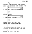
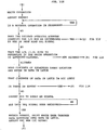
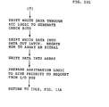
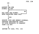
- FIGS. 11A and 11B describe a read operation in which two memory cycles are not required to perform the operation.
- FIG. 11C constitutes a branch of the sequence from FIG. 11B if an error is detected in the error correction code Logic 91 (FIG. 3).
- FIGS. 11D through 11H are flow diagrams describing the sequence that the memory controller 30 utilizes to perform a read operation requiring two memory references to complete the transfer.
- FIGS. 11I and 11J constitute flow diagrams depicting the sequence that memory controller 30 uses to execute a READ operation in which the translated address from the central processor unit 10 identifies the input/output bus 16.
- FIGS. 11K through 11M depict a sequence used by memory controller 30 to perform a WRITE operation in which the ALIGNED LW aligned longword signal from AND gate 302 (FIG. 10C) is asserted.
- FIGS. 11N and 110 depict a sequence used by memory controller 30 to perform a WRITE operation in which the ALIGNED LW aligned longword signal from AND gate 302 (FIG. 10C) is not asserted.
- FIGS. 11P and 11Q depict a sequence used by memory controller 30 to transmit write data from the central processor unit 10 to the input/output bus 16.
- FIGS. 11A through 11Q depict the detailed sequence by which the memory controller responds to memory commands from central processor unit 10. This sequence is defined in the indicated figures, and need not be described here.
Applications Claiming Priority (2)
| Application Number | Priority Date | Filing Date | Title |
|---|---|---|---|
| US06/370,572 US4500958A (en) | 1982-04-21 | 1982-04-21 | Memory controller with data rotation arrangement |
| US370572 | 1982-04-21 |
Publications (3)
| Publication Number | Publication Date |
|---|---|
| EP0099620A2 true EP0099620A2 (fr) | 1984-02-01 |
| EP0099620A3 EP0099620A3 (en) | 1986-01-22 |
| EP0099620B1 EP0099620B1 (fr) | 1990-05-30 |
Family
ID=23460240
Family Applications (1)
| Application Number | Title | Priority Date | Filing Date |
|---|---|---|---|
| EP83302250A Expired - Lifetime EP0099620B1 (fr) | 1982-04-21 | 1983-04-20 | Unité de commande de mémoire à dispositif de rotation de données |
Country Status (6)
| Country | Link |
|---|---|
| US (1) | US4500958A (fr) |
| EP (1) | EP0099620B1 (fr) |
| JP (2) | JPS5916063A (fr) |
| AU (1) | AU565868B2 (fr) |
| CA (1) | CA1190325A (fr) |
| DE (1) | DE3381621D1 (fr) |
Cited By (4)
| Publication number | Priority date | Publication date | Assignee | Title |
|---|---|---|---|---|
| EP0187762A1 (fr) * | 1984-06-27 | 1986-07-23 | Motorola, Inc. | Procede et appareil pour instructions de zone binaire |
| EP0225059A2 (fr) | 1985-10-30 | 1987-06-10 | Kabushiki Kaisha Toshiba | Mémoire à semi-conducteur |
| EP0304615A2 (fr) * | 1987-07-24 | 1989-03-01 | Kabushiki Kaisha Toshiba | Processeur de réarrangement de données |
| EP1019829A1 (fr) * | 1997-09-30 | 2000-07-19 | Idea Corporation | Procede et appareil servant a transferer les donnees entre une pile de registres et une ressource memoire |
Families Citing this family (51)
| Publication number | Priority date | Publication date | Assignee | Title |
|---|---|---|---|---|
| JPS60223250A (ja) * | 1984-04-19 | 1985-11-07 | Toshiba Corp | 情報伝送装置 |
| JPS617967A (ja) * | 1984-06-15 | 1986-01-14 | インタ−ナショナル ビジネス マシ−ンズ コ−ポレ−ション | I/oコントロ−ラ |
| JPS61179966A (ja) * | 1985-02-04 | 1986-08-12 | 渡辺解体興業株式会社 | 高層コンクリ−ト構造体の破壊方法 |
| DE3508048A1 (de) * | 1985-03-07 | 1986-09-11 | Standard Elektrik Lorenz Ag, 7000 Stuttgart | Schnittstelleneinrichtung |
| US4821179A (en) * | 1985-08-08 | 1989-04-11 | American Telephone And Telegraph Company | Communication system configuration detection apparatus and method |
| US4851991A (en) * | 1987-02-24 | 1989-07-25 | Digital Equipment Corporation | Central processor unit for digital data processing system including write buffer management mechanism |
| US5513332A (en) * | 1988-05-31 | 1996-04-30 | Extended Systems, Inc. | Database management coprocessor for on-the-fly providing data from disk media to all without first storing data in memory therebetween |
| GB8828817D0 (en) * | 1988-12-09 | 1989-01-18 | Int Computers Ltd | Data processing apparatus |
| US5142634A (en) * | 1989-02-03 | 1992-08-25 | Digital Equipment Corporation | Branch prediction |
| US5175837A (en) * | 1989-02-03 | 1992-12-29 | Digital Equipment Corporation | Synchronizing and processing of memory access operations in multiprocessor systems using a directory of lock bits |
| US4982402A (en) * | 1989-02-03 | 1991-01-01 | Digital Equipment Corporation | Method and apparatus for detecting and correcting errors in a pipelined computer system |
| US5113515A (en) * | 1989-02-03 | 1992-05-12 | Digital Equipment Corporation | Virtual instruction cache system using length responsive decoded instruction shifting and merging with prefetch buffer outputs to fill instruction buffer |
| US5222224A (en) * | 1989-02-03 | 1993-06-22 | Digital Equipment Corporation | Scheme for insuring data consistency between a plurality of cache memories and the main memory in a multi-processor system |
| US5222223A (en) * | 1989-02-03 | 1993-06-22 | Digital Equipment Corporation | Method and apparatus for ordering and queueing multiple memory requests |
| US4965793A (en) * | 1989-02-03 | 1990-10-23 | Digital Equipment Corporation | Method and apparatus for interfacing a system control unit for a multi-processor |
| US5146564A (en) * | 1989-02-03 | 1992-09-08 | Digital Equipment Corporation | Interface between a system control unit and a service processing unit of a digital computer |
| US5043874A (en) * | 1989-02-03 | 1991-08-27 | Digital Equipment Corporation | Memory configuration for use with means for interfacing a system control unit for a multi-processor system with the system main memory |
| US5019965A (en) * | 1989-02-03 | 1991-05-28 | Digital Equipment Corporation | Method and apparatus for increasing the data storage rate of a computer system having a predefined data path width |
| US4995041A (en) * | 1989-02-03 | 1991-02-19 | Digital Equipment Corporation | Write back buffer with error correcting capabilities |
| JP2616182B2 (ja) * | 1990-08-29 | 1997-06-04 | 三菱電機株式会社 | データ処理装置 |
| JP2836283B2 (ja) * | 1991-04-11 | 1998-12-14 | 日本電気株式会社 | バッファ管理方式 |
| US5257391A (en) * | 1991-08-16 | 1993-10-26 | Ncr Corporation | Disk controller having host interface and bus switches for selecting buffer and drive busses respectively based on configuration control signals |
| US5361339A (en) * | 1992-05-04 | 1994-11-01 | Xerox Corporation | Circuit for fast page mode addressing of a RAM with multiplexed row and column address lines |
| US5752216A (en) * | 1994-07-06 | 1998-05-12 | Dimensions International, Inc. | Non-intrusive data interface system for air traffic control |
| DE10202032A1 (de) * | 2002-01-18 | 2003-07-31 | Giesecke & Devrient Gmbh | Laden und Interpretieren von Daten |
| US7609567B2 (en) * | 2005-06-24 | 2009-10-27 | Metaram, Inc. | System and method for simulating an aspect of a memory circuit |
| US10013371B2 (en) | 2005-06-24 | 2018-07-03 | Google Llc | Configurable memory circuit system and method |
| US8335894B1 (en) | 2008-07-25 | 2012-12-18 | Google Inc. | Configurable memory system with interface circuit |
| US8438328B2 (en) | 2008-02-21 | 2013-05-07 | Google Inc. | Emulation of abstracted DIMMs using abstracted DRAMs |
| US8130560B1 (en) | 2006-11-13 | 2012-03-06 | Google Inc. | Multi-rank partial width memory modules |
| US8386722B1 (en) | 2008-06-23 | 2013-02-26 | Google Inc. | Stacked DIMM memory interface |
| US8077535B2 (en) | 2006-07-31 | 2011-12-13 | Google Inc. | Memory refresh apparatus and method |
| US20080082763A1 (en) | 2006-10-02 | 2008-04-03 | Metaram, Inc. | Apparatus and method for power management of memory circuits by a system or component thereof |
| US8089795B2 (en) | 2006-02-09 | 2012-01-03 | Google Inc. | Memory module with memory stack and interface with enhanced capabilities |
| US8041881B2 (en) | 2006-07-31 | 2011-10-18 | Google Inc. | Memory device with emulated characteristics |
| US8111566B1 (en) | 2007-11-16 | 2012-02-07 | Google, Inc. | Optimal channel design for memory devices for providing a high-speed memory interface |
| US8359187B2 (en) * | 2005-06-24 | 2013-01-22 | Google Inc. | Simulating a different number of memory circuit devices |
| US7386656B2 (en) | 2006-07-31 | 2008-06-10 | Metaram, Inc. | Interface circuit system and method for performing power management operations in conjunction with only a portion of a memory circuit |
| US8055833B2 (en) | 2006-10-05 | 2011-11-08 | Google Inc. | System and method for increasing capacity, performance, and flexibility of flash storage |
| US9171585B2 (en) | 2005-06-24 | 2015-10-27 | Google Inc. | Configurable memory circuit system and method |
| US8244971B2 (en) | 2006-07-31 | 2012-08-14 | Google Inc. | Memory circuit system and method |
| US8327104B2 (en) | 2006-07-31 | 2012-12-04 | Google Inc. | Adjusting the timing of signals associated with a memory system |
| US8397013B1 (en) | 2006-10-05 | 2013-03-12 | Google Inc. | Hybrid memory module |
| US8060774B2 (en) | 2005-06-24 | 2011-11-15 | Google Inc. | Memory systems and memory modules |
| US9507739B2 (en) | 2005-06-24 | 2016-11-29 | Google Inc. | Configurable memory circuit system and method |
| US8081474B1 (en) | 2007-12-18 | 2011-12-20 | Google Inc. | Embossed heat spreader |
| US8796830B1 (en) | 2006-09-01 | 2014-08-05 | Google Inc. | Stackable low-profile lead frame package |
| WO2007028109A2 (fr) | 2005-09-02 | 2007-03-08 | Metaram, Inc. | Procedes et dispositifs d'empilement de memoires dram |
| US9632929B2 (en) * | 2006-02-09 | 2017-04-25 | Google Inc. | Translating an address associated with a command communicated between a system and memory circuits |
| EP2441007A1 (fr) | 2009-06-09 | 2012-04-18 | Google, Inc. | Programmation de valeurs de résistance de terminaison dimm |
| US11132251B2 (en) | 2012-05-31 | 2021-09-28 | Samsung Electronics Co., Ltd. | Enhanced checksum system |
Citations (7)
| Publication number | Priority date | Publication date | Assignee | Title |
|---|---|---|---|---|
| US3440615A (en) * | 1966-08-22 | 1969-04-22 | Ibm | Overlapping boundary storage |
| GB1197418A (en) * | 1969-02-05 | 1970-07-01 | Ibm | Data Storage Apparatus |
| GB1218656A (en) * | 1968-03-27 | 1971-01-06 | Int Computers Ltd | Improvements in or relating to computer system |
| US3916388A (en) * | 1974-05-30 | 1975-10-28 | Ibm | Shifting apparatus for automatic data alignment |
| GB1478513A (en) * | 1974-07-01 | 1977-07-06 | Philips Electronic Associated | Memory system |
| GB2021823A (en) * | 1978-05-30 | 1979-12-05 | Intel Corp | Data transfer system |
| US4234918A (en) * | 1977-05-31 | 1980-11-18 | Burroughs Corporation | Time-shared, multi-phase memory system with error checking and data correcting |
Family Cites Families (7)
| Publication number | Priority date | Publication date | Assignee | Title |
|---|---|---|---|---|
| JPS4998537A (fr) * | 1973-01-22 | 1974-09-18 | ||
| JPS5099239A (fr) * | 1973-12-28 | 1975-08-06 | ||
| JPS54122039A (en) * | 1978-03-15 | 1979-09-21 | Toshiba Corp | Electronic computer |
| US4296467A (en) * | 1978-07-03 | 1981-10-20 | Honeywell Information Systems Inc. | Rotating chip selection technique and apparatus |
| US4298929A (en) * | 1979-01-26 | 1981-11-03 | International Business Machines Corporation | Integrated multilevel storage hierarchy for a data processing system with improved channel to memory write capability |
| JPS55118170A (en) * | 1979-03-06 | 1980-09-10 | Mitsubishi Electric Corp | Memory access device |
| JPS5755464A (en) * | 1980-09-22 | 1982-04-02 | Hitachi Ltd | Storage control device |
-
1982
- 1982-04-21 US US06/370,572 patent/US4500958A/en not_active Expired - Lifetime
-
1983
- 1983-04-13 AU AU13501/83A patent/AU565868B2/en not_active Ceased
- 1983-04-20 DE DE8383302250T patent/DE3381621D1/de not_active Expired - Fee Related
- 1983-04-20 CA CA000426297A patent/CA1190325A/fr not_active Expired
- 1983-04-20 EP EP83302250A patent/EP0099620B1/fr not_active Expired - Lifetime
- 1983-05-11 JP JP58070856A patent/JPS5916063A/ja active Pending
-
1990
- 1990-05-28 JP JP1990055874U patent/JPH02143645U/ja active Pending
Patent Citations (7)
| Publication number | Priority date | Publication date | Assignee | Title |
|---|---|---|---|---|
| US3440615A (en) * | 1966-08-22 | 1969-04-22 | Ibm | Overlapping boundary storage |
| GB1218656A (en) * | 1968-03-27 | 1971-01-06 | Int Computers Ltd | Improvements in or relating to computer system |
| GB1197418A (en) * | 1969-02-05 | 1970-07-01 | Ibm | Data Storage Apparatus |
| US3916388A (en) * | 1974-05-30 | 1975-10-28 | Ibm | Shifting apparatus for automatic data alignment |
| GB1478513A (en) * | 1974-07-01 | 1977-07-06 | Philips Electronic Associated | Memory system |
| US4234918A (en) * | 1977-05-31 | 1980-11-18 | Burroughs Corporation | Time-shared, multi-phase memory system with error checking and data correcting |
| GB2021823A (en) * | 1978-05-30 | 1979-12-05 | Intel Corp | Data transfer system |
Cited By (8)
| Publication number | Priority date | Publication date | Assignee | Title |
|---|---|---|---|---|
| EP0187762A1 (fr) * | 1984-06-27 | 1986-07-23 | Motorola, Inc. | Procede et appareil pour instructions de zone binaire |
| EP0187762A4 (fr) * | 1984-06-27 | 1987-10-19 | Motorola Inc | Procede et appareil pour instructions de zone binaire. |
| EP0225059A2 (fr) | 1985-10-30 | 1987-06-10 | Kabushiki Kaisha Toshiba | Mémoire à semi-conducteur |
| EP0225059A3 (en) * | 1985-10-30 | 1989-09-20 | Kabushiki Kaisha Toshiba | Semiconductor memory |
| EP0304615A2 (fr) * | 1987-07-24 | 1989-03-01 | Kabushiki Kaisha Toshiba | Processeur de réarrangement de données |
| EP0304615A3 (fr) * | 1987-07-24 | 1991-02-06 | Kabushiki Kaisha Toshiba | Processeur de réarrangement de données |
| EP1019829A1 (fr) * | 1997-09-30 | 2000-07-19 | Idea Corporation | Procede et appareil servant a transferer les donnees entre une pile de registres et une ressource memoire |
| EP1019829A4 (fr) * | 1997-09-30 | 2003-04-16 | Idea Corp | Procede et appareil servant a transferer les donnees entre une pile de registres et une ressource memoire |
Also Published As
| Publication number | Publication date |
|---|---|
| CA1190325A (fr) | 1985-07-09 |
| EP0099620A3 (en) | 1986-01-22 |
| DE3381621D1 (de) | 1990-07-05 |
| AU1350183A (en) | 1983-10-27 |
| US4500958A (en) | 1985-02-19 |
| AU565868B2 (en) | 1987-10-01 |
| JPH02143645U (fr) | 1990-12-05 |
| EP0099620B1 (fr) | 1990-05-30 |
| JPS5916063A (ja) | 1984-01-27 |
Similar Documents
| Publication | Publication Date | Title |
|---|---|---|
| US4500958A (en) | Memory controller with data rotation arrangement | |
| US4509115A (en) | Two-port memory controller | |
| US4229791A (en) | Distributed arbitration circuitry for data processing system | |
| EP0063334B1 (fr) | Appareil de traitement de données pour un système de multiprocesseur | |
| US4232366A (en) | Bus for a data processing system with overlapped sequences | |
| US4025906A (en) | Apparatus for identifying the type of devices coupled to a data processing system controller | |
| US4003033A (en) | Architecture for a microprogrammed device controller | |
| US4028668A (en) | Apparatus for selectively addressing sections and locations in a device controller's memory | |
| US4124891A (en) | Memory access system | |
| US4236207A (en) | Memory initialization circuit | |
| US4319323A (en) | Communications device for data processing system | |
| US4488217A (en) | Data processing system with lock-unlock instruction facility | |
| US4323967A (en) | Local bus interface for controlling information transfers between units in a central subsystem | |
| US4378591A (en) | Memory management unit for developing multiple physical addresses in parallel for use in a cache memory | |
| EP0139563B1 (fr) | Mécanisme de commande pour système multi-processeur | |
| EP0139569A2 (fr) | Mécanisme d'arbitration pour assigner la commande d'une voie de communication dans un système ordinateur (numérique) | |
| US3447135A (en) | Peripheral data exchange | |
| EP0036185B1 (fr) | Système de traitement d'information incorporant une unité de commande arithmétique formée sur une seule puce par application d'un circuit semiconducteur à haute intégration | |
| GB2075226A (en) | Cpu-to-memory interface unit | |
| GB1588806A (en) | Input/output system for a multiprocessor system | |
| US4115854A (en) | Channel bus controller | |
| US4261033A (en) | Communications processor employing line-dedicated memory tables for supervising data transfers | |
| US4322846A (en) | Self-evaluation system for determining the operational integrity of a data processing system | |
| EP0301610B1 (fr) | Appareil de traitement de données pour raccordement avec un bus de communication commun dans un système de traitement de données | |
| US5228127A (en) | Clustered multiprocessor system with global controller connected to each cluster memory control unit for directing order from processor to different cluster processors |
Legal Events
| Date | Code | Title | Description |
|---|---|---|---|
| PUAI | Public reference made under article 153(3) epc to a published international application that has entered the european phase |
Free format text: ORIGINAL CODE: 0009012 |
|
| AK | Designated contracting states |
Designated state(s): DE FR GB IT NL SE |
|
| PUAL | Search report despatched |
Free format text: ORIGINAL CODE: 0009013 |
|
| AK | Designated contracting states |
Designated state(s): DE FR GB IT NL SE |
|
| 17P | Request for examination filed |
Effective date: 19860703 |
|
| 17Q | First examination report despatched |
Effective date: 19870320 |
|
| GRAA | (expected) grant |
Free format text: ORIGINAL CODE: 0009210 |
|
| AK | Designated contracting states |
Kind code of ref document: B1 Designated state(s): DE FR GB IT NL SE |
|
| ITF | It: translation for a ep patent filed |
Owner name: JACOBACCI & PERANI S.P.A. |
|
| REF | Corresponds to: |
Ref document number: 3381621 Country of ref document: DE Date of ref document: 19900705 |
|
| ET | Fr: translation filed | ||
| PLBE | No opposition filed within time limit |
Free format text: ORIGINAL CODE: 0009261 |
|
| STAA | Information on the status of an ep patent application or granted ep patent |
Free format text: STATUS: NO OPPOSITION FILED WITHIN TIME LIMIT |
|
| 26N | No opposition filed | ||
| ITTA | It: last paid annual fee | ||
| PGFP | Annual fee paid to national office [announced via postgrant information from national office to epo] |
Ref country code: SE Payment date: 19941019 Year of fee payment: 12 |
|
| EAL | Se: european patent in force in sweden |
Ref document number: 83302250.2 |
|
| PG25 | Lapsed in a contracting state [announced via postgrant information from national office to epo] |
Ref country code: SE Effective date: 19950421 |
|
| EUG | Se: european patent has lapsed |
Ref document number: 83302250.2 |
|
| PGFP | Annual fee paid to national office [announced via postgrant information from national office to epo] |
Ref country code: NL Payment date: 19990331 Year of fee payment: 17 Ref country code: FR Payment date: 19990331 Year of fee payment: 17 |
|
| PGFP | Annual fee paid to national office [announced via postgrant information from national office to epo] |
Ref country code: GB Payment date: 19990401 Year of fee payment: 17 |
|
| PGFP | Annual fee paid to national office [announced via postgrant information from national office to epo] |
Ref country code: DE Payment date: 19990402 Year of fee payment: 17 |
|
| PG25 | Lapsed in a contracting state [announced via postgrant information from national office to epo] |
Ref country code: GB Free format text: LAPSE BECAUSE OF NON-PAYMENT OF DUE FEES Effective date: 20000420 |
|
| REG | Reference to a national code |
Ref country code: GB Ref legal event code: 732E |
|
| PG25 | Lapsed in a contracting state [announced via postgrant information from national office to epo] |
Ref country code: NL Free format text: LAPSE BECAUSE OF NON-PAYMENT OF DUE FEES Effective date: 20001101 |
|
| GBPC | Gb: european patent ceased through non-payment of renewal fee |
Effective date: 20000420 |
|
| PG25 | Lapsed in a contracting state [announced via postgrant information from national office to epo] |
Ref country code: FR Free format text: LAPSE BECAUSE OF NON-PAYMENT OF DUE FEES Effective date: 20001229 |
|
| NLV4 | Nl: lapsed or anulled due to non-payment of the annual fee |
Effective date: 20001101 |
|
| PG25 | Lapsed in a contracting state [announced via postgrant information from national office to epo] |
Ref country code: DE Free format text: LAPSE BECAUSE OF NON-PAYMENT OF DUE FEES Effective date: 20010201 |
|
| REG | Reference to a national code |
Ref country code: FR Ref legal event code: ST |