EP0098164A2 - Dispositif de mémoire semi-conductrice statique - Google Patents
Dispositif de mémoire semi-conductrice statique Download PDFInfo
- Publication number
- EP0098164A2 EP0098164A2 EP83303761A EP83303761A EP0098164A2 EP 0098164 A2 EP0098164 A2 EP 0098164A2 EP 83303761 A EP83303761 A EP 83303761A EP 83303761 A EP83303761 A EP 83303761A EP 0098164 A2 EP0098164 A2 EP 0098164A2
- Authority
- EP
- European Patent Office
- Prior art keywords
- clock signal
- signal
- bit lines
- word
- row
- Prior art date
- Legal status (The legal status is an assumption and is not a legal conclusion. Google has not performed a legal analysis and makes no representation as to the accuracy of the status listed.)
- Granted
Links
Images


Classifications
-
- G—PHYSICS
- G11—INFORMATION STORAGE
- G11C—STATIC STORES
- G11C8/00—Arrangements for selecting an address in a digital store
- G11C8/18—Address timing or clocking circuits; Address control signal generation or management, e.g. for row address strobe [RAS] or column address strobe [CAS] signals
-
- G—PHYSICS
- G11—INFORMATION STORAGE
- G11C—STATIC STORES
- G11C11/00—Digital stores characterised by the use of particular electric or magnetic storage elements; Storage elements therefor
- G11C11/21—Digital stores characterised by the use of particular electric or magnetic storage elements; Storage elements therefor using electric elements
- G11C11/34—Digital stores characterised by the use of particular electric or magnetic storage elements; Storage elements therefor using electric elements using semiconductor devices
- G11C11/40—Digital stores characterised by the use of particular electric or magnetic storage elements; Storage elements therefor using electric elements using semiconductor devices using transistors
- G11C11/41—Digital stores characterised by the use of particular electric or magnetic storage elements; Storage elements therefor using electric elements using semiconductor devices using transistors forming static cells with positive feedback, i.e. cells not needing refreshing or charge regeneration, e.g. bistable multivibrator or Schmitt trigger
- G11C11/413—Auxiliary circuits, e.g. for addressing, decoding, driving, writing, sensing, timing or power reduction
- G11C11/417—Auxiliary circuits, e.g. for addressing, decoding, driving, writing, sensing, timing or power reduction for memory cells of the field-effect type
- G11C11/418—Address circuits
-
- G—PHYSICS
- G11—INFORMATION STORAGE
- G11C—STATIC STORES
- G11C7/00—Arrangements for writing information into, or reading information out from, a digital store
- G11C7/22—Read-write [R-W] timing or clocking circuits; Read-write [R-W] control signal generators or management
Definitions
- the present invention relates to metal-oxide semiconductor (MOS) static-type semiconductor memory device.
- MOS metal-oxide semiconductor
- one static-type memory cell constructed as a flip-flop is provided at each intersection of word line and bit line pairs, and one word line and one bit line are selected by address means,-such as row address buffers, row address decoders, column address buffers, column address decoders, and the like, so that one memory cell is selected.
- address means such as row address buffers, row address decoders, column address buffers, column address decoders, and the like.
- the actual selection of one word line is performed by a word-line driver clock signal after the row address decoders determine a selected row.
- a large number of non-selected memory cells connected to the selected word line are also electrically connected to corresponding bit line pairs.
- 127 non-selected memory cells are electrically connected to corresponding bit lines.
- the dissipation of power of a static type semiconductor memory device is mainly due to the driving of such a bit line load.
- the word-line driver clock signal in a selected state, i.e., after external signals (such as a row access strobe signal) are received, the word-line driver clock signal becomes high so that at least one of the word lines is always in a selected state. Therefore, the dissipation of power is remarkably large.
- bit line pairs are connected, via load transistors, to a power supply. Therefore, in a non-selected mode, the bit line pairs are charged at a predetermined potential by the power supply. Contrary to this, in a selected mode, such as a read mode, memory cells connected to a selected word line are electrically connected to the corresponding bit line pairs so that current flows from the bit lines into the memory cells. As the result, a difference in potential between the bit lines is generated, the difference in potential is sensed or amplified by a sense amplifier, and data output is transmitted, via an output buffer, to the exterior.
- a static-type semiconductor memory device comprises a first and second power supply terminal; a plurality of word lines; a plurality of pairs of bit lines; a plurality of load means, each connected to one of said bit lines and to said first power supply terminal, for charging said bit lines;
- the present invention provides a static-type semiconductor memory device in which the dissipation of power is reduced and the read operation speed is enhanced. Since the word-line driver clock signal is generated only during a predetermined time period after the change of address information. That is, the selection time period of a word line is reduced, and, accordingly, the current flowing from the bit lines into the memory cells is also reduced. Thus, the dissipation of power is reduced. In addition, even in a previous read cycle, when the selection time period passes, the potential of each bit line remains high. Therefore, the read operation speed is dependent upon only the change of one bit line potential from a high level to a low level, which change further helps to enhance the read operation speed.
- Fig. 1 which illustrates one embodiment of the present invention
- Each memory cell is connected to one word line and a pair of bit lines.
- a memory cell C O0 is connected.to a word line WL 0 and to bit lines BL 0 and BL O .
- Selection of the word lines WL 0 , WL 1 , ---, WL n-1 is performed by the row-seleciton signals X 0 , X 1 , ---, X n-1 of row address decoders RD.
- the generation of above-mentioned row-selection signals X o , X 1 , ---, X n-1 requires the generation of a word-line driver clock signal ⁇ W of a word line driver WD.
- bit lines BL 0 , BL 0 , BL 1 , BL 1 , ---, BL n-1 , BL n-1 are connected to column-selection gates Q BO ' QB 0 ', Q B1 ' Q B1 ', ---, Q B,n-1 , Q B,n-1 ', respectively, and each gate pair is controlled by column-selection signals Y 0 , Y 1 , ---, Y n-1 .
- the selection of the bit line paris is performed by the column-selction signals Y 0 , Y 1 , ---, Y n-1 of column address decoders CD, and, in this case, the column address decoders CD decode the address signals A 0 ', A 0 ', ---, A l-1 ', A l-1 '.
- a pair of bit lines is connected, via selected column-selection gates, to data bit lines DB and DB.
- a sense amplifier SA is connected to the data bit lines DB and DB, and an output buffer OB is connected to the outputs of the sense amplifier SA.
- the word line driver WD is set by the rise of a clock signal CP 1 of a clock signal-generating circuit CK 1 and is reset by the rise of a clock signal CP 2 of a clock signal-generating circuit CK 2 .
- the clock signal--generating circuit CK 1 detects the change of the address signals A 0 , A 1 , ---, A l-1 ,A 0 ', A 1 ', ---, A l-1 ' and generates the clock signal CP 1 while the clock singal-generating circuit CP 2 detects the rise of the row-selection signals X 0 , X 1 , ---, X n-1 .
- the clock signal-generating circuit CK 2 is located at the terminals of the word lines WL O , WL 1 , ---, WL n-1 on the oppostie side of the row address decoders RD. That is, the colck signal-generating circuit CK 2 detects the timing of a row-selection signal when it propagates to the terminal of the corresponding word line, with the result that the colck signal CP 2 is generated.
- each memory cell comprises loads R 1 and R 2 , cross-coupled driver transistors Q 1 and Q 2 constituting a flip-flop, and transfer gate transistors Q 3 and Q 4 .
- the transfer gate transistors Q 3 and Q 4 are connected to the bit lines BL 0 and BL 0 (or BL 1 and BL 1 ), respectively. These transistors are turned on and off by the row-selection signal X 0 ( or Xl) at the word line WL 0 (or WL I ).
- a current I L0 flows from the bit line BL 0 to the on-state transistor Q 1 of the memory cell C 00
- a current I L1 flows from the bit line B L1 to the on-state transistor Q 1 of the memory cell C 01 . That is, in this case, even when the memory cell C 00 is selected, a current flows through the non-selected memory cell C 01 . In a 16K bit memory, the number of such non-selected cells is 127. Therefore, a reduction of the above-mentioned current is advantageous in respect to'the dissipation of power. In the present invention, even when a word line such as WL 0 is in a selected state, the duration of the high potential of the row-selection signal X 0 is limited so as to reduce the dissipation of power.
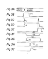
- Fig. 3A when one of the address signals A 0 , A 1 , ---, A l-1 , A 0 ', A 1 ', ---, A l-1 ' changes, the clock signal-generating circuit CK 1 detects such a change and.generates the clock signal CP 1 shown in Fig. 3B. As a result, the word-line driver WD is set so as to generate the word-line diver clock signal ⁇ W , and, subsequently, the row-selection signal of a selected word line is changed as shown in Fig. 3D.
- the potential at the terminal of the selected word line is changed from low to high.
- the clock signal-generating circuit CK 2 detects such a change and generates a clock signal CP 2 as shown in Fig. 3E.
- the word line driver WD is reset, and, accordingly, the word-line driver clock signal ⁇ W becomes low as shown in Fig. 3D. Therefore, the selected state of a word line is maintained only between the rise of the clock signal CP 1 and the rise of the clock signal CP 2 .
- the selected bit line pair is connected, by one of the column--selection signals Y 0 , Y 1 , ---, Y n-1 , to the data bit line pair DB and DB, whose potentials change as shown in Fig. 3F.
- the potentials of the data bit line pair DB and DB are amplified by the sense amplifier SA, which, in turn, generates sense data SD and SD.
- the sense data SD and SD are maintained in a latch circuit of the output buffer OB.
- the data of the latch circuit, defined by D and D are shown in Fig. 3H, and the data output D OUT of the output buffer OB is shown in Fig. 31.
- the determination of the data D and D of the latch circuit is performed between the rise of the clock signal CP 1 and the rise of the clock signal CP 2 , it is unnecessary to maintain the selected state of a word line after the generation of the clock signal CP 2 .
- the selected state of a word line is no longer maintained after the generation of the clock signal CP 2 , thereby reducing the dissipation of power of the memory cells.
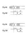
- the potentials of the data bit lines DB and DB are both high at the end of the previous address cycle since the word-line driver clock signal ⁇ W remains low, thereby helping to enhance the read operation speed, which is explained with reference to Figs. 4A, 4B, 5A, and 5B. That is, in the prior art, in a selected mode, the word-line driver clock signal ⁇ W always remains high, and, accordingly, the potential of one of the data bit lines DB and DB is high while the potential of the other is low. Therefore, if the address is changed as shown in Fig. 4A, the potentials of the data bit lines DB and DB may be reversed as shown in Fig. 4B.
- the read operation speed is dependent upon the time period ⁇ t 1 determined by the intersection of the potentials of the data bit lines DB and DB.
- the read operation speed is dependent upon the time period ⁇ t 2 determined by the point of separation of the potentials of the data bit lines DB and DB.
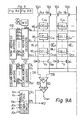
- Fig. 6 which illustrates the word line driver WD of Fig. 1
- Q41 and Q 42 are load transistors
- Q43 and Q 44 are transistors constituting a flip-flop
- Q 45 and Q 46 are input transistors. That is, the clock signal CP 1 serves as a set signal, and the clock signal CP 2 serves as a reset signal. Therefore, the word-line driver clock signal ⁇ W is set by the rise of the clock signal CP 1 and is reset by the rise of the clock signal CP 2 .
- the clock signal-generating circuit CK 1 comprises a plurality of signal-generating circuits PG1, corresponding to each of the address signals A 0 , A 1 , ---, A l-1 , A 0 ', A 1 ', ---, A l-1 ', and an OR gate OR1.
- the signal-generating circuits PG1 detect a change of the address signal and generate a pulse having a predetermined time period.
- the signal--generating circuit PG1 comprises NAND gates G 1 through G 4 , NOR gates G 5 and G 6 , an OR gate G 7 , and capacitors C 1 and C 2 .
- the gates G 1 , G 2 , and G 5 and the capacitor C 1 form a rise-detecting circuit
- the gates G 1 , G 3 , G 4 , and G 6 and the capacitor C 2 form a fall-detecting circuit. Therefore, the output of the gate G 7 detects the rise and fall of the address signal A i , i.e., the change thereof, and generates the signal CP l .
- the address signal A i node a
- the output b of the NAND gate G 1 changes and the output d of the NAND gate G 2 is an inverted signal of the signal b, which is delayed a little by the capacitor C 1 .
- the output f of the NOR gate G 5 is a pulse which is generated by the rise of the address signal A.
- the output g of the NOR gate G 6 is a signal which is generated by the fall of the address signal A.
- the output h of the OR gate G 7 which combines the signal f with the signal g, is a clock signal which is generated by the change of the address signal A i .
- a signal-generating circuit PG1 as illustrated in Fig. 7B is provided for each address signal, and, accordingly, the clock signal-generating circuit CK 1 generates a clock signal CP 1 when any one of the address signals is changed.
- the clock signal-generating circuit CK 2 comprises a plurality of signal-generating circuits PG2, corresponding to the row address signals X 1 , X 2 , ---, X n-1 , and an OR gate OR2.
- the signal-generating circuits PG2 detect a rise in the address signal and generate a signal having a predetermined time period.
- the signal-generating circuit PG2 shown in Fig. 8B comprises NAND gates G 8 , G 9 , an OR gate G 10 , and a capacitor C 3 .
- the output buffer OB is controlled by the clock signal CP 1 of the clock signal-generating circuit CK 1 , and the load transistors Q L0 , Q L0 ', Q L1 , Q L1 ', ---, Q L,n-1 , Q L,n-1 ' are controlled by an inverted signal CP 2 of the clock signal CP 2 of the clock signal--generating circuit CK 2 .
- the signal CP 2 is obtained by an inverter I 0 .
- the clock signal CP 1 controls the output buffer OB so that the data output D OUT thereof is temporarily maintained at a high level when an address is changed and thereafter to obtain an essentially effective data output so as to enhance the read operation speed.
- the data output D OUT of the output buffer is maintained at a high level for a predetermined time period regardless of the potentials of the sense data SD and SD of the sense amplifier SA. That is, as is shown in Figs. 11A and 11B, the clock signal CP 1 is generated during a predetermined time period T after the time to when the address is changed. By using this clock signal CP 1 , the latch data D is caused to assume a high level and the latch data D is caused to assume a low level, as is shown in Fig. 11C.
- the data output D OUT of the output buffer is pushed up or maintained regardless of the potential of the sense data SD and SD, as is illustrated in Fig. 11D.
- this potential changes only from a high level to a low level. Therefore, the read operation speed is dependent upon the time period At 4 and, accordingly, is high.
- Fig. 12 which illustrates the output buffer OB of Fig. 9, the sense data SD is supplied to an inverter I 1 formed by a depletion-type transistor Q 121 and an enhancement-type transistor Q122 while the sense data SD is supplied to an'inverter I 2 formed by a depletion-type transistor Q 123 and an enhancement-type transistor Q 124 .
- the output of the inverter I 1 is connected to a charging transistor Q 125 of an inverter I 3
- the output of the inverter 1 2 is a discharging transistor Q126 of the inverter I 3 .
- a transistor Q 127 is connected to the input side of the inverter I 1
- a transistor Q 128 is connected to the output of the inverter I 2 .
- These transistors Q 127 and Q 128 are controlled by the clock signal CP 1 of the clock signal-generating circuit CK 1 .
- the clock signal CP 1 is at a low level.
- the potential of the sense data SD is inverted by the inverter I 1
- the potential of the sense data SD is inverted by the inverter I 2 . Therefore, usually, since the sense data SD is at a high level while the sense data SD is at a low level or vice versa, one of the transistors Q 125 and Q 126 is in an on-state while the other is in an off-state. For example, when the transistor Q 125 is in an on-state, the data output D OUT becomes high due to the charging operation of the transistor Q5.
- the data output D OUT becomes low due to the discharging operation of the transistor Q 126 . That is, the potential of the data output D OUT changes in accordance with a change,in the potential of the sense data SD and SD.
- the transistor Q 127 When the clock signal CP 1 is at a high level, the transistor Q 127 is turned on so that the input of the inverter I 1 becomes low while the output of the inverter I 1 becomes high. As a result, the transistor Q 125 is turned on. That is, the charging transistor Q 125 is turned on regardless of the potential of the sense data SD. Simultaneously, since the transistor Q 128 is turned on, the output of the inverter I 2 becomes low, and, accordingly, the dis- charging transistor Q126 is turned off. That is, the discharging transistor Q 126 is turned off regardless of the potential of the sense data SD. As a result the data output D OUT becomes high.
- bit lines BL 0 , BL O , BL 1 , 1 ---, BL n-1 , BL n-1 are disconnected from the power supply V CC , the difference in potential between the bit lines is rapidly increased, as is indicated by the dotted line in Fig. 5B, thereby improving the read operation speed.
- control of the load transistors is effective particularly when the memory cells located near the clock signal-generating circuit are selected since the signal CP 2 begins to fall after the terminal potential of a word line rises.
Landscapes
- Engineering & Computer Science (AREA)
- Microelectronics & Electronic Packaging (AREA)
- Computer Hardware Design (AREA)
- Static Random-Access Memory (AREA)
- Dram (AREA)
Applications Claiming Priority (6)
| Application Number | Priority Date | Filing Date | Title |
|---|---|---|---|
| JP111519/82 | 1982-06-30 | ||
| JP111523/82 | 1982-06-30 | ||
| JP57111523A JPS593783A (ja) | 1982-06-30 | 1982-06-30 | 半導体記憶装置 |
| JP57111519A JPS593781A (ja) | 1982-06-30 | 1982-06-30 | スタテイツク型半導体記憶装置 |
| JP57111535A JPS593786A (ja) | 1982-06-30 | 1982-06-30 | スタテイツク型半導体記憶装置 |
| JP111535/82 | 1982-06-30 |
Publications (3)
| Publication Number | Publication Date |
|---|---|
| EP0098164A2 true EP0098164A2 (fr) | 1984-01-11 |
| EP0098164A3 EP0098164A3 (en) | 1986-02-05 |
| EP0098164B1 EP0098164B1 (fr) | 1989-01-11 |
Family
ID=27311981
Family Applications (1)
| Application Number | Title | Priority Date | Filing Date |
|---|---|---|---|
| EP83303761A Expired EP0098164B1 (fr) | 1982-06-30 | 1983-06-29 | Dispositif de mémoire semi-conductrice statique |
Country Status (3)
| Country | Link |
|---|---|
| US (1) | US4539661A (fr) |
| EP (1) | EP0098164B1 (fr) |
| DE (1) | DE3378939D1 (fr) |
Cited By (6)
| Publication number | Priority date | Publication date | Assignee | Title |
|---|---|---|---|---|
| EP0178914A2 (fr) * | 1984-10-16 | 1986-04-23 | Mitsubishi Denki Kabushiki Kaisha | Dispositif de mémoire semi-conductrice |
| EP0190823A2 (fr) * | 1985-01-31 | 1986-08-13 | International Business Machines Corporation | Circuit de précharge |
| EP0262995A2 (fr) * | 1986-08-07 | 1988-04-06 | Fujitsu Limited | Dispositif à mémoires à semi-conducteurs avec un circuit de détection de transitions d'adresses |
| FR2619939A1 (fr) * | 1987-09-01 | 1989-03-03 | Thomson Semiconducteurs | Circuit de detection de transitions d'adresses |
| EP0415408A2 (fr) * | 1989-08-30 | 1991-03-06 | Nec Corporation | Dispositif de mémoire à semi-conducteurs du type MOS |
| EP0533096A2 (fr) * | 1991-09-17 | 1993-03-24 | Nec Corporation | Système pour adresser sans multi-sélection des lignes de mots |
Families Citing this family (8)
| Publication number | Priority date | Publication date | Assignee | Title |
|---|---|---|---|---|
| US4712194A (en) * | 1984-06-08 | 1987-12-08 | Matsushita Electric Industrial Co., Ltd. | Static random access memory |
| JP2569554B2 (ja) * | 1987-05-13 | 1997-01-08 | 三菱電機株式会社 | ダイナミツクram |
| US5615168A (en) * | 1995-10-02 | 1997-03-25 | International Business Machines Corporation | Method and apparatus for synchronized pipeline data access of a memory system |
| US6038634A (en) * | 1998-02-02 | 2000-03-14 | International Business Machines Corporation | Intra-unit block addressing system for memory |
| US6262936B1 (en) | 1998-03-13 | 2001-07-17 | Cypress Semiconductor Corp. | Random access memory having independent read port and write port and process for writing to and reading from the same |
| US6262937B1 (en) | 1998-03-13 | 2001-07-17 | Cypress Semiconductor Corp. | Synchronous random access memory having a read/write address bus and process for writing to and reading from the same |
| US6069839A (en) | 1998-03-20 | 2000-05-30 | Cypress Semiconductor Corp. | Circuit and method for implementing single-cycle read/write operation(s), and random access memory including the circuit and/or practicing the method |
| NO312928B1 (no) * | 2001-02-26 | 2002-07-15 | Thin Film Electronics Asa | Ikke-destruktiv utlesing |
Citations (5)
| Publication number | Priority date | Publication date | Assignee | Title |
|---|---|---|---|---|
| FR2184865A1 (fr) * | 1972-05-16 | 1973-12-28 | Nippon Electric Co | |
| US3859637A (en) * | 1973-06-28 | 1975-01-07 | Ibm | On-chip auxiliary latch for down-powering array latch decoders |
| JPS5532207A (en) * | 1978-08-23 | 1980-03-06 | Fujitsu Ltd | Manufacture of information board |
| EP0043245A2 (fr) * | 1980-06-30 | 1982-01-06 | Inmos Corporation | Mémoire statique à accès aléatoire équilibrée et préchargée de façon asynchrone |
| US4328558A (en) * | 1978-03-09 | 1982-05-04 | Motorola, Inc. | RAM Address enable circuit for a microprocessor having an on-chip RAM |
Family Cites Families (3)
| Publication number | Priority date | Publication date | Assignee | Title |
|---|---|---|---|---|
| JPS55135392A (en) * | 1979-04-04 | 1980-10-22 | Nec Corp | Memory circuit |
| JPS56130885A (en) * | 1980-03-18 | 1981-10-14 | Fujitsu Ltd | Address buffer circuit |
| US4480320A (en) * | 1982-06-01 | 1984-10-30 | General Instrument Corp. | Compact ROM with reduced access time |
-
1983
- 1983-06-28 US US06/508,505 patent/US4539661A/en not_active Expired - Fee Related
- 1983-06-29 EP EP83303761A patent/EP0098164B1/fr not_active Expired
- 1983-06-29 DE DE8383303761T patent/DE3378939D1/de not_active Expired
Patent Citations (5)
| Publication number | Priority date | Publication date | Assignee | Title |
|---|---|---|---|---|
| FR2184865A1 (fr) * | 1972-05-16 | 1973-12-28 | Nippon Electric Co | |
| US3859637A (en) * | 1973-06-28 | 1975-01-07 | Ibm | On-chip auxiliary latch for down-powering array latch decoders |
| US4328558A (en) * | 1978-03-09 | 1982-05-04 | Motorola, Inc. | RAM Address enable circuit for a microprocessor having an on-chip RAM |
| JPS5532207A (en) * | 1978-08-23 | 1980-03-06 | Fujitsu Ltd | Manufacture of information board |
| EP0043245A2 (fr) * | 1980-06-30 | 1982-01-06 | Inmos Corporation | Mémoire statique à accès aléatoire équilibrée et préchargée de façon asynchrone |
Non-Patent Citations (1)
| Title |
|---|
| PATENTS ABSTRACTS OF JAPAN, vol. 4, no. 62 (P-10)[544], 9th May 1980; & JP - A - 55 32207 (FUJITSU K.K.) 06-03-1980 * |
Cited By (13)
| Publication number | Priority date | Publication date | Assignee | Title |
|---|---|---|---|---|
| EP0178914A3 (en) * | 1984-10-16 | 1987-09-30 | Mitsubishi Denki Kabushiki Kaisha | A semiconductor memory device a semiconductor memory device |
| EP0178914A2 (fr) * | 1984-10-16 | 1986-04-23 | Mitsubishi Denki Kabushiki Kaisha | Dispositif de mémoire semi-conductrice |
| EP0190823A3 (en) * | 1985-01-31 | 1989-10-25 | International Business Machines Corporation | Precharge circuit |
| EP0190823A2 (fr) * | 1985-01-31 | 1986-08-13 | International Business Machines Corporation | Circuit de précharge |
| EP0262995A2 (fr) * | 1986-08-07 | 1988-04-06 | Fujitsu Limited | Dispositif à mémoires à semi-conducteurs avec un circuit de détection de transitions d'adresses |
| EP0262995B1 (fr) * | 1986-08-07 | 1996-03-27 | Fujitsu Limited | Dispositif à mémoires à semi-conducteurs avec un circuit de détection de transitions d'adresses |
| EP0306392A1 (fr) * | 1987-09-01 | 1989-03-08 | STMicroelectronics S.A. | Circuit de détection de transitions d'adresses |
| FR2619939A1 (fr) * | 1987-09-01 | 1989-03-03 | Thomson Semiconducteurs | Circuit de detection de transitions d'adresses |
| US4922122A (en) * | 1987-09-01 | 1990-05-01 | Sgs-Thomson Microelectronics, Sa | Circuit for the detection of address transitions |
| EP0415408A2 (fr) * | 1989-08-30 | 1991-03-06 | Nec Corporation | Dispositif de mémoire à semi-conducteurs du type MOS |
| EP0415408A3 (en) * | 1989-08-30 | 1993-05-05 | Nec Corporation | Mos type semiconductor memory device |
| EP0533096A2 (fr) * | 1991-09-17 | 1993-03-24 | Nec Corporation | Système pour adresser sans multi-sélection des lignes de mots |
| EP0533096A3 (en) * | 1991-09-17 | 1995-04-19 | Nippon Electric Co | Addressing system free from multi-selection of word lines |
Also Published As
| Publication number | Publication date |
|---|---|
| DE3378939D1 (en) | 1989-02-16 |
| US4539661A (en) | 1985-09-03 |
| EP0098164A3 (en) | 1986-02-05 |
| EP0098164B1 (fr) | 1989-01-11 |
Similar Documents
| Publication | Publication Date | Title |
|---|---|---|
| US4766572A (en) | Semiconductor memory having a bypassable data output latch | |
| US4817057A (en) | Semiconductor memory device having improved precharge scheme | |
| US6791897B2 (en) | Word line driving circuit | |
| EP0098164A2 (fr) | Dispositif de mémoire semi-conductrice statique | |
| JPH0652685A (ja) | パワーオンリセット制御型ラッチ型行ラインリピータを有する半導体メモリ | |
| EP0051920A2 (fr) | Dispositif de mémoire ayant des moyens de connexion à une unité de processeur centrale | |
| JPS62287499A (ja) | 半導体メモリ装置 | |
| JPH0454318B2 (fr) | ||
| EP0115140B1 (fr) | Circuit décodeur | |
| EP0050037B1 (fr) | Dispositif de mémoire semiconductrice | |
| JPS6120078B2 (fr) | ||
| EP0259862B1 (fr) | Mémoire à semi-conducteurs avec fonction d'écriture | |
| US6067264A (en) | High speed semiconductor memory device | |
| EP0031995B1 (fr) | Dispositif de mémoire à semi-conducteurs comprenant une matrice de cellules de mémoire statiques | |
| US6466508B1 (en) | Semiconductor memory device having high-speed read function | |
| EP0083195A2 (fr) | Circuit décodeur pour un dispositif semi-conducteur | |
| JPS6160515B2 (fr) | ||
| US6396746B2 (en) | Semiconductor memory device | |
| EP0148364B1 (fr) | Générateur de signal de référence temporelle | |
| EP1193714B1 (fr) | Bascule multiplexeur sélecteur de banc très rapide | |
| US5034924A (en) | Static random access memory device with pull-down control circuit | |
| US5337287A (en) | Dual port semiconductor memory device | |
| EP0170912A2 (fr) | Circuit intégré avec une borne d'entrée commune | |
| JPS6216472B2 (fr) | ||
| US5563840A (en) | Integrated semiconductor device |
Legal Events
| Date | Code | Title | Description |
|---|---|---|---|
| PUAI | Public reference made under article 153(3) epc to a published international application that has entered the european phase |
Free format text: ORIGINAL CODE: 0009012 |
|
| AK | Designated contracting states |
Designated state(s): DE FR GB |
|
| PUAL | Search report despatched |
Free format text: ORIGINAL CODE: 0009013 |
|
| AK | Designated contracting states |
Designated state(s): DE FR GB |
|
| 17P | Request for examination filed |
Effective date: 19860218 |
|
| 17Q | First examination report despatched |
Effective date: 19870512 |
|
| GRAA | (expected) grant |
Free format text: ORIGINAL CODE: 0009210 |
|
| AK | Designated contracting states |
Kind code of ref document: B1 Designated state(s): DE FR GB |
|
| REF | Corresponds to: |
Ref document number: 3378939 Country of ref document: DE Date of ref document: 19890216 |
|
| ET | Fr: translation filed | ||
| PLBE | No opposition filed within time limit |
Free format text: ORIGINAL CODE: 0009261 |
|
| STAA | Information on the status of an ep patent application or granted ep patent |
Free format text: STATUS: NO OPPOSITION FILED WITHIN TIME LIMIT |
|
| 26N | No opposition filed | ||
| PGFP | Annual fee paid to national office [announced via postgrant information from national office to epo] |
Ref country code: FR Payment date: 19960611 Year of fee payment: 14 |
|
| PGFP | Annual fee paid to national office [announced via postgrant information from national office to epo] |
Ref country code: GB Payment date: 19960620 Year of fee payment: 14 |
|
| PGFP | Annual fee paid to national office [announced via postgrant information from national office to epo] |
Ref country code: DE Payment date: 19960627 Year of fee payment: 14 |
|
| PG25 | Lapsed in a contracting state [announced via postgrant information from national office to epo] |
Ref country code: GB Free format text: LAPSE BECAUSE OF NON-PAYMENT OF DUE FEES Effective date: 19970629 |
|
| GBPC | Gb: european patent ceased through non-payment of renewal fee |
Effective date: 19970629 |
|
| PG25 | Lapsed in a contracting state [announced via postgrant information from national office to epo] |
Ref country code: FR Free format text: LAPSE BECAUSE OF NON-PAYMENT OF DUE FEES Effective date: 19980227 |
|
| PG25 | Lapsed in a contracting state [announced via postgrant information from national office to epo] |
Ref country code: DE Free format text: LAPSE BECAUSE OF NON-PAYMENT OF DUE FEES Effective date: 19980303 |
|
| REG | Reference to a national code |
Ref country code: FR Ref legal event code: ST |
|
| REG | Reference to a national code |
Ref country code: FR Ref legal event code: ST |