EP0097503B1 - Verfahren zur Herstellung einer Flachdruckplatte - Google Patents
Verfahren zur Herstellung einer Flachdruckplatte Download PDFInfo
- Publication number
- EP0097503B1 EP0097503B1 EP83303514A EP83303514A EP0097503B1 EP 0097503 B1 EP0097503 B1 EP 0097503B1 EP 83303514 A EP83303514 A EP 83303514A EP 83303514 A EP83303514 A EP 83303514A EP 0097503 B1 EP0097503 B1 EP 0097503B1
- Authority
- EP
- European Patent Office
- Prior art keywords
- printing plate
- process according
- chromium
- layer
- support
- Prior art date
- Legal status (The legal status is an assumption and is not a legal conclusion. Google has not performed a legal analysis and makes no representation as to the accuracy of the status listed.)
- Expired
Links
- 238000007639 printing Methods 0.000 title claims description 164
- 238000004519 manufacturing process Methods 0.000 title claims description 11
- VYZAMTAEIAYCRO-UHFFFAOYSA-N Chromium Chemical compound [Cr] VYZAMTAEIAYCRO-UHFFFAOYSA-N 0.000 claims description 71
- XEEYBQQBJWHFJM-UHFFFAOYSA-N Iron Chemical compound [Fe] XEEYBQQBJWHFJM-UHFFFAOYSA-N 0.000 claims description 67
- 239000011651 chromium Substances 0.000 claims description 66
- 229910052804 chromium Inorganic materials 0.000 claims description 65
- 238000000034 method Methods 0.000 claims description 50
- 239000000203 mixture Substances 0.000 claims description 43
- XLYOFNOQVPJJNP-UHFFFAOYSA-N water Substances O XLYOFNOQVPJJNP-UHFFFAOYSA-N 0.000 claims description 36
- 239000013078 crystal Substances 0.000 claims description 35
- 229910052742 iron Inorganic materials 0.000 claims description 34
- 239000000758 substrate Substances 0.000 claims description 22
- QVGXLLKOCUKJST-UHFFFAOYSA-N atomic oxygen Chemical compound [O] QVGXLLKOCUKJST-UHFFFAOYSA-N 0.000 claims description 18
- 229910052760 oxygen Inorganic materials 0.000 claims description 18
- 239000001301 oxygen Substances 0.000 claims description 18
- 239000003792 electrolyte Substances 0.000 claims description 16
- 239000011248 coating agent Substances 0.000 claims description 15
- 238000000576 coating method Methods 0.000 claims description 15
- 239000007788 liquid Substances 0.000 claims description 8
- KRVSOGSZCMJSLX-UHFFFAOYSA-L chromic acid Substances O[Cr](O)(=O)=O KRVSOGSZCMJSLX-UHFFFAOYSA-L 0.000 claims description 7
- AWJWCTOOIBYHON-UHFFFAOYSA-N furo[3,4-b]pyrazine-5,7-dione Chemical compound C1=CN=C2C(=O)OC(=O)C2=N1 AWJWCTOOIBYHON-UHFFFAOYSA-N 0.000 claims description 7
- 150000001553 barium compounds Chemical class 0.000 claims description 3
- 238000004070 electrodeposition Methods 0.000 claims 1
- 239000010410 layer Substances 0.000 description 102
- 239000000463 material Substances 0.000 description 62
- 239000000047 product Substances 0.000 description 33
- 239000000243 solution Substances 0.000 description 33
- -1 argon ion Chemical class 0.000 description 31
- 229920005989 resin Polymers 0.000 description 27
- 239000011347 resin Substances 0.000 description 27
- 239000000126 substance Substances 0.000 description 27
- 239000000839 emulsion Substances 0.000 description 22
- WSFSSNUMVMOOMR-UHFFFAOYSA-N Formaldehyde Chemical compound O=C WSFSSNUMVMOOMR-UHFFFAOYSA-N 0.000 description 21
- 238000011161 development Methods 0.000 description 20
- 229910052709 silver Inorganic materials 0.000 description 18
- 239000004332 silver Substances 0.000 description 18
- 229910000831 Steel Inorganic materials 0.000 description 16
- 238000001035 drying Methods 0.000 description 16
- 239000010959 steel Substances 0.000 description 16
- 238000012360 testing method Methods 0.000 description 16
- 150000001875 compounds Chemical class 0.000 description 14
- 238000005406 washing Methods 0.000 description 14
- 238000005530 etching Methods 0.000 description 13
- HEMHJVSKTPXQMS-UHFFFAOYSA-M Sodium hydroxide Chemical compound [OH-].[Na+] HEMHJVSKTPXQMS-UHFFFAOYSA-M 0.000 description 12
- 238000004458 analytical method Methods 0.000 description 10
- 125000004429 atom Chemical group 0.000 description 10
- 239000013047 polymeric layer Substances 0.000 description 10
- KFZMGEQAYNKOFK-UHFFFAOYSA-N Isopropanol Chemical compound CC(C)O KFZMGEQAYNKOFK-UHFFFAOYSA-N 0.000 description 9
- 230000000052 comparative effect Effects 0.000 description 9
- 239000002245 particle Substances 0.000 description 8
- 150000003839 salts Chemical class 0.000 description 8
- OKTJSMMVPCPJKN-UHFFFAOYSA-N Carbon Chemical compound [C] OKTJSMMVPCPJKN-UHFFFAOYSA-N 0.000 description 7
- 229910000975 Carbon steel Inorganic materials 0.000 description 7
- 229910052799 carbon Inorganic materials 0.000 description 7
- CSCPPACGZOOCGX-UHFFFAOYSA-N Acetone Chemical compound CC(C)=O CSCPPACGZOOCGX-UHFFFAOYSA-N 0.000 description 6
- VEXZGXHMUGYJMC-UHFFFAOYSA-M Chloride anion Chemical compound [Cl-] VEXZGXHMUGYJMC-UHFFFAOYSA-M 0.000 description 6
- PXHVJJICTQNCMI-UHFFFAOYSA-N Nickel Chemical compound [Ni] PXHVJJICTQNCMI-UHFFFAOYSA-N 0.000 description 6
- 239000003795 chemical substances by application Substances 0.000 description 6
- 229910052751 metal Inorganic materials 0.000 description 6
- 239000002184 metal Substances 0.000 description 6
- 150000002989 phenols Chemical class 0.000 description 6
- 229920000642 polymer Polymers 0.000 description 6
- 238000002203 pretreatment Methods 0.000 description 6
- 238000012545 processing Methods 0.000 description 6
- 229920001577 copolymer Polymers 0.000 description 5
- 230000007797 corrosion Effects 0.000 description 5
- 238000005260 corrosion Methods 0.000 description 5
- 125000000664 diazo group Chemical group [N-]=[N+]=[*] 0.000 description 5
- 238000005868 electrolysis reaction Methods 0.000 description 5
- 238000005259 measurement Methods 0.000 description 5
- 230000035945 sensitivity Effects 0.000 description 5
- KETQAJRQOHHATG-UHFFFAOYSA-N 1,2-naphthoquinone Chemical compound C1=CC=C2C(=O)C(=O)C=CC2=C1 KETQAJRQOHHATG-UHFFFAOYSA-N 0.000 description 4
- ISWSIDIOOBJBQZ-UHFFFAOYSA-N Phenol Chemical compound OC1=CC=CC=C1 ISWSIDIOOBJBQZ-UHFFFAOYSA-N 0.000 description 4
- 239000004372 Polyvinyl alcohol Substances 0.000 description 4
- BQCADISMDOOEFD-UHFFFAOYSA-N Silver Chemical compound [Ag] BQCADISMDOOEFD-UHFFFAOYSA-N 0.000 description 4
- 229910021607 Silver chloride Inorganic materials 0.000 description 4
- 239000004115 Sodium Silicate Substances 0.000 description 4
- XLOMVQKBTHCTTD-UHFFFAOYSA-N Zinc monoxide Chemical compound [Zn]=O XLOMVQKBTHCTTD-UHFFFAOYSA-N 0.000 description 4
- HUMNYLRZRPPJDN-UHFFFAOYSA-N benzaldehyde Chemical compound O=CC1=CC=CC=C1 HUMNYLRZRPPJDN-UHFFFAOYSA-N 0.000 description 4
- 239000010962 carbon steel Substances 0.000 description 4
- 238000013016 damping Methods 0.000 description 4
- 238000010894 electron beam technology Methods 0.000 description 4
- 125000002887 hydroxy group Chemical group [H]O* 0.000 description 4
- 238000010884 ion-beam technique Methods 0.000 description 4
- 229910001507 metal halide Inorganic materials 0.000 description 4
- 150000005309 metal halides Chemical class 0.000 description 4
- 239000000178 monomer Substances 0.000 description 4
- 229920000728 polyester Polymers 0.000 description 4
- 229920001296 polysiloxane Polymers 0.000 description 4
- 229920002451 polyvinyl alcohol Polymers 0.000 description 4
- 238000002360 preparation method Methods 0.000 description 4
- 229920002379 silicone rubber Polymers 0.000 description 4
- 239000004945 silicone rubber Substances 0.000 description 4
- HKZLPVFGJNLROG-UHFFFAOYSA-M silver monochloride Chemical compound [Cl-].[Ag+] HKZLPVFGJNLROG-UHFFFAOYSA-M 0.000 description 4
- SQGYOTSLMSWVJD-UHFFFAOYSA-N silver(1+) nitrate Chemical compound [Ag+].[O-]N(=O)=O SQGYOTSLMSWVJD-UHFFFAOYSA-N 0.000 description 4
- 235000011121 sodium hydroxide Nutrition 0.000 description 4
- NTHWMYGWWRZVTN-UHFFFAOYSA-N sodium silicate Chemical compound [Na+].[Na+].[O-][Si]([O-])=O NTHWMYGWWRZVTN-UHFFFAOYSA-N 0.000 description 4
- 229910052911 sodium silicate Inorganic materials 0.000 description 4
- 239000007787 solid Substances 0.000 description 4
- QTWJRLJHJPIABL-UHFFFAOYSA-N 2-methylphenol;3-methylphenol;4-methylphenol Chemical compound CC1=CC=C(O)C=C1.CC1=CC=CC(O)=C1.CC1=CC=CC=C1O QTWJRLJHJPIABL-UHFFFAOYSA-N 0.000 description 3
- FUGYGGDSWSUORM-UHFFFAOYSA-N 4-hydroxystyrene Chemical compound OC1=CC=C(C=C)C=C1 FUGYGGDSWSUORM-UHFFFAOYSA-N 0.000 description 3
- IMNFDUFMRHMDMM-UHFFFAOYSA-N N-Heptane Chemical compound CCCCCCC IMNFDUFMRHMDMM-UHFFFAOYSA-N 0.000 description 3
- MUBZPKHOEPUJKR-UHFFFAOYSA-N Oxalic acid Chemical compound OC(=O)C(O)=O MUBZPKHOEPUJKR-UHFFFAOYSA-N 0.000 description 3
- YXFVVABEGXRONW-UHFFFAOYSA-N Toluene Chemical compound CC1=CC=CC=C1 YXFVVABEGXRONW-UHFFFAOYSA-N 0.000 description 3
- WGLPBDUCMAPZCE-UHFFFAOYSA-N Trioxochromium Chemical compound O=[Cr](=O)=O WGLPBDUCMAPZCE-UHFFFAOYSA-N 0.000 description 3
- 150000001299 aldehydes Chemical class 0.000 description 3
- 229910052782 aluminium Inorganic materials 0.000 description 3
- XAGFODPZIPBFFR-UHFFFAOYSA-N aluminium Chemical compound [Al] XAGFODPZIPBFFR-UHFFFAOYSA-N 0.000 description 3
- 239000011230 binding agent Substances 0.000 description 3
- 230000015572 biosynthetic process Effects 0.000 description 3
- IISBACLAFKSPIT-UHFFFAOYSA-N bisphenol A Chemical compound C=1C=C(O)C=CC=1C(C)(C)C1=CC=C(O)C=C1 IISBACLAFKSPIT-UHFFFAOYSA-N 0.000 description 3
- OIPQUBBCOVJSNS-UHFFFAOYSA-L bromo(iodo)silver Chemical compound Br[Ag]I OIPQUBBCOVJSNS-UHFFFAOYSA-L 0.000 description 3
- 125000002915 carbonyl group Chemical group [*:2]C([*:1])=O 0.000 description 3
- UOUJSJZBMCDAEU-UHFFFAOYSA-N chromium(3+);oxygen(2-) Chemical class [O-2].[O-2].[O-2].[Cr+3].[Cr+3] UOUJSJZBMCDAEU-UHFFFAOYSA-N 0.000 description 3
- 239000008199 coating composition Substances 0.000 description 3
- 229930003836 cresol Natural products 0.000 description 3
- 230000001747 exhibiting effect Effects 0.000 description 3
- 150000002576 ketones Chemical class 0.000 description 3
- 229910052759 nickel Inorganic materials 0.000 description 3
- 238000007645 offset printing Methods 0.000 description 3
- 125000004430 oxygen atom Chemical group O* 0.000 description 3
- 229920001568 phenolic resin Polymers 0.000 description 3
- NLKNQRATVPKPDG-UHFFFAOYSA-M potassium iodide Chemical compound [K+].[I-] NLKNQRATVPKPDG-UHFFFAOYSA-M 0.000 description 3
- 239000002244 precipitate Substances 0.000 description 3
- 238000000682 scanning probe acoustic microscopy Methods 0.000 description 3
- 230000001235 sensitizing effect Effects 0.000 description 3
- 235000019795 sodium metasilicate Nutrition 0.000 description 3
- 238000003892 spreading Methods 0.000 description 3
- 239000004094 surface-active agent Substances 0.000 description 3
- 238000012546 transfer Methods 0.000 description 3
- 230000009466 transformation Effects 0.000 description 3
- XNWFRZJHXBZDAG-UHFFFAOYSA-N 2-METHOXYETHANOL Chemical compound COCCO XNWFRZJHXBZDAG-UHFFFAOYSA-N 0.000 description 2
- ZRYCRPNCXLQHPN-UHFFFAOYSA-N 3-hydroxy-2-methylbenzaldehyde Chemical compound CC1=C(O)C=CC=C1C=O ZRYCRPNCXLQHPN-UHFFFAOYSA-N 0.000 description 2
- IKHGUXGNUITLKF-UHFFFAOYSA-N Acetaldehyde Chemical compound CC=O IKHGUXGNUITLKF-UHFFFAOYSA-N 0.000 description 2
- IJGRMHOSHXDMSA-UHFFFAOYSA-N Atomic nitrogen Chemical compound N#N IJGRMHOSHXDMSA-UHFFFAOYSA-N 0.000 description 2
- 238000000864 Auger spectrum Methods 0.000 description 2
- VEXZGXHMUGYJMC-UHFFFAOYSA-N Hydrochloric acid Chemical compound Cl VEXZGXHMUGYJMC-UHFFFAOYSA-N 0.000 description 2
- DGAQECJNVWCQMB-PUAWFVPOSA-M Ilexoside XXIX Chemical compound C[C@@H]1CC[C@@]2(CC[C@@]3(C(=CC[C@H]4[C@]3(CC[C@@H]5[C@@]4(CC[C@@H](C5(C)C)OS(=O)(=O)[O-])C)C)[C@@H]2[C@]1(C)O)C)C(=O)O[C@H]6[C@@H]([C@H]([C@@H]([C@H](O6)CO)O)O)O.[Na+] DGAQECJNVWCQMB-PUAWFVPOSA-M 0.000 description 2
- OFOBLEOULBTSOW-UHFFFAOYSA-N Malonic acid Chemical compound OC(=O)CC(O)=O OFOBLEOULBTSOW-UHFFFAOYSA-N 0.000 description 2
- NBIIXXVUZAFLBC-UHFFFAOYSA-N Phosphoric acid Chemical compound OP(O)(O)=O NBIIXXVUZAFLBC-UHFFFAOYSA-N 0.000 description 2
- 239000004793 Polystyrene Substances 0.000 description 2
- FAPWRFPIFSIZLT-UHFFFAOYSA-M Sodium chloride Chemical compound [Na+].[Cl-] FAPWRFPIFSIZLT-UHFFFAOYSA-M 0.000 description 2
- 229920002125 Sokalan® Polymers 0.000 description 2
- PPBRXRYQALVLMV-UHFFFAOYSA-N Styrene Chemical compound C=CC1=CC=CC=C1 PPBRXRYQALVLMV-UHFFFAOYSA-N 0.000 description 2
- QAOWNCQODCNURD-UHFFFAOYSA-N Sulfuric acid Chemical compound OS(O)(=O)=O QAOWNCQODCNURD-UHFFFAOYSA-N 0.000 description 2
- 239000002253 acid Substances 0.000 description 2
- 230000002378 acidificating effect Effects 0.000 description 2
- 239000003513 alkali Substances 0.000 description 2
- 229910045601 alloy Inorganic materials 0.000 description 2
- 239000000956 alloy Substances 0.000 description 2
- 239000007864 aqueous solution Substances 0.000 description 2
- XKRFYHLGVUSROY-UHFFFAOYSA-N argon Substances [Ar] XKRFYHLGVUSROY-UHFFFAOYSA-N 0.000 description 2
- 229910052786 argon Inorganic materials 0.000 description 2
- 125000003118 aryl group Chemical group 0.000 description 2
- HRBFQSUTUDRTSV-UHFFFAOYSA-N benzene-1,2,3-triol;propan-2-one Chemical compound CC(C)=O.OC1=CC=CC(O)=C1O HRBFQSUTUDRTSV-UHFFFAOYSA-N 0.000 description 2
- 238000004364 calculation method Methods 0.000 description 2
- 239000003054 catalyst Substances 0.000 description 2
- 239000007795 chemical reaction product Substances 0.000 description 2
- 238000009833 condensation Methods 0.000 description 2
- 230000005494 condensation Effects 0.000 description 2
- 239000012954 diazonium Substances 0.000 description 2
- BJZIJOLEWHWTJO-UHFFFAOYSA-H dipotassium;hexafluorozirconium(2-) Chemical compound [F-].[F-].[F-].[F-].[F-].[F-].[K+].[K+].[Zr+4] BJZIJOLEWHWTJO-UHFFFAOYSA-H 0.000 description 2
- 238000000921 elemental analysis Methods 0.000 description 2
- 238000005886 esterification reaction Methods 0.000 description 2
- 150000002148 esters Chemical class 0.000 description 2
- 239000007789 gas Substances 0.000 description 2
- 238000005227 gel permeation chromatography Methods 0.000 description 2
- 238000010438 heat treatment Methods 0.000 description 2
- 150000002500 ions Chemical class 0.000 description 2
- 150000002505 iron Chemical class 0.000 description 2
- QSHDDOUJBYECFT-UHFFFAOYSA-N mercury Chemical compound [Hg] QSHDDOUJBYECFT-UHFFFAOYSA-N 0.000 description 2
- XZSZONUJSGDIFI-UHFFFAOYSA-N n-(4-hydroxyphenyl)-2-methylprop-2-enamide Chemical compound CC(=C)C(=O)NC1=CC=C(O)C=C1 XZSZONUJSGDIFI-UHFFFAOYSA-N 0.000 description 2
- 239000012860 organic pigment Substances 0.000 description 2
- QNGNSVIICDLXHT-UHFFFAOYSA-N para-ethylbenzaldehyde Natural products CCC1=CC=C(C=O)C=C1 QNGNSVIICDLXHT-UHFFFAOYSA-N 0.000 description 2
- 238000007747 plating Methods 0.000 description 2
- 239000004584 polyacrylic acid Substances 0.000 description 2
- 229920002223 polystyrene Polymers 0.000 description 2
- IOLCXVTUBQKXJR-UHFFFAOYSA-M potassium bromide Chemical compound [K+].[Br-] IOLCXVTUBQKXJR-UHFFFAOYSA-M 0.000 description 2
- 238000010298 pulverizing process Methods 0.000 description 2
- WQGWDDDVZFFDIG-UHFFFAOYSA-N pyrogallol Chemical compound OC1=CC=CC(O)=C1O WQGWDDDVZFFDIG-UHFFFAOYSA-N 0.000 description 2
- 239000001397 quillaja saponaria molina bark Substances 0.000 description 2
- 229930182490 saponin Natural products 0.000 description 2
- 150000007949 saponins Chemical class 0.000 description 2
- 229910001961 silver nitrate Inorganic materials 0.000 description 2
- 239000011734 sodium Substances 0.000 description 2
- 229910052708 sodium Inorganic materials 0.000 description 2
- 239000002904 solvent Substances 0.000 description 2
- 238000004611 spectroscopical analysis Methods 0.000 description 2
- 238000005507 spraying Methods 0.000 description 2
- 238000003756 stirring Methods 0.000 description 2
- 229920002554 vinyl polymer Polymers 0.000 description 2
- 239000011787 zinc oxide Substances 0.000 description 2
- PJMXUSNWBKGQEZ-UHFFFAOYSA-N (4-hydroxyphenyl) 2-methylprop-2-enoate Chemical compound CC(=C)C(=O)OC1=CC=C(O)C=C1 PJMXUSNWBKGQEZ-UHFFFAOYSA-N 0.000 description 1
- AZQWKYJCGOJGHM-UHFFFAOYSA-N 1,4-benzoquinone Chemical compound O=C1C=CC(=O)C=C1 AZQWKYJCGOJGHM-UHFFFAOYSA-N 0.000 description 1
- ASFXKDBHBVHSLT-UHFFFAOYSA-N 1-(4-ethoxyphenyl)-2h-tetrazole-5-thione Chemical compound C1=CC(OCC)=CC=C1N1C(=S)N=NN1 ASFXKDBHBVHSLT-UHFFFAOYSA-N 0.000 description 1
- GGZHVNZHFYCSEV-UHFFFAOYSA-N 1-Phenyl-5-mercaptotetrazole Chemical compound SC1=NN=NN1C1=CC=CC=C1 GGZHVNZHFYCSEV-UHFFFAOYSA-N 0.000 description 1
- IXPNQXFRVYWDDI-UHFFFAOYSA-N 1-methyl-2,4-dioxo-1,3-diazinane-5-carboximidamide Chemical compound CN1CC(C(N)=N)C(=O)NC1=O IXPNQXFRVYWDDI-UHFFFAOYSA-N 0.000 description 1
- VZQBDGHUOBRFAA-UHFFFAOYSA-N 2-(2,6-dihydroxyphenyl)benzaldehyde Chemical compound C1(O)=C(C(O)=CC=C1)C1=CC=CC=C1C=O VZQBDGHUOBRFAA-UHFFFAOYSA-N 0.000 description 1
- JKFYKCYQEWQPTM-UHFFFAOYSA-N 2-azaniumyl-2-(4-fluorophenyl)acetate Chemical compound OC(=O)C(N)C1=CC=C(F)C=C1 JKFYKCYQEWQPTM-UHFFFAOYSA-N 0.000 description 1
- OMIGHNLMNHATMP-UHFFFAOYSA-N 2-hydroxyethyl prop-2-enoate Chemical group OCCOC(=O)C=C OMIGHNLMNHATMP-UHFFFAOYSA-N 0.000 description 1
- PSAURYCHUAGLFL-UHFFFAOYSA-N 2-prop-2-enylidenepropanedioic acid Chemical class OC(=O)C(C(O)=O)=CC=C PSAURYCHUAGLFL-UHFFFAOYSA-N 0.000 description 1
- WUPHOULIZUERAE-UHFFFAOYSA-N 3-(oxolan-2-yl)propanoic acid Chemical compound OC(=O)CCC1CCCO1 WUPHOULIZUERAE-UHFFFAOYSA-N 0.000 description 1
- WTQZSMDDRMKJRI-UHFFFAOYSA-N 4-diazoniophenolate Chemical compound [O-]C1=CC=C([N+]#N)C=C1 WTQZSMDDRMKJRI-UHFFFAOYSA-N 0.000 description 1
- RSWGJHLUYNHPMX-UHFFFAOYSA-N Abietic-Saeure Natural products C12CCC(C(C)C)=CC2=CCC2C1(C)CCCC2(C)C(O)=O RSWGJHLUYNHPMX-UHFFFAOYSA-N 0.000 description 1
- NLHHRLWOUZZQLW-UHFFFAOYSA-N Acrylonitrile Chemical compound C=CC#N NLHHRLWOUZZQLW-UHFFFAOYSA-N 0.000 description 1
- QGZKDVFQNNGYKY-UHFFFAOYSA-O Ammonium Chemical compound [NH4+] QGZKDVFQNNGYKY-UHFFFAOYSA-O 0.000 description 1
- LSNNMFCWUKXFEE-UHFFFAOYSA-M Bisulfite Chemical compound OS([O-])=O LSNNMFCWUKXFEE-UHFFFAOYSA-M 0.000 description 1
- 229910001339 C alloy Inorganic materials 0.000 description 1
- OYPRJOBELJOOCE-UHFFFAOYSA-N Calcium Chemical group [Ca] OYPRJOBELJOOCE-UHFFFAOYSA-N 0.000 description 1
- 229920002134 Carboxymethyl cellulose Polymers 0.000 description 1
- 229920000623 Cellulose acetate phthalate Polymers 0.000 description 1
- 229920000742 Cotton Polymers 0.000 description 1
- XDTMQSROBMDMFD-UHFFFAOYSA-N Cyclohexane Chemical compound C1CCCCC1 XDTMQSROBMDMFD-UHFFFAOYSA-N 0.000 description 1
- BRLQWZUYTZBJKN-UHFFFAOYSA-N Epichlorohydrin Chemical compound ClCC1CO1 BRLQWZUYTZBJKN-UHFFFAOYSA-N 0.000 description 1
- LFQSCWFLJHTTHZ-UHFFFAOYSA-N Ethanol Chemical group CCO LFQSCWFLJHTTHZ-UHFFFAOYSA-N 0.000 description 1
- JIGUQPWFLRLWPJ-UHFFFAOYSA-N Ethyl acrylate Chemical compound CCOC(=O)C=C JIGUQPWFLRLWPJ-UHFFFAOYSA-N 0.000 description 1
- 239000001856 Ethyl cellulose Substances 0.000 description 1
- 229910000640 Fe alloy Inorganic materials 0.000 description 1
- KRHYYFGTRYWZRS-UHFFFAOYSA-M Fluoride anion Chemical compound [F-] KRHYYFGTRYWZRS-UHFFFAOYSA-M 0.000 description 1
- WOBHKFSMXKNTIM-UHFFFAOYSA-N Hydroxyethyl methacrylate Chemical group CC(=C)C(=O)OCCO WOBHKFSMXKNTIM-UHFFFAOYSA-N 0.000 description 1
- 229910000617 Mangalloy Inorganic materials 0.000 description 1
- PWHULOQIROXLJO-UHFFFAOYSA-N Manganese Chemical compound [Mn] PWHULOQIROXLJO-UHFFFAOYSA-N 0.000 description 1
- CERQOIWHTDAKMF-UHFFFAOYSA-N Methacrylic acid Chemical compound CC(=C)C(O)=O CERQOIWHTDAKMF-UHFFFAOYSA-N 0.000 description 1
- ZOKXTWBITQBERF-UHFFFAOYSA-N Molybdenum Chemical compound [Mo] ZOKXTWBITQBERF-UHFFFAOYSA-N 0.000 description 1
- 229910018487 Ni—Cr Inorganic materials 0.000 description 1
- 239000004952 Polyamide Substances 0.000 description 1
- NRCMAYZCPIVABH-UHFFFAOYSA-N Quinacridone Chemical compound N1C2=CC=CC=C2C(=O)C2=C1C=C1C(=O)C3=CC=CC=C3NC1=C2 NRCMAYZCPIVABH-UHFFFAOYSA-N 0.000 description 1
- KHPCPRHQVVSZAH-HUOMCSJISA-N Rosin Natural products O(C/C=C/c1ccccc1)[C@H]1[C@H](O)[C@@H](O)[C@@H](O)[C@@H](CO)O1 KHPCPRHQVVSZAH-HUOMCSJISA-N 0.000 description 1
- 229920001800 Shellac Polymers 0.000 description 1
- 229910021612 Silver iodide Inorganic materials 0.000 description 1
- ATJFFYVFTNAWJD-UHFFFAOYSA-N Tin Chemical compound [Sn] ATJFFYVFTNAWJD-UHFFFAOYSA-N 0.000 description 1
- 238000002441 X-ray diffraction Methods 0.000 description 1
- XEIPQVVAVOUIOP-UHFFFAOYSA-N [Au]=S Chemical compound [Au]=S XEIPQVVAVOUIOP-UHFFFAOYSA-N 0.000 description 1
- DPXJVFZANSGRMM-UHFFFAOYSA-N acetic acid;2,3,4,5,6-pentahydroxyhexanal;sodium Chemical compound [Na].CC(O)=O.OCC(O)C(O)C(O)C(O)C=O DPXJVFZANSGRMM-UHFFFAOYSA-N 0.000 description 1
- 239000003929 acidic solution Substances 0.000 description 1
- 230000001154 acute effect Effects 0.000 description 1
- 239000000654 additive Substances 0.000 description 1
- 239000000853 adhesive Substances 0.000 description 1
- 230000001070 adhesive effect Effects 0.000 description 1
- 238000001856 aerosol method Methods 0.000 description 1
- 239000012670 alkaline solution Substances 0.000 description 1
- 239000004411 aluminium Substances 0.000 description 1
- 229910000147 aluminium phosphate Inorganic materials 0.000 description 1
- DIZPMCHEQGEION-UHFFFAOYSA-H aluminium sulfate (anhydrous) Chemical compound [Al+3].[Al+3].[O-]S([O-])(=O)=O.[O-]S([O-])(=O)=O.[O-]S([O-])(=O)=O DIZPMCHEQGEION-UHFFFAOYSA-H 0.000 description 1
- LDDQLRUQCUTJBB-UHFFFAOYSA-O azanium;hydrofluoride Chemical compound [NH4+].F LDDQLRUQCUTJBB-UHFFFAOYSA-O 0.000 description 1
- IVRMZWNICZWHMI-UHFFFAOYSA-N azide group Chemical group [N-]=[N+]=[N-] IVRMZWNICZWHMI-UHFFFAOYSA-N 0.000 description 1
- 230000001588 bifunctional effect Effects 0.000 description 1
- 239000007844 bleaching agent Substances 0.000 description 1
- ZEUDGVUWMXAXEF-UHFFFAOYSA-L bromo(chloro)silver Chemical compound Cl[Ag]Br ZEUDGVUWMXAXEF-UHFFFAOYSA-L 0.000 description 1
- 229910052980 cadmium sulfide Inorganic materials 0.000 description 1
- 238000011088 calibration curve Methods 0.000 description 1
- 125000004432 carbon atom Chemical group C* 0.000 description 1
- VQXINLNPICQTLR-UHFFFAOYSA-N carbonyl diazide Chemical compound [N-]=[N+]=NC(=O)N=[N+]=[N-] VQXINLNPICQTLR-UHFFFAOYSA-N 0.000 description 1
- 239000001768 carboxy methyl cellulose Substances 0.000 description 1
- 235000010948 carboxy methyl cellulose Nutrition 0.000 description 1
- 239000008112 carboxymethyl-cellulose Substances 0.000 description 1
- 229940105329 carboxymethylcellulose Drugs 0.000 description 1
- 229920002678 cellulose Polymers 0.000 description 1
- 235000010980 cellulose Nutrition 0.000 description 1
- 229920002301 cellulose acetate Polymers 0.000 description 1
- 229940081734 cellulose acetate phthalate Drugs 0.000 description 1
- ZUIVNYGZFPOXFW-UHFFFAOYSA-N chembl1717603 Chemical compound N1=C(C)C=C(O)N2N=CN=C21 ZUIVNYGZFPOXFW-UHFFFAOYSA-N 0.000 description 1
- 238000006243 chemical reaction Methods 0.000 description 1
- 125000001309 chloro group Chemical group Cl* 0.000 description 1
- VNNRSPGTAMTISX-UHFFFAOYSA-N chromium nickel Chemical compound [Cr].[Ni] VNNRSPGTAMTISX-UHFFFAOYSA-N 0.000 description 1
- 229910000423 chromium oxide Inorganic materials 0.000 description 1
- JOPOVCBBYLSVDA-UHFFFAOYSA-N chromium(6+) Chemical compound [Cr+6] JOPOVCBBYLSVDA-UHFFFAOYSA-N 0.000 description 1
- 229910017052 cobalt Inorganic materials 0.000 description 1
- 239000010941 cobalt Substances 0.000 description 1
- GUTLYIVDDKVIGB-UHFFFAOYSA-N cobalt atom Chemical compound [Co] GUTLYIVDDKVIGB-UHFFFAOYSA-N 0.000 description 1
- 239000000084 colloidal system Substances 0.000 description 1
- 239000000470 constituent Substances 0.000 description 1
- 229940013361 cresol Drugs 0.000 description 1
- 230000007547 defect Effects 0.000 description 1
- 150000001989 diazonium salts Chemical class 0.000 description 1
- 239000004205 dimethyl polysiloxane Substances 0.000 description 1
- 235000013870 dimethyl polysiloxane Nutrition 0.000 description 1
- 229920005645 diorganopolysiloxane polymer Polymers 0.000 description 1
- RXCBCUJUGULOGC-UHFFFAOYSA-H dipotassium;tetrafluorotitanium;difluoride Chemical compound [F-].[F-].[F-].[F-].[F-].[F-].[K+].[K+].[Ti+4] RXCBCUJUGULOGC-UHFFFAOYSA-H 0.000 description 1
- 238000007598 dipping method Methods 0.000 description 1
- 238000009826 distribution Methods 0.000 description 1
- 239000000975 dye Substances 0.000 description 1
- 230000000694 effects Effects 0.000 description 1
- 230000005611 electricity Effects 0.000 description 1
- 239000003822 epoxy resin Substances 0.000 description 1
- 235000019325 ethyl cellulose Nutrition 0.000 description 1
- 229920001249 ethyl cellulose Polymers 0.000 description 1
- 238000001914 filtration Methods 0.000 description 1
- 125000001153 fluoro group Chemical group F* 0.000 description 1
- 238000009472 formulation Methods 0.000 description 1
- 150000002334 glycols Chemical class 0.000 description 1
- 229910052736 halogen Inorganic materials 0.000 description 1
- 150000002367 halogens Chemical class 0.000 description 1
- LNEPOXFFQSENCJ-UHFFFAOYSA-N haloperidol Chemical compound C1CC(O)(C=2C=CC(Cl)=CC=2)CCN1CCCC(=O)C1=CC=C(F)C=C1 LNEPOXFFQSENCJ-UHFFFAOYSA-N 0.000 description 1
- 229920001519 homopolymer Polymers 0.000 description 1
- 150000004677 hydrates Chemical class 0.000 description 1
- 230000002209 hydrophobic effect Effects 0.000 description 1
- 238000007654 immersion Methods 0.000 description 1
- 235000000396 iron Nutrition 0.000 description 1
- 229910052748 manganese Inorganic materials 0.000 description 1
- 239000011572 manganese Substances 0.000 description 1
- WPBNNNQJVZRUHP-UHFFFAOYSA-L manganese(2+);methyl n-[[2-(methoxycarbonylcarbamothioylamino)phenyl]carbamothioyl]carbamate;n-[2-(sulfidocarbothioylamino)ethyl]carbamodithioate Chemical compound [Mn+2].[S-]C(=S)NCCNC([S-])=S.COC(=O)NC(=S)NC1=CC=CC=C1NC(=S)NC(=O)OC WPBNNNQJVZRUHP-UHFFFAOYSA-L 0.000 description 1
- 150000002739 metals Chemical class 0.000 description 1
- WSFSSNUMVMOOMR-NJFSPNSNSA-N methanone Chemical compound O=[14CH2] WSFSSNUMVMOOMR-NJFSPNSNSA-N 0.000 description 1
- 238000002156 mixing Methods 0.000 description 1
- 229910052750 molybdenum Inorganic materials 0.000 description 1
- 239000011733 molybdenum Substances 0.000 description 1
- POVITWJTUUJBNK-UHFFFAOYSA-N n-(4-hydroxyphenyl)prop-2-enamide Chemical group OC1=CC=C(NC(=O)C=C)C=C1 POVITWJTUUJBNK-UHFFFAOYSA-N 0.000 description 1
- 239000000025 natural resin Substances 0.000 description 1
- 229910052757 nitrogen Inorganic materials 0.000 description 1
- 125000004433 nitrogen atom Chemical group N* 0.000 description 1
- 239000003960 organic solvent Substances 0.000 description 1
- 235000006408 oxalic acid Nutrition 0.000 description 1
- 150000002916 oxazoles Chemical class 0.000 description 1
- WKMKTIVRRLOHAJ-UHFFFAOYSA-N oxygen(2-);thallium(1+) Chemical compound [O-2].[Tl+].[Tl+] WKMKTIVRRLOHAJ-UHFFFAOYSA-N 0.000 description 1
- PNJWIWWMYCMZRO-UHFFFAOYSA-N pent‐4‐en‐2‐one Natural products CC(=O)CC=C PNJWIWWMYCMZRO-UHFFFAOYSA-N 0.000 description 1
- VLTRZXGMWDSKGL-UHFFFAOYSA-N perchloric acid Chemical class OCl(=O)(=O)=O VLTRZXGMWDSKGL-UHFFFAOYSA-N 0.000 description 1
- KHIWWQKSHDUIBK-UHFFFAOYSA-N periodic acid Chemical class OI(=O)(=O)=O KHIWWQKSHDUIBK-UHFFFAOYSA-N 0.000 description 1
- 229960003742 phenol Drugs 0.000 description 1
- 239000005011 phenolic resin Substances 0.000 description 1
- IEQIEDJGQAUEQZ-UHFFFAOYSA-N phthalocyanine Chemical compound N1C(N=C2C3=CC=CC=C3C(N=C3C4=CC=CC=C4C(=N4)N3)=N2)=C(C=CC=C2)C2=C1N=C1C2=CC=CC=C2C4=N1 IEQIEDJGQAUEQZ-UHFFFAOYSA-N 0.000 description 1
- 239000000049 pigment Substances 0.000 description 1
- 239000004014 plasticizer Substances 0.000 description 1
- 229920003227 poly(N-vinyl carbazole) Polymers 0.000 description 1
- 229920000435 poly(dimethylsiloxane) Polymers 0.000 description 1
- 229920002647 polyamide Polymers 0.000 description 1
- 229920006122 polyamide resin Polymers 0.000 description 1
- 229920000515 polycarbonate Polymers 0.000 description 1
- 239000004417 polycarbonate Substances 0.000 description 1
- 229920000647 polyepoxide Polymers 0.000 description 1
- 229920006267 polyester film Polymers 0.000 description 1
- 229920000139 polyethylene terephthalate Polymers 0.000 description 1
- 239000005020 polyethylene terephthalate Substances 0.000 description 1
- 229920005749 polyurethane resin Polymers 0.000 description 1
- 239000012286 potassium permanganate Substances 0.000 description 1
- 230000002035 prolonged effect Effects 0.000 description 1
- 229940079877 pyrogallol Drugs 0.000 description 1
- WVIICGIFSIBFOG-UHFFFAOYSA-N pyrylium Chemical class C1=CC=[O+]C=C1 WVIICGIFSIBFOG-UHFFFAOYSA-N 0.000 description 1
- 239000011541 reaction mixture Substances 0.000 description 1
- GHMLBKRAJCXXBS-UHFFFAOYSA-N resorcinol Chemical compound OC1=CC=CC(O)=C1 GHMLBKRAJCXXBS-UHFFFAOYSA-N 0.000 description 1
- 229960001755 resorcinol Drugs 0.000 description 1
- 239000012266 salt solution Substances 0.000 description 1
- 238000004062 sedimentation Methods 0.000 description 1
- JPJALAQPGMAKDF-UHFFFAOYSA-N selenium dioxide Chemical compound O=[Se]=O JPJALAQPGMAKDF-UHFFFAOYSA-N 0.000 description 1
- 239000004065 semiconductor Substances 0.000 description 1
- 239000004208 shellac Substances 0.000 description 1
- 229940113147 shellac Drugs 0.000 description 1
- ZLGIYFNHBLSMPS-ATJNOEHPSA-N shellac Chemical compound OCCCCCC(O)C(O)CCCCCCCC(O)=O.C1C23[C@H](C(O)=O)CCC2[C@](C)(CO)[C@@H]1C(C(O)=O)=C[C@@H]3O ZLGIYFNHBLSMPS-ATJNOEHPSA-N 0.000 description 1
- 235000013874 shellac Nutrition 0.000 description 1
- CGFYHILWFSGVJS-UHFFFAOYSA-N silicic acid;trioxotungsten Chemical compound O[Si](O)(O)O.O=[W]1(=O)O[W](=O)(=O)O[W](=O)(=O)O1.O=[W]1(=O)O[W](=O)(=O)O[W](=O)(=O)O1.O=[W]1(=O)O[W](=O)(=O)O[W](=O)(=O)O1.O=[W]1(=O)O[W](=O)(=O)O[W](=O)(=O)O1 CGFYHILWFSGVJS-UHFFFAOYSA-N 0.000 description 1
- 229940045105 silver iodide Drugs 0.000 description 1
- 239000003707 silyl modified polymer Substances 0.000 description 1
- 239000000661 sodium alginate Substances 0.000 description 1
- 235000010413 sodium alginate Nutrition 0.000 description 1
- 229940005550 sodium alginate Drugs 0.000 description 1
- 239000011780 sodium chloride Substances 0.000 description 1
- 239000003381 stabilizer Substances 0.000 description 1
- 229910001220 stainless steel Inorganic materials 0.000 description 1
- 239000011550 stock solution Substances 0.000 description 1
- 238000000967 suction filtration Methods 0.000 description 1
- NRUVOKMCGYWODZ-UHFFFAOYSA-N sulfanylidenepalladium Chemical compound [Pd]=S NRUVOKMCGYWODZ-UHFFFAOYSA-N 0.000 description 1
- 150000003459 sulfonic acid esters Chemical class 0.000 description 1
- 150000003460 sulfonic acids Chemical class 0.000 description 1
- 125000000472 sulfonyl group Chemical group *S(*)(=O)=O 0.000 description 1
- 125000004434 sulfur atom Chemical group 0.000 description 1
- HSVFKFNNMLUVEY-UHFFFAOYSA-N sulfuryl diazide Chemical compound [N-]=[N+]=NS(=O)(=O)N=[N+]=[N-] HSVFKFNNMLUVEY-UHFFFAOYSA-N 0.000 description 1
- 229910003438 thallium oxide Inorganic materials 0.000 description 1
- KHPCPRHQVVSZAH-UHFFFAOYSA-N trans-cinnamyl beta-D-glucopyranoside Natural products OC1C(O)C(O)C(CO)OC1OCC=CC1=CC=CC=C1 KHPCPRHQVVSZAH-UHFFFAOYSA-N 0.000 description 1
- 238000000844 transformation Methods 0.000 description 1
- 230000001131 transforming effect Effects 0.000 description 1
- ZIBGPFATKBEMQZ-UHFFFAOYSA-N triethylene glycol Chemical compound OCCOCCOCCO ZIBGPFATKBEMQZ-UHFFFAOYSA-N 0.000 description 1
- 239000013638 trimer Substances 0.000 description 1
- WFKWXMTUELFFGS-UHFFFAOYSA-N tungsten Chemical compound [W] WFKWXMTUELFFGS-UHFFFAOYSA-N 0.000 description 1
- 229910052721 tungsten Inorganic materials 0.000 description 1
- 239000010937 tungsten Substances 0.000 description 1
- 229930195735 unsaturated hydrocarbon Natural products 0.000 description 1
- 238000009736 wetting Methods 0.000 description 1
- 229910052724 xenon Inorganic materials 0.000 description 1
- FHNFHKCVQCLJFQ-UHFFFAOYSA-N xenon atom Chemical compound [Xe] FHNFHKCVQCLJFQ-UHFFFAOYSA-N 0.000 description 1
Images


Classifications
-
- C—CHEMISTRY; METALLURGY
- C25—ELECTROLYTIC OR ELECTROPHORETIC PROCESSES; APPARATUS THEREFOR
- C25D—PROCESSES FOR THE ELECTROLYTIC OR ELECTROPHORETIC PRODUCTION OF COATINGS; ELECTROFORMING; APPARATUS THEREFOR
- C25D11/00—Electrolytic coating by surface reaction, i.e. forming conversion layers
- C25D11/38—Chromatising
-
- B—PERFORMING OPERATIONS; TRANSPORTING
- B41—PRINTING; LINING MACHINES; TYPEWRITERS; STAMPS
- B41N—PRINTING PLATES OR FOILS; MATERIALS FOR SURFACES USED IN PRINTING MACHINES FOR PRINTING, INKING, DAMPING, OR THE LIKE; PREPARING SUCH SURFACES FOR USE AND CONSERVING THEM
- B41N1/00—Printing plates or foils; Materials therefor
- B41N1/04—Printing plates or foils; Materials therefor metallic
- B41N1/08—Printing plates or foils; Materials therefor metallic for lithographic printing
-
- Y—GENERAL TAGGING OF NEW TECHNOLOGICAL DEVELOPMENTS; GENERAL TAGGING OF CROSS-SECTIONAL TECHNOLOGIES SPANNING OVER SEVERAL SECTIONS OF THE IPC; TECHNICAL SUBJECTS COVERED BY FORMER USPC CROSS-REFERENCE ART COLLECTIONS [XRACs] AND DIGESTS
- Y10—TECHNICAL SUBJECTS COVERED BY FORMER USPC
- Y10T—TECHNICAL SUBJECTS COVERED BY FORMER US CLASSIFICATION
- Y10T428/00—Stock material or miscellaneous articles
- Y10T428/12—All metal or with adjacent metals
- Y10T428/12493—Composite; i.e., plural, adjacent, spatially distinct metal components [e.g., layers, joint, etc.]
-
- Y—GENERAL TAGGING OF NEW TECHNOLOGICAL DEVELOPMENTS; GENERAL TAGGING OF CROSS-SECTIONAL TECHNOLOGIES SPANNING OVER SEVERAL SECTIONS OF THE IPC; TECHNICAL SUBJECTS COVERED BY FORMER USPC CROSS-REFERENCE ART COLLECTIONS [XRACs] AND DIGESTS
- Y10—TECHNICAL SUBJECTS COVERED BY FORMER USPC
- Y10T—TECHNICAL SUBJECTS COVERED BY FORMER US CLASSIFICATION
- Y10T428/00—Stock material or miscellaneous articles
- Y10T428/12—All metal or with adjacent metals
- Y10T428/12493—Composite; i.e., plural, adjacent, spatially distinct metal components [e.g., layers, joint, etc.]
- Y10T428/12535—Composite; i.e., plural, adjacent, spatially distinct metal components [e.g., layers, joint, etc.] with additional, spatially distinct nonmetal component
-
- Y—GENERAL TAGGING OF NEW TECHNOLOGICAL DEVELOPMENTS; GENERAL TAGGING OF CROSS-SECTIONAL TECHNOLOGIES SPANNING OVER SEVERAL SECTIONS OF THE IPC; TECHNICAL SUBJECTS COVERED BY FORMER USPC CROSS-REFERENCE ART COLLECTIONS [XRACs] AND DIGESTS
- Y10—TECHNICAL SUBJECTS COVERED BY FORMER USPC
- Y10T—TECHNICAL SUBJECTS COVERED BY FORMER US CLASSIFICATION
- Y10T428/00—Stock material or miscellaneous articles
- Y10T428/12—All metal or with adjacent metals
- Y10T428/12493—Composite; i.e., plural, adjacent, spatially distinct metal components [e.g., layers, joint, etc.]
- Y10T428/12535—Composite; i.e., plural, adjacent, spatially distinct metal components [e.g., layers, joint, etc.] with additional, spatially distinct nonmetal component
- Y10T428/12583—Component contains compound of adjacent metal
- Y10T428/1259—Oxide
-
- Y—GENERAL TAGGING OF NEW TECHNOLOGICAL DEVELOPMENTS; GENERAL TAGGING OF CROSS-SECTIONAL TECHNOLOGIES SPANNING OVER SEVERAL SECTIONS OF THE IPC; TECHNICAL SUBJECTS COVERED BY FORMER USPC CROSS-REFERENCE ART COLLECTIONS [XRACs] AND DIGESTS
- Y10—TECHNICAL SUBJECTS COVERED BY FORMER USPC
- Y10T—TECHNICAL SUBJECTS COVERED BY FORMER US CLASSIFICATION
- Y10T428/00—Stock material or miscellaneous articles
- Y10T428/12—All metal or with adjacent metals
- Y10T428/12493—Composite; i.e., plural, adjacent, spatially distinct metal components [e.g., layers, joint, etc.]
- Y10T428/12535—Composite; i.e., plural, adjacent, spatially distinct metal components [e.g., layers, joint, etc.] with additional, spatially distinct nonmetal component
- Y10T428/12611—Oxide-containing component
Definitions
- This invention relates to a process for preparing a lithographic printing plate having an electrodeposited chromium layer on an iron substrate.
- EP-A-0022033 discloses a process for preparing a lithographic printing plate using a pretreatment step and a main treatment step, both steps making use of electrolytes comprising anhydrous chromic acid (see page 4, lines 15-32 of this document).
- An electrolyte comprising a chromic acid is likewise disclosed in US-A-2 780 592.
- electrodeposited chromium layers including those in the form of a matt chromium deposit comprising crystalline products throughout having angles which protrude from the surface of this electrodeposited chromium layer. These layers will also include some oxygen atoms resulting from the production of gas at the electrodes.
- an object of this invention is to provide a process for preparing a lithographic printing plate which has high mechanical strength and also has sufficient adhesion to photosensitive layer, printing life and tolerance in developing methods.
- this process for preparing such a lithographic printing plate comprising coating a photosensitive composition on a support having an electrodeposited chromium layer on an iron substrate, is characterised in that said electrodeposited chromium layer, the surface of which comprises crystalline products with angles which protrude therefrom, at least 50% of the elements in the portion (hereinafter referred to as the "surface side portion") from the said surface to the depthwise position where the atomic concentration of the atoms constituting the iron substrate exceeds 20% are chromium and oxygen and the ratios of atomic concentrations of chromium and oxygen at said portion are substantially even at the same depth from every point on said surface, is produced using an electrolyte comprising 80 g of chromic acid (as Cr 2 0 3 ) per 1 liter of electrolyte to 430 g of chromic acid per 1 liter of water, for example 80 to 200 g/l, and 1 to 10 g of a barium compound per 1 liter of electrolyte.
- an electrolyte compris
- the iron material to be used in this invention may be pure iron or an alloy of iron with other elements.
- other elements forming alloys with iron there may be included carbon, manganese and nickel.
- Typical examples of the alloys may include carbon steels (alloys of carbon (0.04 to 1.7%) and iron), cast irons with higher contents of carbon than carbon steels, and further special steels (e.g. manganese steel, nickel steel, chromium steel, nickel-chromium steel) having added other elements (e.g. manganese, nickel, chromium, cobalt, tungsten, molybdenum).
- the above carbon steels may include super-soft steels (0.25% or less carbon), soft steels (0.25 to 0.5% carbon), hard steels (0.5 to 1.0% carbon) and super-hard steels (1.0% or more carbon).
- Preferred plate crystals are polygonal (primarily hexagonal) plates, with faces preferably of 0.5 to 5 ⁇ m and thicknesses preferably of 0.01 to 0.8 ⁇ m.
- cubic crystals especially those having side lengths of 0.1 to 2 pm are preferred.
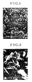
- crystalline products with angles means angular crystalline products, as opposed to spherical or ellipsoidal crystalline products or coalescent products of these, and includes those in which the angles possessed by the crystalline products in the protuberant portions in the surface of the electrodeposited chromium layer in electron-microscope photographs with magnifications of 3,000 to 30,000 are equal to or smaller than the angles, namely the face angles or radius of curvatures of edges, of the crystalline products as shown in Fig. 1 through Fig. 7.
- the portion of the protuberant crystalline products may have a projected area percentage preferably of 20% or more.
- the "projected area percentage" herein mentioned refers to that obtained by projection in the direction perpendicular to the support face having the electrodeposited layer of this invention, namely orthographic projection, and said area percentage is measurable by means of microscopic photography, etc.
- the constitutional ratio of the respective atoms such as oxygen, chromium and iron may be varied from the surface of the electrodeposited chromium layer toward the substrate (iron material); for example the number of oxygen atoms, without increasing, or after slightly increasing, soon begin to decrease; chromium atoms, after being increasing, gradually decrease on nearing the substrate; and the atoms constituting the substrate such as iron begin to appear at a certain depth from the surface of the electrodeposited chromium layer, and increase in number as the depth increases.
- the electrodeposited chromium layer is constituted on the substrate side substantially of the atoms constituting the substrate and chromium atoms, and the constitutional ratios vary continuously such that the ratio of the atoms constituting the substrate becomes greater and the ratio of chromium smaller on nearing said substrate.
- the electrodeposited chromium layer refers to a region from the support surface to a position at which the number of the atoms constituting the substrate and the number of chromium atoms are identical, its thickness is preferably 0.01 to 10 um, particularly preferably 0.01 to 4 Ilm.
- the thickness can be determined by fluorescent X-ray analysis as an average value by a quantitative determination with reference to the calibration curve previously prepared from standard chromium plated layers with known thicknesses.
- the electrodeposited chromium layer is constituted on the substrate side substantially of the atoms constituting the substrate and chromium atoms" means that the sum of the respective atomic concentrations of the atoms constituting the substrate and chromium atoms is 60% or more.
- the surface side portion of the electrodeposited chromium layer refers to the portion from the surface of said electrodeposited layer to the position where the atomic concentration of the atoms constituting the substrate exceeds 20%.
- the sum of the respective atomic concentrations of chromium atoms and oxygen atoms is 50% or more, thus meaning that other components, for example carbon atoms, chlorine atoms, sulfur atoms, calcium atoms, nitrogen atoms and fluorine atoms may be present in an amount which does not impair the effect of this invention.
- the above atomic concentrations can be determined by the surface analytical means such as photoelectric spectroscopy (e.g. X-ray photoelectric spectroscopy), and Auger electron spectroscopy.
- photoelectric spectroscopy e.g. X-ray photoelectric spectroscopy
- Auger electron spectroscopy e.g. Auger electron spectroscopy
- the profile of the elements in the direction of depth of the electrodeposited chromium layer in the support in this invention may be determined by Auger electron spectroscopy, and the atomic concentrations at various depths at various portions of the electrodeposited chromium layer can be determined by local analyses by means of the Scanning Auger Microprobe (e.g., PHI. Model 595, 600 produced by Perkin Elmer Co.).
- Scanning Auger Microprobe e.g., PHI. Model 595, 600 produced by Perkin Elmer Co.
- the above depths from the surface can be determined by transformation based on the depth direction analyses as described below.
- the depth direction analyses can be measured by means of the aforesaid PHI Model 595, argon ion being used as the ion gun and etching effected at a speed of 20 A/min with thallium oxide (Ta 2 0 5 ) as the standard (determined from the time for etching of Ta 2 0 5 with known film thicknesses); in calculation of the elemental composition, the peak intensities of the Auger spectrum (differential form) employed concern the peak at 529 eV for chromium and the peak at 503 eV for oxygen, the relative sensitivities of chromium and oxygen employed being the values as disclosed in L. E. Davis, P. W. Palberg, E. G. Riach, R. E. Weber, N.
- the diameter of the primary electron beam was narrowed to 500 A to 1 Ilm to analyze the crystalline portion and the non-crystalline portion separately for micro-regional analysis.
- the primary electron beam is irradiated accurately onto the central portion of the crystalline portion so that the brim of the crystalline portion may not be included within the irradiation region of said beam. For example, with respect to the plate crystal portion, irradiation is effected at the center of said flat plate portion.
- the ion beam for etching is irradiated at an incident angle of 45° to 90° relative to the crystalline portion plane and the non-crystalline portion plane.
- the incidence of said ion beam onto the spot to be analyzed should not be interfered by other surrounding crystals not to be analyzed.
- the primary electron gun and the electron energy analyzer are arranged around the same directional axis (co-axial type) for the present measurement.
- the depth Xnm from the surface as defined above is obtained by transforming the etching time from the aforesaid etching speed into depth, being calculated on the basis that all the compositions are chromium oxide (Cr 2 0 3 ). Further, the aforesaid elemental composition shows the ratio of number of atoms per unit area.
- the elemental composition in the surface side portion of the electrodeposited chromium layer consists substantially of chromium and oxygen and the respective elemental compositions of chromium and oxygen at said portion are substantially even at the same depth from said surface and at respective portions on said surface.
- the respective elemental compositions of chromium and oxygen anywhere irrespective of whether at the portion of the protuberant crystalline products on the surface or at any other portion, are substantially the same.
- the wording "substantially the same” means that, in the element profile in the depth direction at each portion, the value of Xo is within the range of error of ⁇ 80%. The above error is calculated by dividing the difference between the two values by the greater value of the two values and multiplying the resultant value by 100.
- the surface side portion of the electrodeposited chromium layer of this invention may be judged by the elemental analysis in the depth direction to consist substantially of chromium oxides (including also hydrates) and metallic chromium, with the ratio of metallic chromium increasing with increasing depth.
- chromium oxides there may be included oxides of divalent, trivalent or hexavalent chromium, primarily trivalent chromium oxides.
- Fig. 1 through Fig. 7 show the photographs of the electrodeposited chromium layer surfaces of the typical supports for lithographic printing plate of this invention taken with a scanning type electron microscope, Fig. 1 through Fig. 5 show various plate crystals, while Fig. 6 and Fig. 7 show cubic crystals and agglomerated product of cubic crystals.
- the Electrolyte 1 as shown in Table 1 and an iron plate as the counter-cathode may be employed, and electrolytic treatment is typically carried out under the Electrolysis Conditions 1 as shown in Table 2.
- the thus pre-treated iron was washed with water by spraying and then transferred to the main treatment step.
- This main treatment step is a step for forming the electrodeposited chromium layer of this invention, in which Electrolyte 2 as shown in Table 3 is cooled or heated by a coil tube for temperature control to adjust the liquid temperature, and electrolytic treatment is typically conducted under the Electrolysis Conditions 2 as shown in Table 4.
- the support can be treated at a suitable temperature by washing with or dipping in an aqueous hydrophilic resin solution such as aqueous carboxymethylcellulose solution, aqueous polyvinyl alcohol solution, polymethacylic acid solution, polyacrylic acid solution or aqueous sodium alginate solution; an aqueous acidic solution such as phosphoric acid or aluminum sulfate, an alkali such as caustic soda, or a fluoride such as potassium fluorozirconate or potassium fluorotitanate or aqueous solutions of salts containing group 5, 6 metals such as ammonium molybdenate, phosphotungustic acid, sodium phosphotungstate, sodium phosphomolybdenate or silicotungstic acid.
- an aqueous hydrophilic resin solution such as aqueous carboxymethylcellulose solution, aqueous polyvinyl alcohol solution, polymethacylic acid solution, polyacrylic acid solution or aqueous sodium alginate solution
- the support of this invention on account of the surface shape formed by the electrodeposited chromium layer, possesses excellent adhesion to layers comprising polymeric compounds having lipophilic surfaces such as photosensitive layers provided thereon, and when employed for a photosensitive lithographic printing plate, the plate has good printing life. Also, due to wide tolerance in developing methods, the loss of image portions is very small even by the "hand processing" which requires overly frictional treatment.
- the support of this invention gives the advantages of high production efficiency and low production cost because of simple production steps.
- Photosensitive lithographic printing plates can be produced by coating photosensitive compositions, for example, with the use of organic solvents, on the support of this invention.
- Photosensitive compositions contain as essential components photosensitive substances.
- the photosensitive substance there may be employed a substance which can be exposed to light to vary the solubility of the photosensitive composition layer relative to the developer, to vary the adhesive force between molecules, or to vary the affinity of the photosensitive composition layer for water and oil.
- posi-type photosensitive substances of the quinoneazide type such as o-naphthoquinonediazide compounds well known in the art.
- o-Quinonediazide compounds are compounds having at least one o-quinonediazide group, preferably o-benzoquinodiazide group or o-naphthoquinonediazide group, and include compounds of various known structures, as described in detail in J. Kosar "Light-Sensitive Systems” (published by John Wiley & Sons, Inc., 1965), pp. 339-353.
- esters of various hydroxyl compounds with o-naphthoquinonediazide sulfonic acid are preferred.
- preferable hydroxyl compounds there may be included condensed resins of phenols with carbonyl containing compounds, especially resins obtained by condensation in the presence of an acidic catalyst.
- Said phenols may include phenol, resorcin, cresol and pyrogallol, while said carbonyl containing compounds may include aldehydes, such as formaldehyde and benzaldehyde, and ketones such as acetone.
- phenol-formaldehyde resins cresol-formaldehyde resins, pyrogallol-acetone resins and resorcin-benzaldehyde resins are preferred.
- o-quinonediazide compounds include esters of benzoquinone - (1,2) - diazidesulfonyl chloride or naphthoquinone - (1,2) - diazidesulfonyl chloride with phenol-formaldehyde resins; sulfonic acid esters of naphthoquinone - (1,2) - diazidesulfonyl chloride and pyrogallolacetone resins as disclosed in U.S.
- Patent 3,635,709 condensed products of naphthoquinone - (1,2) - diazide - (2) - 5 - sulfonyl chloride and resorcinol-benzaldehyde resins as disclosed in Japanese Unexamined Patent Publication No. 1044/1981; ester compounds of naphthoquinone - (1,2) - diazide - (2) - 5 - sulfonyl chloride and resorcinol-pyrogallol-acetone co-condensed products as ' disciosed in Japanese Unexamined Patent Publication No.
- o-quinonediazide compounds include those obtained by the esterification reaction of o-naphthoquinonediazidesulfonyl chloride with polyesters having terminal hydroxyl groups as disclosed in Japanese Unexamined Patent Publication No. 117503/1975 and those obtained by the esterification reaction of o-naphthoquinonediazidesulfonyl chloride with p-hydroxylstyrene homopolymers or copolymers of p-hydroxylstyrene with other copolymerizable monomers.
- o-quinonediazide compounds are contained preferably in amounts of 5 to 80% by weight, particularly preferably 10 to 50% by weight, based on the total solids of the photosensitive composition.
- Such a quinonediazide type posi-type photosensitive metal preferably may be used in combination with an alkali-soluble resin as binder.
- alkali-soluble resins preferred are those obtained by reacting phenols with ketones or aldehydes in the presence of an acidic catalyst.
- Said phenols include, for example, phenol, cresol and p-substituted phenols.
- Said aldehydes include, for example, acetaldehyde and formaldehyde, preferably formaldehyde.
- ketones acetone is preferred.
- alkali-soluble resins there may be mentioned, for example, phenol-formaldehyde resins, cresol-formaldehyde resins, phenol-cresol-formaldehyde co-condensed resins as disclosed in Japanese Unexamined Patent Publication No. 57841/1980, co-condensed resins of p-substituted phenol, phenol or cresol and formaldehyde as disclosed in Japanese Unexamined Patent Publication No.
- alkali-soluble resins are contained preferably in amounts of 30 to 90% by weight, particularly 50 to 85% by weight, based on the total solids in the photosensitive composition.
- diazo resins typically condensed products of aromatic diazonium salts and formaldehyde.
- Particularly preferred are salts of condensed products of p-diazodiphenylamine and formaldehyde or acetaldehyde, diazo resin inorganic salts which are the reaction products of hexafluorophosphates, tetrafluoroborates, perchlorates or periodates with said condensed products and diazo resin organic salts of said condensed products with sulfonic acids as disclosed in U.S. Patent 3,300,309. Further, diazo resins are used preferably together with binders.
- binders there may be employed various polymeric compounds, preferably copolymers of monomers having aromatic hydroxyl groups such as N - (4 - hydroxyphenyl)acrylamide, N - (4 - hydroxyphenyl)methacrylamide, o-, m-, or p-hydroxystyrene, o-, m- or p-hydroxyphenyl methacrylate, etc. with other monomers as disclosed in Japanese Unexamined Patent Publication No. 98613/1979; polymers containing hydroxyethyl acrylate units or hydroxyethyl methacrylate units as primary recurring units as disclosed in U.S.
- Patent 4,123,276 natural resins such as shellac, and rosin; polyvinyl alcohol; polyamide resins as disclosed in U.S. Patent 3,751,257; linear polyurethane resins as disclosed in U.S. Patent 3,660,097; phthalated resins of polyvinyl alcohol; epoxy resins condensed from bisphenol A and epichlorohydrin; and celluloses such as cellulose acetate and cellulose acetate phthalate.
- photosensitive polymers such as polyesters, polyamides or polycarbonates including as photosensitive groups in the polymeric main chain or side chain.
- photosensitive polyesters obtained by condensation of phenylenediethyl acrylate, hydrogenated bisphenol A and triethyleneglycol as disclosed in Japanese Unexamined Patent Publication No. 40415/1980; and photosensitive polyester compounds derived from (2 - propenylidene)malonic acid compounds such as cinnamilidene malonic acid and bifunctional glycols as disclosed in U.S. Patent 2,956,878.
- aromatic azide compounds having azide groups bonded directly or through carbonyl group or sulfonyl group to aromatic rings.
- aromatic azide compounds having azide groups bonded directly or through carbonyl group or sulfonyl group to aromatic rings.
- polyazidestyrene, polyvinyl - p - azidebenzoate, polyvinyl - p - azidebenzal as disclosed in U.S. Patent 3,096,311; the reaction products of azidearylsulfanyl chloride and unsaturated hydrocarbon type polymers as disclosed in Japanese Patent Publication No. 9613/1970; and polymers having sulfonylazide or carbonylazide as disclosed in Japanese Patent Publication Nos. 21067/1968, 229/1969, 22954/1969 and 24915/1970.
- photosensitive substance there may also be employed a photopolymerizable composition comprising an addition polymerizable unsaturated compound.
- the support of this invention can be used as a support of a lithographic printing plate obtained by electrophotographic process.
- the lithographic printing plate obtained by the method (1) comprises a support of this invention having a photoconductive layer on the total surface thereof and having a toner-image only at the image portions on said photoconductive layer.
- the lithographic printing plate obtained by the method (2) comprises a support of this invention having a photoconductive layer only at an image portion thereon and having a toner-image on the entire surface of said photoconductive layer.
- the lithographic printing plate obtained by the method (3) comprises a support of this invention having a polymeric layer only at an image portion thereon and having a toner-image on the total surface of said polymeric layer.
- the photoconductive layer mentioned above comprises a photoconductive material.
- the photoconductive material may be, for example, an inorganic or organic photoconductive material or a photoconductive organic pigment. At least one of them is used.
- the inorganic photoconductive material may be, for example, a selenium- or zinc oxide-based material or cadmium sulfide which are known for electrophotography.
- the organic photoconductive material may be, e.g. polyvinylcarbazole, oxazoles or pyrylium salt. Examples of the photoconductive organic pigments are phthalocyanine and quinacridone pigments.
- the aforesaid photoconductive material (and sensitizing agent) can be dissolved or suspended in a solution containing at least one natural or synthetic high-molecular substance (e.g. styrene, silicone or phenol resin), coated onto a support and dried according to a known procedure.
- the photoconductive layer may also contain various additives, for example, surface active agents for improving the coating property, and plasticizers for imparting softness and wear resistance to the coated layer.
- an intermediate layer e.g. of polyvinyl alcohol, ethyl cellulose or polyacrylic acid
- the thickness of the photoconductive layer after drying is preferably 1 ⁇ to 50 u, and more preferably 1 p to 15 p.
- the thus obtained printing plate material is then electrostatically charged by the usual electrophotography, and exposed to the xenon, halogen, fluorescent, or tungsten-filament lamp or to a laser beam such as semiconductor, Ar + or He-Ne laser, thereby to form an electrostatic latent image.
- the formed latent image is then toner-developed.
- the toner-image can be, after toner-developing, fixed with heat by use of a heat plate, heat roller or heat rays, for example. Then, in the non-imaged area (where there is no toner attached), the photoconductive layer is made hydrophilic in the method (1) or removed by use of an appropriate solvent in the method (2) to give a lithographic printing plate.
- a support of this invention is not essential to use a support of a photoconductive layer.
- the toner-image is transferred onto a polymeric layer which a support of this invention has thereon and the transferred toner-image is fixed with heat. Then the polymeric layer in the non-imaged area is removed to give a lithographic printing plate.
- toner development it is possible to use a dry process in which both toner and carrier are solid, a wet process in which the toner or the carrier is liquid, or an aerosol process in which a gas flow is used as the carrier regardless of whether the toner is solid or liquid.
- the toner is hydrophobic and has an ink accepting property.
- the toner may have positive or negative polarity.
- the support of this invention can be used as a support of a lithographic printing plate obtained by the use of a silver halide emulsion.
- a support of this invention is used as a support of a physical development nuclei-containing layer.
- This silver halide emulsion layer may be carried on the support having the physical development nuclei layer or a separate support.
- the silver complex may be produced in an exposed area or non-exposed area. A method producing it in a non-exposed area is described in detail in, for example, United States Patent Nos. 3083097 and 3161508, Japanese Patent Publication Nos. 26526/1971, 16725/1973, and 30562/1973.
- the method producing a silver complex in an exposed area comprises exposing an element comprising a support carrying silver halide particles, non-photosensitive metal salt particles being more soluble than the silver halide particles and the surface portion thereof being made less soluble and physical development nuclei, and treating the exposed element with a treating solution containing a material capable of solving said metal salt particles, and is described in detail, for example, in Japanese Unexamined Patent Publication Nos. 48554/1979, 165140/1981, 44138/1982 and 44153/1982.
- the support of this invention can be used as a support of a lithographic printing plate requiring no damping water.
- the lithographic printing plate material giving the printing plate comprises a support of this invention having an ink-repelling layer thereon.
- the ink-repelling layer becomes reactive on light exposure, it does not require a layer other than the ink-repelling layer. In case the ink-repelling layer does not become reactive on light exposure, it requires a light sensitive layer other than the ink-repelling layer.
- a usable photosensitive substance may be any known one for such a printing plate, e.g., a diazonium salt such as a formaldehyde condensate of p-diazodiphenylamine salt, an o-naphthoquinonediazide compound, a photopolymerizable photosensitive material having an ethylenically unsaturated group, an azide compound, an ⁇ , ⁇ -unsaturated ketone compound or an a-phenylmaleimide compound, or a compound obtained by reacting the above-listed photosensitive materials and silicone compounds.
- a diazonium salt such as a formaldehyde condensate of p-diazodiphenylamine salt, an o-naphthoquinonediazide compound, a photopolymerizable photosensitive material having an ethylenically unsaturated group, an azide compound, an ⁇ , ⁇ -unsaturated ketone compound or an a-phen
- the aforesaid ink-repelling layer may be formed by use of diorganopolysiloxane compounds such as dimethylpolysiloxane and diphenylpolysiloxane, copolymers of these compounds or poly-fluorinated compounds.
- the ink-repelling layer which becomes reactive on light exposure may be formed by use of organopolysiloxane or poly-fluorinated compound, for example, each having a photosensitive group.
- the lithographic printing plate material described above is exposed through a positive or negative film to an active light beam emitted from a mercury vapor, a carbon arc or a metal halide lamp, for example.
- the exposed printing plate material is then developed with a developing solution suitable for the photosensitive substance to complete the printing plate.
- the thus obtained printing plate is then used for printing with a printing press which is not equipped with damping water feeder.
- the support of this invention can be used as a support of a duplicate plate obtained by a method such as printing on a support of a duplicate plate from an original printing plate using a material such as an ink which can be hardened and becomes ink-receptive after hardening the material on the support of the duplicate plate.
- Electrolysis treatment was applied, using the Electrolyte I as shown in Table 5 and an iron plate as the counter-electrode, under the Electrolysis Conditions I as shown in Table 6.
- the thus pre-treated iron was washed with water by spraying and then transferred to the main treatment step.
- the Electrolyte II and the Electrolysis Conditions II in the main treatment step are shown in Table 7 and Table 8.
- the carbon steel plate having thus finished the main treatment step was subsequently subjected to shower washing with water and transferred to the post-treatment step.
- the plate was dipped first in an aqueous 5% caustic soda solution at 40°C for one minute, followed by shower washing with water, then dipped in an aqueous carboxymethylcellulose sodium salt solution (0.07% by weight) at room temperature for one minute, followed by shower washing with water.
- the product was dried on cool air.
- Measuring conditions were; ion gun:4 KeV, 25 mA, raster 5 mmx5 mm; argon ion employed, etching speed of 20 ⁇ lmin with Ta 2 0 5 as the standard; primary electron gun: 10 KeV; diameter of electron beam narrowed to about 500 A.
- the electron beam was irradiated on the center of the flat portion of the plate crystal as in Figs.
- the peak intensities of Auger spectrum were those of the peak at 529 eV for chromium and the peak at 503 eV for oxygen, with the relative sensitivity of chromium being made 0.28 and that of oxygen 0.35.
- the depths from the surface on the axes of abscissa in Figs. 8 and 9 are transformations of the etching time from said etching speed into depths, being calculated by regarding all the compositions as Cr z 0 3 .
- Fig. 10 shows the results of analysis obtained by etching the substrate at the portion where no crystal protrudes.
- the measuring conditions were the same same as above except that the etching speed was made 85 A/min (Ta 2 0 5 as the standard).
- the axis of abscissa in Fig. 10 is the transformation of etching time into depth as mentioned above, being calculated by regarding all the compositions as chromic oxide (Cr 2 0 3 ).
- the crystal portion was also similarly subjected to etching to the substrate of iron, whereby the profile of elements in the depth direction was obtained similarly as in Fig. 10.
- the composition is constituted substantially of iron atoms and chromium atoms in the substrate side, with the composition being continuously varied such that the constitutional ratio of iron is greater and that of chromium atoms smaller as nearer to said substrate.
- a photosensitive coating solution having the following composition by a rotary coating machine, followed by drying at 100°C for 4 minutes, to obtain a lithographic printing plate material.
- the weight of the coating after drying was about 2.7 g/m 2 .
- lithographic printing plate material were closely contacted a posi-manuscriptfilm and the Step Tablet for measurement of sensitivity (produced by Eastman Kodak Co., No. 2, 21 steps with density differences each of 0.15), and light exposure was applied by a 2 KW metal halide lamp (ldolfin 2000 produced by Iwasaki Denki Co., Ltd.) as the light source from a distance of 1 m for 80 seconds, followed by development with an aqueous 4% sodium metasilicate solution at 25°C for 45 seconds to obtain a lithographic printing plate.
- a 2 KW metal halide lamp ladolfin 2000 produced by Iwasaki Denki Co., Ltd.
- treating chemicals resistance test and printing test were conducted.
- durability to aqueous isopropyl alcohol solution used in Darlgrain damping water system was examined.
- the printing plate having formed an image with density differences on the steps of the above gray scale was immersed in an aqueous 35% isopropyl alcohol solution at room temperature for 20 minutes and washed with water; and then the image portion was rubbed with a defatted cotton impregnated with water.
- the extent of corrosion to the chemical of the image portion was judged.
- the aforesaid printing plate was free from corrosion to exhibit good resistance to the treating chemicals.
- Printing resistance test was conducted by carrying out printing with the printing plate mounted on an offset printing machine (Hamadastar 900 CDX), and evaluated by the number of printed sheets obtained until there are formed damages on the image portion to make printing no longer possible. As the result, with the use of the aforesaid printing plate, good printing products were obtained up to 200,000 sheets.
- a support for lithographic printing plate having provided an electrodeposited chromium layer on a carbon steel was produced according to the method as described in European Patent Publication No. 020021. That is, the same kind of carbon steel plate as in Example 1 was immersed in a pre-washing tank (dil. hydrochloric acid) at 40°C for 30 seconds, washed with water and then immersed in a pulverization tank containing 60 g of ammonium hydrogen fluoride per one liter of water at 40°C for 5 minutes, followed by washing with water.
- a pre-washing tank diil. hydrochloric acid
- the resultant treated plate was immersed in a plating bath containing 250 g of chromic acid anhydride and 2 g of sulfuric acid per one liter of water, connected to the cathode and plating treatment was carried out at a bath temperature of 35°C, a current density of 110 A/dm 2 for 60 seconds.
- a plating bath containing 250 g of chromic acid anhydride and 2 g of sulfuric acid per one liter of water
- Example 2 Light exposure and development were applied on such a lithographic printing plate material in the same manner as described in Example 1 to obtain a lithographic printing plate, which was in turn subjected to the same treating chemicals resistance test and printing test as in the above Example 1. It was found that this printing plate had poor treating chemicals resistance with corrosion being markedly observed at the image portion. Also, when about 50,000 sheets were printed, ink spreading at the dots portion and scumming at the non-image portion occurred, which could not be repaired to make further printing possible.
- a steel plate with a thickness of 0.1 mm was subjected to the electrolytic treatment of pre-treatment similarly as in Example 1.
- the steel plate having been subjected to the pre-treatment step was subjected to shower washing with water and the subsequent main treatment step was applied.
- the composition of the Electrolyte II and the Electrolytic Conditions II in the main treatment step are shown in Table 9 and Table 10.
- the steel plate was then washed by showering with water and dried on air at room temperature.
- a photosensitive coating solution having the composition shown below by use of a rotary coating machine, followed by drying at 85°C for 3 minutes, to obtain a lithographic printing plate material.
- the diazo resin B is a hexafluorophosphoric acid salt obtained by mixing an aqueous 5% diazo resin (trade name: D-012 produced by E.H.C.
- the above copolymer had a weight average molecular weight of 80,000, further the molecular weight distribution of the above resin was measured by gel permeation chromatography (GPC) to find that the fractions with molecular weights of trimer or lower comprise 93% of the total fractions.
- the weight of the coating after drying was 2.0 g/m 2 .
- lithographic printing plate material was closely contacted with a negative manuscript film and light exposure was applied thereon at a distance of 1 m from a 2 KW metal halide lamp (Idolphin 2000, produced by Iwasaki Denki Co., Ltd.) as the light source, followed by development with a developer having the following composition, to obtain a lithographic printing plate.
- a 2 KW metal halide lamp (Idolphin 2000, produced by Iwasaki Denki Co., Ltd.) as the light source
- the developing conditions were 25°C and 45 seconds.
- Hand processing was carried out by impregnating a sponge sufficiently with the above developer, rubbing uniformly and lightly the surface of the above lithographic printing plate material after exposure with the sponge for 2 minutes, followed by washing with water.
- the above lithographic printing plate material was not damaged at the image portion at all either by the hand processing or by the developing machine.
- Printing test were performed as in Example 1. As a result, the lithographic printing plate using the support of this invention gave good printed products up to 200,000 sheets.
- the following sample was prepared for a comparative test. That is, there was prepared a plate material having provided an electrodeposited chromium layer in the same manner as in Comparative Example 1 on the same steel plate as used in Example 2, and on this steel plate support was coated and dried the same photosensitive coating solution as described in Example 2 to provide a lithographic printing plate material. Then, a lithographic printing plate was prepared from this material and printing life test was conducted. As a result, in the hand processing, the image portion was markedly damaged until it was almost peeled off. Further, in printing, a part of the image portion peeled off when 80,000 sheets had been printed and printing was no longer possible.
- the electrolytic treatment of the pre-treatment step was applied as the pre-treatment step similarly as in Example 1.
- the iron plate was then washed by showering with water and then subjected to the subsequent main treatment.
- the composition of the Electrolyte II and the Electrolysis Conditions II in the main treatment are shown in Table 11 and Table 12.
- the iron plate was subsequently subjected to shower washing with water, and thereafter trasnferred to the post-treatment step.
- the plate was first immersed in an aqueous 5% caustic soda solution at 40°C for one minute, followed by shower washing with water, and then immersed in an aqueous solution (1 wt.%) of potassium fluorozirconate at room temperature for about one minute, followed by shower washing with water.
- the iron plate was then dried in cool air.
- the weight of the coating after drying was about 2.5 g/m 2 .
- lithographic printing plate material was closely contacted with a Step Tablet for measurement of sensitivity (produced by Eastman Kodak Co., No. 2, 21 steps with density differences each of 0.15) and a posi manuscript film, and light exposure was applied by a 2 KW metal halide lamp (ldolfin 2000 produced by Iwasaki Denki Co., Ltd.) as the light source from a distance of 1 m for 80 seconds, followed by development with an aqueous 4% sodium metasilicate solution at 25°C for 45 seconds to obtain a lithographic printing plate.
- a 2 KW metal halide lamp ladolfin 2000 produced by Iwasaki Denki Co., Ltd.
- the treating chemicals resistance test and printing test were conducted.
- the durability to Ultra Plate Cleaner (produced by A.B. Chemical Co.) which is used as the washing liquid for removal of the scumming generated at the non-image portion during printing was examined.
- the printing plate having formed an image with density differences on the steps of the above gray scale was immersed in the stock solution of Ultra Plate Cleaner at room temperature for 20 minutes and washed with water. By comparison of the resultant image portion with the image portion before immersion, the extent of corrosion to the chemicals of the image portion was judged. It was found that the aforesaid printing plate was free from corrosion and also, with respect to the dots, the dots of an area percentage of 2% were maintained, thus exhibiting good resistance to the treating chemicals.
- the printing life test was conducted as in Example 1. With the use of the aforesaid printing plate, good printing products were obtained for up to 250,000 sheets. This printing plate had good water retentivity and printing could easily be managed.
- the following sample was prepared for comparative purposes. That is, there was prepared a plate material having provided an electrodeposited chromium layer in the same manner as in Comparative Example 1 on the same iron plate as used in Example 3, and on this iron plate support was coated and dried the same photosensitive coating solution as described in Example 3 to provide a lithographic printing plate material. Then, a lithographic printing plate was prepared from this material as in Example 3, and the treating chemicals resistance test and printing life test were conducted. It was found that the treating chemicals resistance was poor with the image portion being substantially lost with Ultra Plate Cleaner and all the dots to an area percentage of 5% were lost. In printing, a part of the image portion peeled off when 60,000 sheets had been printed and printing was no longer possible.
- composition was dispersed and homogenized in a ball mill at normal temperature for 48 hours:
- the obtained coating composition was applied onto the support used in Example 1 to a thickness of 10 ⁇ after drying.
- the thus formed printing plate material was then negatively charged using corona discharge equipment, and exposed imagewise to a light source consisting of ten 20 W fluorescent lamps through a lens system by use of a reflection positive original.
- the electrostatic latent image thus formed was then toner-developed using a polystyrene-based toner and by the magnet brush process.
- the resulting toner image was then fixed with heat, and subjected to hydrophilicity-imparting treatment to form a printing plate. When used for printing with an offset press, this printing plate yielded 300,000 satisfactory prints having a sharp image.
- composition was dispersed and homogenized in a ball mill at normal temperature for 48 hours.
- the obtained coating composition was applied onto the support used in Example 2 to a thickness of 5 p after drying. After being charged, exposed, toner-developed and fixed with heat as described in Example 4, this plate was dipped in an aqueous alkali solution containing sodium silicate and sodium hydroxide to dissolve and remove the photoconductive layer in the non-image area (where the toner is not attached). When used for printing with an offset press, the thus obtained printing plate yielded 300,000 satisfactory prints having a sharp image.
- the above composition was dispersed with ultrasonic dispersing equipment at normal temperature for 5 minutes, and used to make a printing plate material as described in Example 5.
- the plate material was then treated in the same way as in Example 5 to form a printing plate.
- the printing life of this printing plate was 300,000 prints or more.
- Example 6 The printing plate material obtained in Example 6 was positively charged using corona discharge equipment. An image was photographed at an enlarging factor of 16 (area ratio) from a micro film original and a commercially available photographic enlarger, and then developed using a + liquid developer. This was followed by the same treatment as that described in Example 5 to obtain a printing plate exhibiting a sharp image.
- Example 6 The printing plate material obtained in Example 6 was treated to form a printing plate in the same way as described in Example 7, except that a He-Ne laser was used as the light source. In this way, a printing plate exhibiting a sharp image was obtained.
- the following coating composition was applied on the support used in Example 1 to a thickness of 3 p after drying to obtain a printing plate material comprising the support having a polymeric layer thereon.
- a photosensitive material using commercial zinc oxide was negatively charged using corona discharge equipment, and exposed imagewise to a light source consisting of ten 20 W fluorescent lamps through a lens system by use of a reflection positive original.
- the electrostatic latent image thus formed was then toner-developed using a polystyrene-based toner and by the magnet brush process.
- the resulting toner image was then transferred onto the polymeric layer.
- the toner-image on the polymeric layer was fixed with heat.
- the polymeric layer in non-image area was removed with methylcellosolve.
- the printing plate thus obtained was used for printing with an offset press; this printing plate yielded 200,000 satisfactory prints having a sharp image.
- a colloid solution prepared as described below was uniformly applied as a physical development nucleus onto the support made as described in Example 1, and dried to prepare a printing plate material.
- Liquids A and 8 were mixed with violent stirring at room temperature, liquid C added and stirred for 5 minutes, and cooled to prepare a palladium sulfide physical development nucleus. Appropriate amounts of saponin as a surface active agent and formalin as hardening agent were then added, respectively, and the obtained mixture was applied onto the support to a wet thickness of 30 P .
- a photosensitive material was prepared by applying a high contrast silver chloride bromide emulsion, which was prepared according to a usual procedure, onto a photographic polyester film, followed by drying. The thus prepared photosensitive material was then used to photograph a positive original by use of a process camera. The photosensitive element exposed in this way was then contacted with the physical development nucleus layer, and developed for 60 seconds by use of the developing solution having the following composition:
- a negative printing plate material was made by the diffusion-transfer process as described below by using the support obtained in the same way as in Example 2.
- a silver iodide bromide emulsion (silver iodide: 5 mol %) was prepared from silver nitrate, potassium bromide and potassium iodide. The emulsion was then chemically sensitized with gold-sulfur sensitizier. Then, 0.3 g of 4 - hydroxy - 6 - methyl - 1,3,3a,7 - tetrazaindene per mol of silver halide was added as a stabilizer to the chemically sensitized emulsion to prepare a silver iodide bromide emulsion having a moderate sensitivity.
- a pure silver chloride emulsion was prepared from silver nitrate and sodium chloride, and cleaned by sedimentation. Then, 0.6 g of 1 - phenyl - 5 - mercaptotetrazole per mol of silver chloride was added to the emulsion to make it sparingly soluble.
- the previously prepared photosensitive silver halide emulsion (a) was mixed with the thus prepared sparingly-soluble pure silver chloride emulsion (b). After adding an appropriate amount of saponin as a surface active agent to the obtained mixture, the mixture was applied onto the aforesaid physical development nucleus layer used in Example 10 to prepare a printing plate material.
- Both emulsions (a) and (b) were mixed together in a proportion of 0.2 mol of silver iodide bromide emulsion per mol of silver chloride emulsion on the silver basis.
- a negagive original film was brought into close contact with the silver halide emulsion layer, exposed and developed with a developing solution having the composition described below at a temperature of 30°C for 90 seconds. Then, the printing plate material was dipped in running water at a temperature of 20°C for 30 seconds to remove the upper silver halide layer.
- the obtained printing plate was treated to impart ink receptivity as described in Example 10, and then immediately used for printing with an ink.
- the results were as shown below.
- the printing press used was Toko Model 810.
- the values in the "prints before stains disappear" column were determined by supplying an excess of the ink so that the whole surface of the printing plate was inked, stopping the supply of ink, and printing until the stains disappeared).
- the photopolymerizable composition having the composition described below was whirl-coated onto the support obtained in accordance with Example 1, and dried at a temperature of 50°C for 10 minutes.
- the silicone layer had a thickness of 6 ⁇ in dry state.
- the thus obtained printing plate was set on an offset press (Komori Sprint L-25B) and used for printing by using the coated paper, a dry offset color printing ink (Bowers available from Printing Ink Company) and by removing the damping water feeder. Thus, 150,000 high-quality prints were obtained.
- a printing plate material was made in the same way as described in Example 12, except that an electrochemically grained and anodized aluminium plate was used instead of the support in Example 1.
- this printing plate was used for printing in the same manner as Example 12, the silicone rubber at the non-image area peeled off from the substrate and caused the surface of the support to be scummed after 50,000 prints were produced.
- the photosensitive solution having the composition described below was wire bar coated onto the support obtained in accordance with the procedure described in Example 2, and dried at a temperature of 100°C for 3 minutes.
- the thickness of the obtained layer was 8 11. Then, the silicone rubber solution set forth below was wire bar coated onto the thus obtained photosensitive layer, and dried at a temperature of 50°C for 3 minutes.
- the thickness of the obtained silicone rubber layer was 2 ⁇ .
- the surface of the thus formed silicone rubber layer was laminated with a 6 p-thick polyethylene terephthalate film (Lumilar available from Toray Industries Inc. in Japan) to obtain a photosensitive lithographic printing plate material.
- a support was made according to the procedure in Example 1.
- the obtained support was set at the printing section of the automatic proof machine KF-122-E available from Dainippon Screen Mfg. Co., Ltd.
- An original plate which was made by exposing through a 150-line dot image original on the Sakura PS off-set plate SMP (available from Konishiroku Photo Industry Co., Ltd.), developed and processed, was used. In this way, the image was transferred to the support by printing.
- the transfer ink was an ultraviolet-curing ink (Dye Cure available from Dainippon Ink And Chemicals, Incorporated). After the transfer, the support was subjected to the exposure curing treatment by use of a 2 kW high-pressure mercury vapor lamp at a distance of 60 cm to obtain a duplicate printing plate.
- a duplicate printing plate was made in the same way as described in Example 14, except that a conventional chromium-plated iron plate (Tin Free available from Nippon Steel Corporation) was used instead of the support of this invention.
- this chromium-plated iron plate was not sufficiently clean, it was degreased in advance in an aqueous 5% sodium metasilicate solution at a temperature of 40°C for 4 minutes, followed by washing with water and drying. The iron plate was then dipped in an aqueous potassium permanganate solution at room temperature for 1 minute and then in an aqueous 1 % oxalic acid solution at room temperature for 1 minute, followed by washing with water and drying. In this way, the iron plate was cleaned, activated and then used for making the duplicate printing plate.
- Example 14 Up to the step for making the duplicate printing plate, no significant difference was observed compared with Example 14. However, in the printing with this printing plate, the non-image area scummed immediately after the printing was started, because of insufficient hydrophilicity and water receptive ability of the printing plate. In addition, after about 1,500 prints were produced, the image area was damaged and ink receptivity deteriorated so that normal prints could not be obtained any more.
Landscapes
- Chemical & Material Sciences (AREA)
- Engineering & Computer Science (AREA)
- Chemical Kinetics & Catalysis (AREA)
- Electrochemistry (AREA)
- Materials Engineering (AREA)
- Metallurgy (AREA)
- Organic Chemistry (AREA)
- Printing Plates And Materials Therefor (AREA)
Claims (11)


Applications Claiming Priority (2)
| Application Number | Priority Date | Filing Date | Title |
|---|---|---|---|
| JP105724/82 | 1982-06-18 | ||
| JP10572482 | 1982-06-18 |
Publications (3)
| Publication Number | Publication Date |
|---|---|
| EP0097503A2 EP0097503A2 (de) | 1984-01-04 |
| EP0097503A3 EP0097503A3 (en) | 1984-02-29 |
| EP0097503B1 true EP0097503B1 (de) | 1988-08-17 |
Family
ID=14415258
Family Applications (1)
| Application Number | Title | Priority Date | Filing Date |
|---|---|---|---|
| EP83303514A Expired EP0097503B1 (de) | 1982-06-18 | 1983-06-17 | Verfahren zur Herstellung einer Flachdruckplatte |
Country Status (3)
| Country | Link |
|---|---|
| US (1) | US4492740A (de) |
| EP (1) | EP0097503B1 (de) |
| DE (1) | DE3377703D1 (de) |
Families Citing this family (11)
| Publication number | Priority date | Publication date | Assignee | Title |
|---|---|---|---|---|
| JPS5931192A (ja) * | 1982-06-30 | 1984-02-20 | Konishiroku Photo Ind Co Ltd | 平版印刷版用支持体 |
| DE3424528A1 (de) * | 1984-07-04 | 1986-01-09 | Hoechst Ag, 6230 Frankfurt | Verfahren zum gleichzeitigen aufrauhen und verchromen von stahlplatten als traeger fuer lithographische anwendungen |
| US4687729A (en) * | 1985-10-25 | 1987-08-18 | Minnesota Mining And Manufacturing Company | Lithographic plate |
| EP0239423B1 (de) * | 1986-03-28 | 1996-03-20 | Japan Synthetic Rubber Co., Ltd. | Positiv arbeitende photoempfindliche Kunststoffzusammensetzung |
| US5437952A (en) * | 1992-03-06 | 1995-08-01 | Konica Corporation | Lithographic photosensitive printing plate comprising a photoconductor and a naphtho-quinone diazide sulfonic acid ester of a phenol resin |
| US5816161A (en) * | 1994-07-22 | 1998-10-06 | Man Roland Druckmaschinen Ag | Erasable printing plate having a smooth pore free metallic surface |
| US5786090A (en) * | 1996-02-29 | 1998-07-28 | Flex Products, Inc. | Laser imageable thin film structure and printing plate incorporating the same |
| JP2000208431A (ja) * | 1999-01-13 | 2000-07-28 | Tadahiro Omi | 酸化クロム不働態膜が形成された金属材料及びその製造方法並びに接流体部品及び流体供給・排気システム |
| US7420163B2 (en) * | 2005-04-29 | 2008-09-02 | Revera Incorporated | Determining layer thickness using photoelectron spectroscopy |
| US7231324B2 (en) * | 2005-04-29 | 2007-06-12 | Revera Incorporated | Techniques for analyzing data generated by instruments |
| CN115787016B (zh) * | 2022-12-14 | 2024-11-26 | 上海天承化学有限公司 | 一种图形电镀工艺及印制线路板 |
Family Cites Families (4)
| Publication number | Priority date | Publication date | Assignee | Title |
|---|---|---|---|---|
| US2780592A (en) * | 1951-08-22 | 1957-02-05 | Bethlehem Steel Corp | Electrolytic treatment of metal surfaces |
| JPS5424352B2 (de) * | 1972-12-05 | 1979-08-20 | ||
| US4296182A (en) * | 1978-05-08 | 1981-10-20 | Toyo Seikan Kaisha Limited | Can composed of electrolytically chromated steel |
| US4371430A (en) * | 1979-04-27 | 1983-02-01 | Printing Developments, Inc. | Electrodeposition of chromium on metal base lithographic sheet |
-
1983
- 1983-06-10 US US06/503,186 patent/US4492740A/en not_active Expired - Fee Related
- 1983-06-17 EP EP83303514A patent/EP0097503B1/de not_active Expired
- 1983-06-17 DE DE8383303514T patent/DE3377703D1/de not_active Expired
Also Published As
| Publication number | Publication date |
|---|---|
| DE3377703D1 (en) | 1988-09-22 |
| EP0097503A3 (en) | 1984-02-29 |
| EP0097503A2 (de) | 1984-01-04 |
| US4492740A (en) | 1985-01-08 |
Similar Documents
| Publication | Publication Date | Title |
|---|---|---|
| US3511661A (en) | Lithographic printing plate | |
| JPH0858264A (ja) | 親水性を付与した基材およびそれを使用して製造した記録材料 | |
| EP0278766B1 (de) | Druckplattenvorläufer | |
| JPH029337B2 (de) | ||
| US4492740A (en) | Support for lithographic printing plate | |
| JPS60159093A (ja) | アルミニウム又はアルミニウム合金を電気化学的に粗面化する方法 | |
| JPH0516558A (ja) | 感光性平版印刷版支持体 | |
| JP2652093B2 (ja) | 感光性組成物 | |
| EP1002644A2 (de) | Herstellung eines Trägers für Flachdruckplatte | |
| EP0098166A2 (de) | Träger für Flachdruckplatte | |
| JP2759616B2 (ja) | 銀塩拡散転写法によりアルミニウム平版印刷版を作るための像形成材料及び方法 | |
| EP1000768B1 (de) | Herstellung eines Trägers einer Flachdruckplatte | |
| US4522891A (en) | Support for lithographic printing plate | |
| DE69118614T3 (de) | Substrat für lithographische Druckplatten | |
| JP2000089466A (ja) | 感光性平版印刷版用支持体の製造方法及び平版印刷版用支持体並びに感光性平版印刷版 | |
| JPH11301135A (ja) | 感光性平版印刷版の製造方法 | |
| JP2000081704A (ja) | 感光性平版印刷版用支持体の製造方法及び平版印刷版用支持体 | |
| JPH01316290A (ja) | 平版印刷版用アルミニウム支持体及びその製造方法 | |
| JP2587695B2 (ja) | 平版印刷版用支持体の製造方法 | |
| JPH0225399A (ja) | 平版印刷版用支持体の製造方法 | |
| GB2043281A (en) | Producing photosensitive lithographic printing plates | |
| JPH0563318B2 (de) | ||
| JPH0240659A (ja) | 感光性平版印刷版の現像液及び現像方法 | |
| JPS6038195A (ja) | 平版印刷版用支持体 | |
| JPS61162049A (ja) | 感光性平版印刷版の処理方法 |
Legal Events
| Date | Code | Title | Description |
|---|---|---|---|
| PUAI | Public reference made under article 153(3) epc to a published international application that has entered the european phase |
Free format text: ORIGINAL CODE: 0009012 |
|
| PUAL | Search report despatched |
Free format text: ORIGINAL CODE: 0009013 |
|
| AK | Designated contracting states |
Designated state(s): DE FR GB |
|
| AK | Designated contracting states |
Designated state(s): DE FR GB |
|
| 17P | Request for examination filed |
Effective date: 19840621 |
|
| GRAA | (expected) grant |
Free format text: ORIGINAL CODE: 0009210 |
|
| AK | Designated contracting states |
Kind code of ref document: B1 Designated state(s): DE FR GB |
|
| REF | Corresponds to: |
Ref document number: 3377703 Country of ref document: DE Date of ref document: 19880922 |
|
| ET | Fr: translation filed | ||
| PLBE | No opposition filed within time limit |
Free format text: ORIGINAL CODE: 0009261 |
|
| STAA | Information on the status of an ep patent application or granted ep patent |
Free format text: STATUS: NO OPPOSITION FILED WITHIN TIME LIMIT |
|
| 26N | No opposition filed | ||
| PGFP | Annual fee paid to national office [announced via postgrant information from national office to epo] |
Ref country code: GB Payment date: 19920505 Year of fee payment: 10 |
|
| PGFP | Annual fee paid to national office [announced via postgrant information from national office to epo] |
Ref country code: FR Payment date: 19920609 Year of fee payment: 10 |
|
| PGFP | Annual fee paid to national office [announced via postgrant information from national office to epo] |
Ref country code: DE Payment date: 19920709 Year of fee payment: 10 |
|
| PG25 | Lapsed in a contracting state [announced via postgrant information from national office to epo] |
Ref country code: GB Effective date: 19930617 |
|
| GBPC | Gb: european patent ceased through non-payment of renewal fee |
Effective date: 19930617 |
|
| PG25 | Lapsed in a contracting state [announced via postgrant information from national office to epo] |
Ref country code: FR Effective date: 19940228 |
|
| PG25 | Lapsed in a contracting state [announced via postgrant information from national office to epo] |
Ref country code: DE Effective date: 19940301 |
|
| REG | Reference to a national code |
Ref country code: FR Ref legal event code: ST |