EP0097157B1 - Cooling means for integrated circuit chip device - Google Patents
Cooling means for integrated circuit chip device Download PDFInfo
- Publication number
- EP0097157B1 EP0097157B1 EP82900586A EP82900586A EP0097157B1 EP 0097157 B1 EP0097157 B1 EP 0097157B1 EP 82900586 A EP82900586 A EP 82900586A EP 82900586 A EP82900586 A EP 82900586A EP 0097157 B1 EP0097157 B1 EP 0097157B1
- Authority
- EP
- European Patent Office
- Prior art keywords
- chip
- alloy
- temperature
- assembly
- interface
- Prior art date
- Legal status (The legal status is an assumption and is not a legal conclusion. Google has not performed a legal analysis and makes no representation as to the accuracy of the status listed.)
- Expired
Links
Images
Classifications
-
- H10W40/258—
-
- H10W40/774—
-
- H10W72/07251—
-
- H10W72/20—
-
- H10W72/877—
Definitions
- This invention relates to a cooling means for an integrated circuit chip device, and in particular to a method and means for sustaining low thermal contact resistance to achieve chip cooling.
- the heat is generally transferred from one surface of the chip to a heat diffuser or a heat sink, or to a cooling device, for example; and from the opposite surface of the chip to a substrate through a bonding material.
- the resistance to heat flow through the latter path is relatively much higher. Consequently, the thermal resistance at the interface between the chip surface and the heat diffuser should be minimal in order to maximize . heat dissipation.
- prior art heat dissipation techniques of IC chip devices can provide thermal control up to a maximum allowable chip temperature of 85°C without serious problems.
- the magnitude of the heat increases drastically so that presently used cooling techniques alone do not solve the problem of excessive heat. Therefore, it is critical that the thermal resistance at the chip interface be substantially lowered. Furthermore, it is also very important to minimize the thermal resistance at other interfacial locations of the heat sink structure.
- the mechanical configurations of prior art IC chip assemblies affect the value of the thermal contact resistance that may be attained.
- the contact interface provides a relatively high thermal resistance.
- these conditions must be controlled and maintained at proper levels for the life of the product.
- a device according to the first part of claim 1 is known from "IBM Technical Disclosure Bulletin", Vol. 21, No. 7, December 1978, pages 2819-2820.
- the technical problems solved by this invention are the efficient dissipation of heat and temperature control in an integrated circuit chip device.
- a non-eutectic metal alloy is used to form a low thermal resistance bridging interface between the surface of the chip device and a heat sink.
- the alloy has a solidus-liquidus temperature range such that the solidus is slightly below the maximum operating temperature of the chip, and thus has the capability to re-establish and maintain the interface at a low thermal resistance if stressed during circuit operation, even with a low contact load at the interface of the chip device and the heat sink.
- the above cooling means is also used at other interfacial regions of the heat sink, dependent on design, to achieve very low thermal resistance.
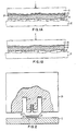
- an IC package comprises a semiconductor chip 10 that is bonded to a substrate 12 by bonding means 14, which may be solder ball connections, by way of example.
- a controlled load force F is applied, as designated by the arrow, by means of a spring 16, for example, to the chip 10 to maximize the surface contact of the chip with a pivotable piston heat transfer element 18 of a high thermal conductivity material such as copper.
- Heat generated in the chip is conducted across the chip interface into the piston element and from the element to the surrounding structure essentially by gaseous conduction across the gap spaces 26.
- the surrounding hat structure 20 provides a cover and additional heat diffusing means for the IC package.
- a low temperature noneutectic bismuth alloy 22 is bonded to the heat transfer element.
- the alloy used is commercially available Ostalloy, a product of Arconium Corp. of America.
- the alloy is composed of 51.45% bismuth, 31.35% lead, 15.20% tin and 2.0% indium, and is characterized by a solidus temperature T s of about 88°C, and a liquidus temperature T L of about 112°C.
- An alternative low melting temperature alloy that may be used has a composition of 48.35% bismuth, 28.15% lead, 14.50% tin and 9.0% antimony, and has a solidus temperature of about 87°C and liquidus temperature of about 128°C. Still other compositions are also practical depending on desired thermal operating conditions of the IC device.
- the bismuth alloy 22 is deposited on the heat sink surface to a thickness of approximately 50.8 um (2 mils), and as illustrated in FIG. 1A, initially only makes actual contact with the surface of the chip 10 at spaced points between voids 24. With this initial condition of the alloy randomly contacting the cold chip surface over a small aggregate heat transfer area, the interface thermal resistance is relatively high, and heat transfer is relatively low.
- the temperature of the device is raised to the melting range of the alloy.
- T c a temperature greater than the solidus temperature T s
- the bismuth alloy melts and conforms under viscous flow conditions by the action of the applied force F, to fill the void spaces 24, as depicted in FIG. 1B.
- the resulting increased contact area and thus the thermal enhanced path between the chip and the heat transfer element through the alloy now filling the voids causes a sharp decrease in thermal resistance at the interface and thus allows effective dissipation of the excessive heat.
- the above local conforming action of the thin alloy layer is confined to the interface region by the controlling action of surface tension forces.
- chip interface thermal resistances of 0.1 to 0.2°C per watt are obtained with contact loads of approximately 0.98 N (100 grams).
- the resistance levels obtained by means of this invention are approximately five to seven times lower than that realized with thermal grease.
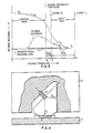
- the process according to this invention is illustrated in FIG. 3.
- the relatively high resistance R H at the time of assembly, is reduced to a low level R L by a reflow operation.
- the resistance Upon reducing the temperature below the maximum operating condition, the resistance remains at such low level R L in the operating temperature range.
- the rise in resistance causes a temperature rise into the pasty range where the resistance and temperature both decrease rapidly back to their initial states.
- the maximum solidus temperature OT MS would be in the order of 1-3°C, while the solidus-liquidus AT SL may be in the range of 15-25°C.
- the system is always in a solid state under normal operating conditions. Any excursions into the solidus-liquidus range for thermal resistance-temperature recovery constitutes a very small time period relative to the product life. Since the system is virtually always in the solid state, contact loads at the interface are low and adverse metallurgical phenomena are essentially eliminated. Also, once the initial low resistance value R L is obtained, any disturbances at the chip surface will cause momentary increases in resistance. These small resistance changes are removed in very short time periods.
- R L initial low resistance value
- R L initial low resistance value
- any disturbances at the chip surface will cause momentary increases in resistance. These small resistance changes are removed in very short time periods.
- the disclosed technique ensures long-term maintenance of low thermal resistance at the chip interface, which is very significant as chip sizes decrease and power dissipation requirements rise.
- this invention can also be applied to other interfaces in a heat sink structure to obtain low thermal resistance.
- a controlled load force F is applied diagonally, as designated by the arrow, by means of a spring 16, for example, to a pivotable piston heat transfer element 18.
- the bismuth alloy 22 is deposited on each surface of the piston to a thickness of approximately 50.8 ⁇ m (2 mils), and as illustrated in FIG. 1A, initially only makes actual contact with the surface of the chip 10 at spaced points between the voids 24. Similarly, the contact of the alloy 22 with the hat 20 surface also involves point contacts and void spaces. With this initial condition of the alloy randomly contacting the cold chip and hat surfaces over a small aggregate heat transfer area, the thermal resistance at the interfaces is relatively high, and heat transfer is relatively low.
- the temperature of the device is raised to the melting range of the alloy.
- T c a temperature greater than the solidus temperature T s
- the bismuth alloy melts and under the action of the applied force component F v , fills the void spaces as described previously.
- the alloy melts at the hat interface, and under the action of the applied force component F H , fills the void spaces in this region.
- the resulting increased contact area at both interfaces causes a sharp decrease in thermal resistances and thus allows effective dissipation of the excessive heat.
- FIG. 3 The process according to this invention is illustrated in FIG. 3 for the case of the chip contact surface condition.
- the process for the hat interface condition is the same as that for the chip contact.
- the relatively high resistances R H at the time of assembly, are reduced to low levels R L by a reflow operation.
- the resistances Upon reducing the temperature below the maximum operating condition, the resistances remain at such low levels R L in the operating temperature range. If disturbance of the interfaces occurs, the self-healing action of the alloy causes a rapid recovery of the low thermal resistances and temperatures in a manner discussed previously in connection with FIG. 3.
- the chip interface thermal resistances of 0.1 to 0.2°C per watt are obtained with contact loads of approximately 0.98 N (100 grams).
- the corresponding preferred hat interface thermal resistances are in the range of 0.01 to 0.02°C per watt.
- FIGS. 2 and 4 represent just two of a number of possible configurations for achieving and maintaining highly effective heat dissipation. With the structure of this invention, applications that require from 9-20 watts/chip heat dissipation are feasible.
Landscapes
- Cooling Or The Like Of Semiconductors Or Solid State Devices (AREA)
Applications Claiming Priority (1)
| Application Number | Priority Date | Filing Date | Title |
|---|---|---|---|
| PCT/US1981/001754 WO1983002363A1 (en) | 1981-12-29 | 1981-12-29 | Cooling means for integrated circuit chip device |
Publications (3)
| Publication Number | Publication Date |
|---|---|
| EP0097157A1 EP0097157A1 (en) | 1984-01-04 |
| EP0097157A4 EP0097157A4 (en) | 1985-03-08 |
| EP0097157B1 true EP0097157B1 (en) | 1987-09-30 |
Family
ID=22161583
Family Applications (1)
| Application Number | Title | Priority Date | Filing Date |
|---|---|---|---|
| EP82900586A Expired EP0097157B1 (en) | 1981-12-29 | 1981-12-29 | Cooling means for integrated circuit chip device |
Country Status (4)
| Country | Link |
|---|---|
| EP (1) | EP0097157B1 (enExample) |
| JP (1) | JPS58501648A (enExample) |
| DE (1) | DE3176475D1 (enExample) |
| WO (1) | WO1983002363A1 (enExample) |
Families Citing this family (6)
| Publication number | Priority date | Publication date | Assignee | Title |
|---|---|---|---|---|
| US4462462A (en) * | 1981-11-17 | 1984-07-31 | International Business Machines Corporation | Thermal conduction piston for semiconductor packages |
| USRE35721E (en) * | 1983-12-14 | 1998-02-03 | Hitachi, Ltd. | Cooling device of semiconductor chips |
| JPS60126853A (ja) * | 1983-12-14 | 1985-07-06 | Hitachi Ltd | 半導体デバイス冷却装置 |
| JPS6115353A (ja) * | 1984-06-29 | 1986-01-23 | インタ−ナショナル ビジネス マシ−ンズ コ−ポレ−ション | チツプ冷却装置 |
| DE19802117C1 (de) * | 1998-01-21 | 1999-06-02 | Fne Gmbh | Thermisch steuerbare Anordnung |
| KR102228516B1 (ko) * | 2019-08-05 | 2021-03-16 | 엘지전자 주식회사 | 다수의 사용자가 포함된 사용자 그룹을 운송하는 자율 주행 차량 및 이의 제어 방법과, 상기 자율 주행 차량을 제어하는 제어 서버 |
Family Cites Families (9)
| Publication number | Priority date | Publication date | Assignee | Title |
|---|---|---|---|---|
| US3271638A (en) * | 1963-11-04 | 1966-09-06 | Emil M Murad | Encased semiconductor with heat conductive and protective insulative encapsulation |
| US3536460A (en) * | 1966-12-28 | 1970-10-27 | Great Lakes Carbon Corp | Connections between electrical conductors and carbon bodies and method of making same |
| US3449818A (en) * | 1967-05-16 | 1969-06-17 | North American Rockwell | Superconductor joint |
| US3996447A (en) * | 1974-11-29 | 1976-12-07 | Texas Instruments Incorporated | PTC resistance heater |
| US3993123A (en) * | 1975-10-28 | 1976-11-23 | International Business Machines Corporation | Gas encapsulated cooling module |
| US4193445A (en) * | 1978-06-29 | 1980-03-18 | International Business Machines Corporation | Conduction cooled module |
| US4203129A (en) * | 1978-07-11 | 1980-05-13 | International Business Machines Corporation | Bubble generating tunnels for cooling semiconductor devices |
| US4323914A (en) * | 1979-02-01 | 1982-04-06 | International Business Machines Corporation | Heat transfer structure for integrated circuit package |
| US4254431A (en) * | 1979-06-20 | 1981-03-03 | International Business Machines Corporation | Restorable backbond for LSI chips using liquid metal coated dendrites |
-
1981
- 1981-12-29 JP JP82500649A patent/JPS58501648A/ja active Granted
- 1981-12-29 DE DE8282900586T patent/DE3176475D1/de not_active Expired
- 1981-12-29 EP EP82900586A patent/EP0097157B1/en not_active Expired
- 1981-12-29 WO PCT/US1981/001754 patent/WO1983002363A1/en not_active Ceased
Non-Patent Citations (1)
| Title |
|---|
| RÖMPPS Chemie-Lexikon, FRANCKH'sche Verlagshandlung, Stuttgart, page 2405 * |
Also Published As
| Publication number | Publication date |
|---|---|
| EP0097157A4 (en) | 1985-03-08 |
| DE3176475D1 (en) | 1987-11-05 |
| EP0097157A1 (en) | 1984-01-04 |
| JPS6222531B2 (enExample) | 1987-05-19 |
| WO1983002363A1 (en) | 1983-07-07 |
| JPS58501648A (ja) | 1983-09-29 |
Similar Documents
| Publication | Publication Date | Title |
|---|---|---|
| US4607277A (en) | Semiconductor assembly employing noneutectic alloy for heat dissipation | |
| US6281573B1 (en) | Thermal enhancement approach using solder compositions in the liquid state | |
| US7078109B2 (en) | Heat spreading thermal interface structure | |
| US7960019B2 (en) | Phase change material containing fusible particles as thermally conductive filler | |
| US7369411B2 (en) | Thermal interface assembly and method for forming a thermal interface between a microelectronic component package and heat sink | |
| US5012858A (en) | Method of cooling a semiconductor device with a cooling unit, using metal sherbet between the device and the cooling unit | |
| US7429502B2 (en) | Integrated circuit device incorporating metallurgical bond to enhance thermal conduction to a heat sink | |
| US7311967B2 (en) | Thermal interface material and electronic assembly having such a thermal interface material | |
| EP0061592B1 (en) | Electronic package | |
| EP0385605A2 (en) | Integrated circuit/heat sink interface device | |
| EP0473929B1 (en) | Method of forming a thin film electronic device | |
| KR100705868B1 (ko) | 반도체 장치 및 그 제조 방법 | |
| WO2002011504A2 (en) | Thermal interface material on a mesh carrier | |
| EP0097157B1 (en) | Cooling means for integrated circuit chip device | |
| TWI484604B (zh) | 金屬熱界面材料以及含該材料的構裝半導體 | |
| US20030230403A1 (en) | Conductive thermal interface and compound | |
| JP6144440B1 (ja) | 半導体封止用プリフォーム | |
| US3480842A (en) | Semiconductor structure disc having pn junction with improved heat and electrical conductivity at outer layer | |
| EP4163963B9 (en) | Heat conduction member, single board, computing device and manufacturing method | |
| JP2011155227A (ja) | 半導体装置及びその製造方法 | |
| JPH0382145A (ja) | 半導体装置およびその製造方法 | |
| EP1601012A2 (en) | Microelectronic assembly having variable thickness solder joint | |
| JPS61171153A (ja) | 半導体装置 | |
| Jensen et al. | Reinforced solder preforms for high-reliability and low voiding | |
| JPS60239049A (ja) | 熱伝導冷却モジユ−ル装置 |
Legal Events
| Date | Code | Title | Description |
|---|---|---|---|
| PUAI | Public reference made under article 153(3) epc to a published international application that has entered the european phase |
Free format text: ORIGINAL CODE: 0009012 |
|
| 17P | Request for examination filed |
Effective date: 19830809 |
|
| AK | Designated contracting states |
Kind code of ref document: A1 Designated state(s): DE FR GB |
|
| 17Q | First examination report despatched |
Effective date: 19860616 |
|
| R17C | First examination report despatched (corrected) |
Effective date: 19860618 |
|
| GRAA | (expected) grant |
Free format text: ORIGINAL CODE: 0009210 |
|
| AK | Designated contracting states |
Kind code of ref document: B1 Designated state(s): DE FR GB |
|
| REF | Corresponds to: |
Ref document number: 3176475 Country of ref document: DE Date of ref document: 19871105 |
|
| ET | Fr: translation filed | ||
| PLBE | No opposition filed within time limit |
Free format text: ORIGINAL CODE: 0009261 |
|
| STAA | Information on the status of an ep patent application or granted ep patent |
Free format text: STATUS: NO OPPOSITION FILED WITHIN TIME LIMIT |
|
| 26N | No opposition filed | ||
| PGFP | Annual fee paid to national office [announced via postgrant information from national office to epo] |
Ref country code: DE Payment date: 19911221 Year of fee payment: 11 |
|
| PGFP | Annual fee paid to national office [announced via postgrant information from national office to epo] |
Ref country code: FR Payment date: 19921124 Year of fee payment: 12 |
|
| PGFP | Annual fee paid to national office [announced via postgrant information from national office to epo] |
Ref country code: GB Payment date: 19921126 Year of fee payment: 12 |
|
| PG25 | Lapsed in a contracting state [announced via postgrant information from national office to epo] |
Ref country code: DE Effective date: 19930901 |
|
| PG25 | Lapsed in a contracting state [announced via postgrant information from national office to epo] |
Ref country code: GB Effective date: 19931229 |
|
| GBPC | Gb: european patent ceased through non-payment of renewal fee |
Effective date: 19931229 |
|
| PG25 | Lapsed in a contracting state [announced via postgrant information from national office to epo] |
Ref country code: FR Effective date: 19940831 |
|
| REG | Reference to a national code |
Ref country code: FR Ref legal event code: ST |