EP0094767A1 - Devices for generating three-phase PWM waveforms for control of induction motors - Google Patents
Devices for generating three-phase PWM waveforms for control of induction motors Download PDFInfo
- Publication number
- EP0094767A1 EP0094767A1 EP83302537A EP83302537A EP0094767A1 EP 0094767 A1 EP0094767 A1 EP 0094767A1 EP 83302537 A EP83302537 A EP 83302537A EP 83302537 A EP83302537 A EP 83302537A EP 0094767 A1 EP0094767 A1 EP 0094767A1
- Authority
- EP
- European Patent Office
- Prior art keywords
- motor
- microprocessor
- control
- waveform
- analog
- Prior art date
- Legal status (The legal status is an assumption and is not a legal conclusion. Google has not performed a legal analysis and makes no representation as to the accuracy of the status listed.)
- Withdrawn
Links
- 230000006698 induction Effects 0.000 title claims abstract description 16
- 238000012545 processing Methods 0.000 claims description 3
- 230000008859 change Effects 0.000 abstract description 2
- 238000000034 method Methods 0.000 description 11
- 238000010586 diagram Methods 0.000 description 5
- 230000006870 function Effects 0.000 description 5
- 238000012360 testing method Methods 0.000 description 5
- 239000000872 buffer Substances 0.000 description 4
- 238000006243 chemical reaction Methods 0.000 description 4
- 230000004044 response Effects 0.000 description 4
- 238000013461 design Methods 0.000 description 3
- 230000008569 process Effects 0.000 description 3
- 230000001143 conditioned effect Effects 0.000 description 2
- 230000002441 reversible effect Effects 0.000 description 2
- 230000004913 activation Effects 0.000 description 1
- 230000004075 alteration Effects 0.000 description 1
- 230000009286 beneficial effect Effects 0.000 description 1
- 230000008901 benefit Effects 0.000 description 1
- 238000004364 calculation method Methods 0.000 description 1
- 230000000295 complement effect Effects 0.000 description 1
- 230000003750 conditioning effect Effects 0.000 description 1
- 230000003247 decreasing effect Effects 0.000 description 1
- 230000001419 dependent effect Effects 0.000 description 1
- 230000004048 modification Effects 0.000 description 1
- 230000002093 peripheral effect Effects 0.000 description 1
- 238000004886 process control Methods 0.000 description 1
- 230000009467 reduction Effects 0.000 description 1
- 230000002194 synthesizing effect Effects 0.000 description 1
- 230000001052 transient effect Effects 0.000 description 1
Images


Classifications
-
- H—ELECTRICITY
- H02—GENERATION; CONVERSION OR DISTRIBUTION OF ELECTRIC POWER
- H02M—APPARATUS FOR CONVERSION BETWEEN AC AND AC, BETWEEN AC AND DC, OR BETWEEN DC AND DC, AND FOR USE WITH MAINS OR SIMILAR POWER SUPPLY SYSTEMS; CONVERSION OF DC OR AC INPUT POWER INTO SURGE OUTPUT POWER; CONTROL OR REGULATION THEREOF
- H02M7/00—Conversion of AC power input into DC power output; Conversion of DC power input into AC power output
- H02M7/42—Conversion of DC power input into AC power output without possibility of reversal
- H02M7/44—Conversion of DC power input into AC power output without possibility of reversal by static converters
- H02M7/48—Conversion of DC power input into AC power output without possibility of reversal by static converters using discharge tubes with control electrode or semiconductor devices with control electrode
- H02M7/53—Conversion of DC power input into AC power output without possibility of reversal by static converters using discharge tubes with control electrode or semiconductor devices with control electrode using devices of a triode or transistor type requiring continuous application of a control signal
- H02M7/537—Conversion of DC power input into AC power output without possibility of reversal by static converters using discharge tubes with control electrode or semiconductor devices with control electrode using devices of a triode or transistor type requiring continuous application of a control signal using semiconductor devices only, e.g. single switched pulse inverters
- H02M7/5387—Conversion of DC power input into AC power output without possibility of reversal by static converters using discharge tubes with control electrode or semiconductor devices with control electrode using devices of a triode or transistor type requiring continuous application of a control signal using semiconductor devices only, e.g. single switched pulse inverters in a bridge configuration
- H02M7/53871—Conversion of DC power input into AC power output without possibility of reversal by static converters using discharge tubes with control electrode or semiconductor devices with control electrode using devices of a triode or transistor type requiring continuous application of a control signal using semiconductor devices only, e.g. single switched pulse inverters in a bridge configuration with automatic control of output voltage or current
- H02M7/53873—Conversion of DC power input into AC power output without possibility of reversal by static converters using discharge tubes with control electrode or semiconductor devices with control electrode using devices of a triode or transistor type requiring continuous application of a control signal using semiconductor devices only, e.g. single switched pulse inverters in a bridge configuration with automatic control of output voltage or current with digital control
-
- H—ELECTRICITY
- H02—GENERATION; CONVERSION OR DISTRIBUTION OF ELECTRIC POWER
- H02M—APPARATUS FOR CONVERSION BETWEEN AC AND AC, BETWEEN AC AND DC, OR BETWEEN DC AND DC, AND FOR USE WITH MAINS OR SIMILAR POWER SUPPLY SYSTEMS; CONVERSION OF DC OR AC INPUT POWER INTO SURGE OUTPUT POWER; CONTROL OR REGULATION THEREOF
- H02M7/00—Conversion of AC power input into DC power output; Conversion of DC power input into AC power output
- H02M7/42—Conversion of DC power input into AC power output without possibility of reversal
- H02M7/44—Conversion of DC power input into AC power output without possibility of reversal by static converters
- H02M7/48—Conversion of DC power input into AC power output without possibility of reversal by static converters using discharge tubes with control electrode or semiconductor devices with control electrode
- H02M7/505—Conversion of DC power input into AC power output without possibility of reversal by static converters using discharge tubes with control electrode or semiconductor devices with control electrode using devices of a thyratron or thyristor type requiring extinguishing means
- H02M7/515—Conversion of DC power input into AC power output without possibility of reversal by static converters using discharge tubes with control electrode or semiconductor devices with control electrode using devices of a thyratron or thyristor type requiring extinguishing means using semiconductor devices only
- H02M7/525—Conversion of DC power input into AC power output without possibility of reversal by static converters using discharge tubes with control electrode or semiconductor devices with control electrode using devices of a thyratron or thyristor type requiring extinguishing means using semiconductor devices only with automatic control of output waveform or frequency
- H02M7/527—Conversion of DC power input into AC power output without possibility of reversal by static converters using discharge tubes with control electrode or semiconductor devices with control electrode using devices of a thyratron or thyristor type requiring extinguishing means using semiconductor devices only with automatic control of output waveform or frequency by pulse width modulation
- H02M7/529—Conversion of DC power input into AC power output without possibility of reversal by static converters using discharge tubes with control electrode or semiconductor devices with control electrode using devices of a thyratron or thyristor type requiring extinguishing means using semiconductor devices only with automatic control of output waveform or frequency by pulse width modulation using digital control
Definitions
- This invention relates to devices or apparatus for generating digital three-phase pulse width modulated (PWM) waveforms which can be used for constant torque variable speed control of induction motors, for example for closed loop position control.
- PWM pulse width modulated
- a device for generating three-phase pulse width modulated waveforms for constant torque variable speed control of an induction motor the device being characterised by:
- real time software is utilized in the microprocessor to control the pulse width modulated waveform (PWM) shape and also to control logic involving interrupt and control signals.
- PWM pulse width modulated waveform
- the use of real time software increases the flexibility of the system to adapt to different conditions and applications.
- Digital techniques are used in the preferred device to generate the PWM waveforms.
- the close interrelationship between the hardware (microprocessor and related peripherals) and the real time software allow efficient generation and control of the PWM waveforms for both open loop and closed loop systems.
- the preferred device is such as to allow the easy alteration of the control techniques and PWM generation for closed or open loop control with no hardware redesign involved.
- Necessary changes required for different applications can be implemented in the real time software, the microprocessor being programmable so as to adapt to different control requirements and conditions. No factory calibration is required after the real-time software is configured for the intended application.
- the preferred device alleviates or overcomes the drawbacks of an analog modulation device and generates waveforms for any assigned output level.
- the drawings show a device embodying the invention for generating three-phase pulse width modulated (PWM) waveforms allowing variable speed control of an induction motor.
- PWM pulse width modulated
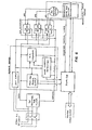
- the waveform generation is implemented by hardware and real time software, which is completely contained on a circuit card designated as a position control module (PCM) 10 in Figure 1.
- PCM 10 is an integral part of another system designated a three phase drive controller and shown in Figure 6.
- the three phase drive controller controls the motion of a motor to set the position of dampers, air registers, butterfly valves, or other process control elements which require a motor or servo positioner to control their position from a remote location.
- the PCM 10 provides intelligence for the three phase drive controller.
- the PCM 10 is a self-contained microcomputer which accepts control system inputs and, based on those inputs, develops logic level PWM waveforms which are applied to three power switching modules which are external to the PCM.
- the PCM uses a MC6802 microprocessor 12 with up to 4K bytes of program storage.
- the processor 12 is an interrupt driven machine with priority given to updating the real time three phase (30) PWM waveform outputs to the induction motor.
- the remaining processor time is used to check control system inputs, perform calculations, and display controller status.
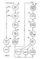
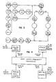
- FIG. 1 A functional diagram of the hardware of the PCM 10 is shown in Figure 1.
- FIG. 6 A schematic of the PCM is shown in Figure 6, in the three-phase drive controller.
- a microprocessor based system for three phase motor control is more versatile than a dedicated analog or digital logic design.
- the ease of software modification allows the functional performance of the controller to be easily changed to a new application.
- the microprocessor 12 used in the PCM as a central control unit is a Motorola 6802.
- the 6802 processor 12 includes 128 bytes of RAM and an onboard system clock.
- the control software requires approximately 3K bytes of memory.
- the software is stored in a 4K ultra violet erasable read only memory (ROM) 14 such as a 25L32 or 27L32 device. These devices have access times of 450 nsec, which is sufficient for this application.
- ROM addresses are located at the top of the memory from $F000 to $FFFF.
- the control program uses only the 128 bytes of RAM located on the 6802 microprocessor 12.
- the RAM is used for buffers and variable storage.
- the RAM address locations are from $0000 to $007F.
- the design includes two Motorola 6840 programmable timer modules (PTM) 16 and 18. Three individual timers are located on one LSI device. The timers are used to generate output waveform pulse patterns at 20, measure time variant digital inputs, generate interrupts, and provide a machine fault time (MFT) function.
- PTM programmable timer modules
- MFT machine fault time
- the timers (16, 18) are operated in a single shot mode. This mode allows a 16 bit binary number to be loaded into a timer latch. Count down is initiated through software or external logic control. A complete countdown to 0 of the 16 bit binary number generates an interrupt, or changes the state of the output associated with that timer. The rate at which count down occurs is determined by the system clock or an external clock source.
- Fourtimers are dedicated to the generation of the three pulse width modulated waveforms 20.
- One timer is a master timer (in 16) which generates processor interrupts at a rate proportional to the output frequency of the controller.
- the interrupt routine updates the other three timers, each dedicated to aphase output, with the new PWM waveform values.
- the processor timernot associated with the interrupt routine is used to complete the main task of the control software to be described later.
- the use of the timers minimizes the processor overhead associated with the generation of the PWM waveforms.
- the digital system inputs 22 are all TTL logic level.
- the incoming digital inputs are all filtered at 24 to eliminate noise generated by high power inverter circuitry.
- transient protection is provided to suppress electrical surges.
- the inputs are buffered and interfaced to the processor by an octal buffer 26.
- Digital signals which are outputted by the processor 12 for control of the PWM waveform 20, mode status at latch 32, and analog multiplexing,interface to their associated circuitry by octal latches.
- the octal latches are a low cost method of digital interface for a given dedicated application.
- the latch 32 dedicated to controller mode display 28 is configured to allow data bus information from line 30 to be displayed under program control. This feature is beneficial for both testing and analog calibrations at 28.
- Latches, buffers, programmable timers, memory, and the analog to digital converter are all memory mapped by a 3 to 8 digital decoder 36.
- the decoder segments the memory into 8 addressable zones. All necessary logic has been included to ensure the proper timing of data, address, and chip select lines.
- a machine fault timer (MFT) in 16 has been provided on the PCM 10 to reset the processor 12 in the event a noise pulse or bad address disturbs the normal software execution.
- the MFT is updated by the processor during a regular known program sequence. The absence of this update implies a software failure.
- the MFT times out and rests the processor, reinitializing the system as will be described later.
- the PCM 10 Four analog signals at line 38 are recognized by the PCM 10. Two represent the gain and deadband control parameters which are generated internally by potentiometers. These parameters are associated with closed loop position control. They can easily be redefined in software for other applications. The remaining two are the setpoint and the feedback analog inputs which originate from a control system (Fig. 6) . Each analog signal has the voltage range of 0.75 to 5.25V dc. The feedback and setpoint signals, in addition, can be 4-20 mA signals which are converted to voltages by the PCM. The advantage of a current input signal is reduced noise and no attenuation due to long signal wires. The feedback signal is buffered and outputed to the control system for other control applications.
- the four analog voltages are selected individually for A/D (analog to digital) conversion by an analog multiplexer 40 under processor control.
- the selected analog voltage is applied to a level shifter and filter 42 for proper signal conditioning before the 8 bit A/D conversion 44.
- the A/D converter 44 has an adjustable zero and span allowing maximum resolution for the given input voltage range. The span and zero are adjusted for allowing the 0.75 and 5.25V dc input range (corresponds to -5% to 105% of variable) to convert from 0 to 255 counts of digital data.
- the A/D interfaces to the processors by internally contained three state buffers which are controlled by the processor 12.
- Accurate conversions are possible by proper printed circuit layout and component selection. Reduction of digital noise generated by the microprocessor is reduced by separating the analog and digital ground returns, placement of components, and physically segregating all analog components from digital components. The component tolerances and temperature coefficients are selected such that an accuracy of more than 0.3% is maintained across the temperature range of 4° C to 60° C (40° to 140° F).
- the PWM waveform 20 which is outputed by the programmable timers is conditioned at 46 before being applied to the phase driver inputs 48.
- the activation of the positive and negative phase outputs are non-overlapping to ensure safe operation of the 3 phase inverter.
- a 24 microsecond dead time is created by a shift register and various logic elements.
- a processor controlled latch 34 generates waveform inversion signals which are combined with the timer outputs 20 to reduce the memory table associated with the waveforms by 50%. This same latch 34 has the capability to interrupt the waveform outputs instantly under program control.
- the conditioned waveform outputs are buffered by a D arlington transistor package before leaving the PCM at 48.
- the most active interrupt is generated by the master timer.
- the master timer (also in 16) generates maskable interrupts proportional to the desired output frequency.
- the interrupt is electrically generated by the 6840 PTM 16.
- the second interrupt (overcurrent condition) is generated by circuitry external to the PCM. This interrupt is also processed by the maskable interrupt of the processor.
- the two interrupts are distinguished by polling the 6840 timer 16.
- the functions of the microprocessor 12, according to the processor software, are as follows.
- the microprocessor must read inputs, decide what mode is being input, and process that mode. Then the processor must determine the proper frequency, and output this frequency via the programmable timer 18.
- Figures 2 and 3 show a state diagram overview of these functions.
- Fig. 4 shows the analog and digital interface to the processor.
- the processor software is written entirely in machine code to maximize processor time available for response to control system parameters.
- the microprocessor 12 After receiving a RESET input at 11, the microprocessor 12, as shown in Fig. 2, goes into a normal software reset - RAM test (52), ROM checksum test (54), etting of the stack pointer (56), initializing both programmable times (58,60), setting up Machine Fault Timer, setting up pulse storage timer, and setting up the first IRQ timer value.
- the main task of the processor 12 handles analog conversions, checks limit conditions, checks feedback, ramps frequency, and checks the mode of operation.
- the processor 12 converts the analog signals.
- the analog signals are converted to hexadecimal and stored in RAM for use later. Each analog signal thus converted is determined by the input of the multiplexer 40.
- limit checking occurs (70). If either limit is set (u p or down), the DESFRQ (Desired Frequency) is set to zero. Then as long as a limit is set, the DESFRQ equals zero only in the direction of the limit. This causes the motor to be able to run in the opposite direction of the limit condition.
- the limit inputs can be externally configured to provide system control of the motor.
- the ramping of frequency (74) only occurs after so many passes of the wave pulse output.
- the processor decides if the actual direction (ACTDIR) is equal to the desired direction (DESDIR). If the directions are not equal, the ACTFRQ must be ramped down to 0 Hz (motor stopped) before the directions can be set equal, the processor decides whether to ramp the frequency or not, and if so, in which direction. The following tests are made and the results are as follows:
- the next task is mode selection (76).
- This portion of the real time software can be configured to allow control of a particular application. This section of the software will contain all applicable control algorithms for a given application. The ACTFRQ and DESFRQ values are determined in this portion of the software.
- the IRQ interrupt is used for an over-current condition and wave-pulse output, as shown in Fig. 3.
- Over- current condition is noted by hardware, which gives the processor an IRQ interrupt.
- the response of the processor to an over- current interrupt is dependent on the application. If the over- current condition is determined undesirable, the motor is turned off and a manual RESET must occur to INITIALIZE the controller again.
- the desired outputs are three sine-waves 90, 92, 94 in Fig. 5, which are used to drive the three phases of a three-phase induction motor.
- the three sine-waves either lead or lag each other by 120° per phase.
- a reverse in the phasing of the sine-waves results in a reverse in the direction of the motor.
- the establishment of the square pulse patterns 96, 98, 100, leading to the superimposed sine wave, is known as pulse width modulation.
- Twenty-four, thirty-six, seventy-two or one-hundred and fourty-four equal pulses (frequency determining the number) with varying "on-times" are used to generate the sine wave of the desired frequency.
- the number of pulses per cycle can be altered for any given frequency under software control.
- Thirty-six pulses are used in Fig. 5.
- the "on-time" for each pulse is calculated from the following formula:
- Fig. 5 shows the pulse pattern sine wave relation- ship. The negative half of the sine-wave is derived from the complement of this signal.
- the method for each of the three phase wave- forms is the same.
- the ROM 14 contains 20 different tables. each table corresponds to a different output waveform frequency from 3 to 60 Hz in 3 Hz increments).
- the entries each table are the programmable timer values necessary create 90 degrees of a 360degree PWM sine wave. The entire wave is created by repeating the entries in the table in proper sequence and propercontrol of the waveform inversion control lines outputed by latch 34. Only one table is necessary generate all three phase outputs. The individual phases require the same timer values for a given frequency. It is necessary to displace the three waveforms by 120° with respect to each other.
- each frequen- table do not necessarily have to be sine weighted.
- the values can be changed to provide non-sinusoidal waveforms achieve greater average voltage output resulting in a different motor torque relationship.
- PNTA, PNTB and PNTC are the pointers for the three phases A, B and C; FRQPT is frequency point; and CNTA, CNTR, CNTC are the counts for the three phases.
- the output for each phase is similar regardles of the number of pulses .
- a 36 pulse output will be shown in more detail.
- the pointers move up and down the table depei on the value of the counter that it is associated with. See Tables II and III for an example of this.
- a gate is also set reset, depending on the count of the counter for each phase. When the counter reaches its limit, it is set to zero and the process starts over again.
- Pointers (PNT) B and c start at the same location but more in opposite directions because of CNT values.
- the time required to process an IRQ interrupt directly affects the overall system response of the PCM 10.
- the IRQ routine is given top priority to allow the real time PWM waveform outputs 48 to continue without interruption
- the IRQ execution time is reduced by the use of efficient machine instructions at the expense of increased memory locations necessary to store the IRQ routine.
Landscapes
- Engineering & Computer Science (AREA)
- Power Engineering (AREA)
- Control Of Ac Motors In General (AREA)
- Control Of Stepping Motors (AREA)
- Stopping Of Electric Motors (AREA)
Applications Claiming Priority (2)
| Application Number | Priority Date | Filing Date | Title |
|---|---|---|---|
| US37579682A | 1982-05-07 | 1982-05-07 | |
| US375796 | 1982-05-07 |
Publications (1)
| Publication Number | Publication Date |
|---|---|
| EP0094767A1 true EP0094767A1 (en) | 1983-11-23 |
Family
ID=23482385
Family Applications (1)
| Application Number | Title | Priority Date | Filing Date |
|---|---|---|---|
| EP83302537A Withdrawn EP0094767A1 (en) | 1982-05-07 | 1983-05-05 | Devices for generating three-phase PWM waveforms for control of induction motors |
Country Status (9)
| Country | Link |
|---|---|
| EP (1) | EP0094767A1 (enExample) |
| JP (2) | JPS5921295A (enExample) |
| KR (1) | KR900000769B1 (enExample) |
| AU (1) | AU560498B2 (enExample) |
| BR (1) | BR8302459A (enExample) |
| CA (1) | CA1202364A (enExample) |
| ES (1) | ES8404580A1 (enExample) |
| IN (1) | IN159296B (enExample) |
| MX (1) | MX153611A (enExample) |
Cited By (3)
| Publication number | Priority date | Publication date | Assignee | Title |
|---|---|---|---|---|
| GB2149242A (en) * | 1983-09-30 | 1985-06-05 | Matsushita Electric Industrial Co Ltd | Inverter controlling apparatus for induction motor drive |
| EP0301483A3 (en) * | 1987-07-27 | 1989-11-15 | Kabushiki Kaisha Toshiba | Control apparatus for a power converter |
| CN102185555A (zh) * | 2010-12-28 | 2011-09-14 | 上海智大电子有限公司 | 一种数字化交流调压调速装置 |
Families Citing this family (3)
| Publication number | Priority date | Publication date | Assignee | Title |
|---|---|---|---|---|
| JPS61248713A (ja) * | 1985-04-26 | 1986-11-06 | Nissei Plastics Ind Co | 回転式射出成形機 |
| JPS61251484A (ja) * | 1985-04-26 | 1986-11-08 | Mitsubishi Electric Corp | インバ−タ装置のpwm制御回路 |
| US6644310B1 (en) * | 2000-09-29 | 2003-11-11 | Mallinckrodt Inc. | Apparatus and method for providing a breathing gas employing a bi-level flow generator with an AC synchronous motor |
Citations (6)
| Publication number | Priority date | Publication date | Assignee | Title |
|---|---|---|---|---|
| US4099109A (en) * | 1976-10-01 | 1978-07-04 | Westinghouse Electric Corp. | Digital apparatus for synthesizing pulse width modulated waveforms and digital pulse width modulated control system |
| US4105939A (en) * | 1976-08-10 | 1978-08-08 | Westinghouse Electric Corp. | Direct digital technique for generating an AC waveform |
| GB2025175A (en) * | 1978-07-06 | 1980-01-16 | Siemens Ag | Digital generation of waveforms controlling inverters |
| JPS5610091A (en) * | 1979-07-02 | 1981-02-02 | Hitachi Ltd | Controlling device for electric motor |
| GB2079979A (en) * | 1980-06-20 | 1982-01-27 | Kollmorgen Tech Corp | Electromechanical Energy Conversion System |
| EP0063176A2 (de) * | 1981-04-16 | 1982-10-27 | Siemens Aktiengesellschaft | Steuersatz für einen Wechselrichter |
Family Cites Families (2)
| Publication number | Priority date | Publication date | Assignee | Title |
|---|---|---|---|---|
| JPS55125086A (en) * | 1979-03-20 | 1980-09-26 | Hitachi Ltd | Motor controlling device |
| JPS5771274A (en) * | 1980-10-20 | 1982-05-04 | Toshiba Corp | Controlling device for inverter |
-
1983
- 1983-04-28 ES ES521935A patent/ES8404580A1/es not_active Expired
- 1983-05-03 KR KR1019830001889A patent/KR900000769B1/ko not_active Expired
- 1983-05-04 MX MX197184A patent/MX153611A/es unknown
- 1983-05-04 IN IN547/CAL/83A patent/IN159296B/en unknown
- 1983-05-05 EP EP83302537A patent/EP0094767A1/en not_active Withdrawn
- 1983-05-06 CA CA000427649A patent/CA1202364A/en not_active Expired
- 1983-05-06 JP JP58078398A patent/JPS5921295A/ja active Pending
- 1983-05-06 AU AU14304/83A patent/AU560498B2/en not_active Ceased
- 1983-05-09 BR BR8302459A patent/BR8302459A/pt not_active IP Right Cessation
-
1991
- 1991-01-22 JP JP005747U patent/JPH0560193U/ja active Pending
Patent Citations (6)
| Publication number | Priority date | Publication date | Assignee | Title |
|---|---|---|---|---|
| US4105939A (en) * | 1976-08-10 | 1978-08-08 | Westinghouse Electric Corp. | Direct digital technique for generating an AC waveform |
| US4099109A (en) * | 1976-10-01 | 1978-07-04 | Westinghouse Electric Corp. | Digital apparatus for synthesizing pulse width modulated waveforms and digital pulse width modulated control system |
| GB2025175A (en) * | 1978-07-06 | 1980-01-16 | Siemens Ag | Digital generation of waveforms controlling inverters |
| JPS5610091A (en) * | 1979-07-02 | 1981-02-02 | Hitachi Ltd | Controlling device for electric motor |
| GB2079979A (en) * | 1980-06-20 | 1982-01-27 | Kollmorgen Tech Corp | Electromechanical Energy Conversion System |
| EP0063176A2 (de) * | 1981-04-16 | 1982-10-27 | Siemens Aktiengesellschaft | Steuersatz für einen Wechselrichter |
Non-Patent Citations (2)
| Title |
|---|
| IEEE TRANSACTIONS ON INDUSTRIAL ELECTRONICS AND CONTROL INSTRUMENTATION, vol. IECI-28, no. 3, August 1981, New York G. OLIVIER et al. "Microprocessor controller for a thyristor converter with an improved power factor", pages 188-194 * |
| Patent Abstracts of Japan vol. 5, no. 59, 22 April 1981 & JP-A-56-10091 * |
Cited By (4)
| Publication number | Priority date | Publication date | Assignee | Title |
|---|---|---|---|---|
| GB2149242A (en) * | 1983-09-30 | 1985-06-05 | Matsushita Electric Industrial Co Ltd | Inverter controlling apparatus for induction motor drive |
| EP0301483A3 (en) * | 1987-07-27 | 1989-11-15 | Kabushiki Kaisha Toshiba | Control apparatus for a power converter |
| CN102185555A (zh) * | 2010-12-28 | 2011-09-14 | 上海智大电子有限公司 | 一种数字化交流调压调速装置 |
| CN102185555B (zh) * | 2010-12-28 | 2013-05-08 | 上海智大电子有限公司 | 一种数字化交流调压调速装置 |
Also Published As
| Publication number | Publication date |
|---|---|
| ES521935A0 (es) | 1984-05-01 |
| JPH0560193U (ja) | 1993-08-06 |
| AU1430483A (en) | 1983-11-10 |
| CA1202364A (en) | 1986-03-25 |
| KR900000769B1 (ko) | 1990-02-15 |
| MX153611A (es) | 1986-12-03 |
| BR8302459A (pt) | 1984-01-17 |
| JPS5921295A (ja) | 1984-02-03 |
| ES8404580A1 (es) | 1984-05-01 |
| KR840004630A (ko) | 1984-10-22 |
| IN159296B (enExample) | 1987-05-02 |
| AU560498B2 (en) | 1987-04-09 |
Similar Documents
| Publication | Publication Date | Title |
|---|---|---|
| EP0092937B1 (en) | Three phase variable frequency constant torque controllers for high torque servo positioners | |
| US4599550A (en) | Digital generation of 3-phase PWM waveforms for variable speed control of induction motor | |
| US4419615A (en) | Method of controlling pulse width modulated inverter for use in induction motor drive | |
| EP0401293B1 (en) | Microstepping of an unipolar d.c. motor | |
| EP0772285B1 (en) | Enhanced resolution pulse width modulation control | |
| EP0316006B1 (en) | Pwm controller | |
| CA1095983A (en) | Direct digital technique for generating an ac waveform | |
| EP0140348B1 (en) | Method and apparatus for controlling pwm inverter | |
| EP0094767A1 (en) | Devices for generating three-phase PWM waveforms for control of induction motors | |
| EP0242344B1 (en) | Method and apparatus for controlling a motor | |
| KR880002076A (ko) | 수치제어장치 | |
| US5272430A (en) | System for controlling an inverter through pulse width modulation | |
| JPH11252992A5 (ja) | 直列多重パルス幅変調サイクロコンバータ装置およびその制御方法 | |
| JPS6154890A (ja) | Dcモ−タの制御装置 | |
| SU1577060A1 (ru) | Электропривод переменного тока | |
| Brickwedde et al. | Microprocessor controlled 50KVA PWM inverter motor drive | |
| Bonert | The microprocessor as a tool in the teaching of power electronic circuits and controlled electric drives | |
| SU731550A1 (ru) | Одноканальное устройство дл управлени многофазным вентильным преобразователем | |
| SU1124418A1 (ru) | Частотно-управл емый электропривод | |
| SU849146A1 (ru) | Устройство дл программного управлени шАгОВыМ дВигАТЕлЕМ | |
| SU1094022A1 (ru) | Цифровой регул тор | |
| SU1709485A1 (ru) | Цифровой электропривод посто нного тока | |
| KR0165451B1 (ko) | 위치 제어신호 발생회로 | |
| KR920002587B1 (ko) | 공진형 인버터의 최적출력전류제어시스템 | |
| SU758067A1 (ru) | Устройство для автоматического установа регулируемого объекта в заданное положение 1 |
Legal Events
| Date | Code | Title | Description |
|---|---|---|---|
| PUAI | Public reference made under article 153(3) epc to a published international application that has entered the european phase |
Free format text: ORIGINAL CODE: 0009012 |
|
| AK | Designated contracting states |
Designated state(s): DE FR GB IT |
|
| 17P | Request for examination filed |
Effective date: 19840411 |
|
| STAA | Information on the status of an ep patent application or granted ep patent |
Free format text: STATUS: THE APPLICATION HAS BEEN WITHDRAWN |
|
| 18W | Application withdrawn |
Withdrawal date: 19851028 |
|
| RIN1 | Information on inventor provided before grant (corrected) |
Inventor name: SIEGEL, STUART B. Inventor name: ROBERTSON, JOHN W., JR. |