EP0093531A2 - Verfahren zum rechnergestützten "in-circuit"-Prüfen elektrischer Komponenten und dergleichen mit automatischer Nebensignalunterdrückung - Google Patents
Verfahren zum rechnergestützten "in-circuit"-Prüfen elektrischer Komponenten und dergleichen mit automatischer Nebensignalunterdrückung Download PDFInfo
- Publication number
- EP0093531A2 EP0093531A2 EP83302171A EP83302171A EP0093531A2 EP 0093531 A2 EP0093531 A2 EP 0093531A2 EP 83302171 A EP83302171 A EP 83302171A EP 83302171 A EP83302171 A EP 83302171A EP 0093531 A2 EP0093531 A2 EP 0093531A2
- Authority
- EP
- European Patent Office
- Prior art keywords
- components
- circuit
- signals
- component
- test
- Prior art date
- Legal status (The legal status is an assumption and is not a legal conclusion. Google has not performed a legal analysis and makes no representation as to the accuracy of the status listed.)
- Withdrawn
Links
- 238000012360 testing method Methods 0.000 title claims abstract description 110
- 238000000034 method Methods 0.000 title claims description 43
- 230000001629 suppression Effects 0.000 title description 6
- 230000002401 inhibitory effect Effects 0.000 claims abstract description 19
- 238000012545 processing Methods 0.000 claims abstract description 7
- 230000005540 biological transmission Effects 0.000 claims abstract 4
- 230000008569 process Effects 0.000 claims description 5
- 238000004590 computer program Methods 0.000 claims description 3
- 230000000694 effects Effects 0.000 claims description 3
- 238000013459 approach Methods 0.000 description 4
- 230000008859 change Effects 0.000 description 4
- 230000008054 signal transmission Effects 0.000 description 4
- 238000010586 diagram Methods 0.000 description 3
- 230000006870 function Effects 0.000 description 3
- 230000002452 interceptive effect Effects 0.000 description 3
- 230000000712 assembly Effects 0.000 description 2
- 238000000429 assembly Methods 0.000 description 2
- 230000000875 corresponding effect Effects 0.000 description 2
- 238000002955 isolation Methods 0.000 description 2
- 238000005259 measurement Methods 0.000 description 2
- 230000003466 anti-cipated effect Effects 0.000 description 1
- 230000008901 benefit Effects 0.000 description 1
- 239000003990 capacitor Substances 0.000 description 1
- 230000002596 correlated effect Effects 0.000 description 1
- RUZYUOTYCVRMRZ-UHFFFAOYSA-N doxazosin Chemical compound C1OC2=CC=CC=C2OC1C(=O)N(CC1)CCN1C1=NC(N)=C(C=C(C(OC)=C2)OC)C2=N1 RUZYUOTYCVRMRZ-UHFFFAOYSA-N 0.000 description 1
- 230000005764 inhibitory process Effects 0.000 description 1
- 238000004519 manufacturing process Methods 0.000 description 1
- 238000012986 modification Methods 0.000 description 1
- 230000004048 modification Effects 0.000 description 1
- 239000000523 sample Substances 0.000 description 1
- 230000001360 synchronised effect Effects 0.000 description 1
- 238000012546 transfer Methods 0.000 description 1
- 230000007704 transition Effects 0.000 description 1
Images

Classifications
-
- G—PHYSICS
- G01—MEASURING; TESTING
- G01R—MEASURING ELECTRIC VARIABLES; MEASURING MAGNETIC VARIABLES
- G01R31/00—Arrangements for testing electric properties; Arrangements for locating electric faults; Arrangements for electrical testing characterised by what is being tested not provided for elsewhere
- G01R31/28—Testing of electronic circuits, e.g. by signal tracer
- G01R31/317—Testing of digital circuits
- G01R31/3181—Functional testing
- G01R31/319—Tester hardware, i.e. output processing circuits
- G01R31/31903—Tester hardware, i.e. output processing circuits tester configuration
- G01R31/31915—In-circuit Testers
Definitions
- the present invention relates to in-circuit computer-controlled testing of electrical components including integrated circuits (IC) in circuit boards and the like.
- In-circuit testing is described, for example, in prior United States Letters Patent No. 4,236,246 of GenRad, Inc., the assignee of the present application, and in its 2270 In-Circuit Test System brochure JN4247 of May, 1981 and the associated 2270 Manual. Such testing is described also, as further illustrations, in United States Letters Patent No. 3,931,506, 4,070,565, and 4,216,539.
- the IC computer library may contain a series of test steps used to verify.the functions of digital components or devices. Automatic test generation (ATG) can alter these test steps as necessary, eliminating the need for special program debugging when a wiring configuration changes the function of the IC or prohibits backdriving.
- ATG Automatic test generation
- Examples include NAND gates that are wired as inverters, synchronous inputs to flip flops that are tied off to the voltage supply, or transmit and receive clock lines that are tied together.
- the automatic test generation package automatically compensates for such types of wiring configurations by selecting the appropriate procedures for the active functions of the device from the digital library.
- a simple series of component tests is effected by the in-circuit tester. It contacts the nodes of the circuit and forces test signals at selected nodes, thus, freeing these nodes from the influence the circuit would otherwise exert.
- the nodes selected for forcing test signals are inputs of components, and the procedure allows the components effectively to be isolated from the circuit and tested as though they were not a part of it.
- the output signal of a component under test may be routed by the circuit back around to the input of the same circuit. This spurious signal arriving at the input via a feedback path will often interfere with the tester forcing signal in a manner that produces unexpected test results and false error indication.
- feedback paths are a common and obvious source of interfering spurious signals, such signals may also stem from other sources such as oscillators that may be part of the circuit, and r control and clock lines that are shared by components,. as before stated.
- the driver connected to node should supress this feedback and hold the node in the high state; but in practice, it is extremely expensive to make drivers responsive enough to mask out the effect of such a feedback signal, particularly because they may be connected through some length of wire.
- the node will respond to the spurious feedback signal momentarily while the driver is detecting the voltage deviation and responding to bring the node back to its driven state, producing a spurious negative pulse that can cause the flip-flop to change state, resulting in a flip-flop output state other than that anticipated.
- test has-been modified, often to degrade it by eliminating sensing of the upset state, and sometimes to change the test to block the feedback where this was possible. Clips that shorted signals on feedback paths have been added to the circuit temporarily. Such prior attempts at solution of the spurious signal interference with the back-driven or forced test signal applied to the component under test, however, have been manual and deleteriously labor-intensive.
- the automatic test generation is adapted to anticipate where feedback loops might cause unwanted or spurious signals to propagate back to a device, analyzing the circuit to identify all IC's which must be placed in a constant logic inhibit state to block such spurious signals.
- Feedback squelch or suppression procedures from the IC library are used to create a constant state for a particular back-driven IC's output during testing, with such automatic suppression significantly reducing, and sometimes,totally eliminating, the time spent tracing signals.
- An object of the invention accordingly, is to provide a new and improved method of in-circuit testing, not subject to the above-described limitations, and automatically suppressing spurious signal transmission to the input of a component under test that is being back-driven or forced with a test signal and subject to interference from such spurious signal.
- a further object is to provide an improved method of computer-aided in-circuit testing with suppressed spurious signal interference of general applicability both to digital and-analog circuits.
- the invention embraces a method of computerized in-circuit testing of components in circuit boards and the like, that comprises, forcing test signals under computer program control at selected nodes of the circuit that are inputs of selected components, thereof, effectively to isolate other such components from the circuit and enable testing thereof as though such were not a part of the circuit; and suppressing possible spurious signals generated during such testing including the routing by the circuit of an output signal of a component under test via feedback paths to the input in interference with the forcing test signal and other spurious signal sources and paths shared by components, by:
- the number of driver circuits required is less, since such technique generally deals with fewer than all possible inhibit signal nodes.
- the test time may also be less, but substantial computer time is required for analysis during automatic test generation.
- the second approach requires less computer power (memory), but needs more drivers and test time.
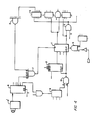
- Fig. 1 illustrating the application of the invention to digital circuits, a portion of a typical circuit under test is illustrated embodying three JK-type flip-flop components 1, 2, and 3, which, with two AND-gate components 4 and 5 form a divide-by-5 counting circuit.
- Fig. 1 does not show connectors between all circuit nodes and the testing apparatus in order to simplify the illustration.
- the first is due to the common clock signal on node 6 that is derived from a signal, SYSTEM CLOCK, operative during the test. This signal can interfere with the signal on node 6 applied by the test apparatus.
- the method of the invention suppresses such interference by driving or applying a low logic signal from the test apparatus to node 7 of gate 4 (ENABLE), thus inhibiting transfer of the SYSTEM CLOCK signal 8 to node 6.
- the second identified source of spurious signal is via a feedback path from the Q output of the flip-flop 1 under test, via node 9 to flip-flop 2 and gate 5. From node 9 the signal propagates through 2 and 5 to node 10, allowing flip-flop 3 to send a signal back to 1 via node 11.
- the fedback circuit signal on node 11 could interfere with test-apparatus signals on the same node.
- the method of the invention inhibits spurious pulses by applying overriding, driving or forcing low logic signals to flip-flop 3 at its J and K inputs, nodes 10 and 12. This would suppress state transitions of 3 and thus break or inhibit the feedback loop.
- An alternative technique for breaking the feedback loop would be to operate the circuit in such a manner as to place flip-flop 3 in its low-output (11) state, and then to inhibit further state change by applying a low state solely to node 13, the input of gate 5. This would require more circuit-analysis processing during automatic test generation, but would reduce the number of inhibit signals.
- the power of this technique is that it can be implemented automatically.
- the inhibit states can be added to the component test library normally used in developing all the in-circuit tests.
- the inhibit states do not, therefore, have to be identified each time a new circuit test is developed.
- the new test is merely assembled from the library using a computer program (ATG) which identified the components-to-be-inhibited as part of the assembly process.
- ATG computer program
- Automatic implementation is so efficient that inhibiting can be done as a matter of course, rather than on an as-required basis. This eliminates the labor intensive task of finding the cause of a failing test of a good component and implementing inhibiting.
- Inhibiting is applied in this embodiment to all inhibitable input paths to the component under test, regardless of their potential for being part of a source of spurious signal.
- the invention therefore makes it unnecessary to analyze the circuit for such sources, which is a complex activity, requires considerable computer power (memory) and is susceptible to error.
- FIG. 1 While shown applied to digital testing in Fig. 1, the underlying method of this form of the invention is-also useful for analog testing. An example is shown in Fig. 2, as combined with the circuit of Fig. 1, and which extends the operation for analog use.
- a digital-to-analog converter component 15 having digital inputs 9, 12 and 13 is shown connected to the Q outputs (Ql, Q2 and Q3) of the counter of Fig. 1.
- Normal circuit operation produces an analog output 14 that is a stepped wave-form 16.
- the analog test in this illustration consists of measuring the voltages at output 14 corresponding to digital input states at 9, 12 and 13.
- the testing apparatus would apply signals to these digital input nodes and conduct voltage measurements at 14. If, however, during the test, the circuit under test produced a clock signal on node 6, one or more of the flip-flop components could change state to produce a spurious signal at nodes 9, 12 or 13, resulting in a momentary error in output voltage 14. In accordance with the method of the invention, a low state would automatically be applied at node 6 to suppress such errors.
- this form of the invention (so-called second technique above-described) wherein some analysis is effected to identify all components that are capable of feeding or processing input signals to the component(s) under test and are thus potential components for the passing or conveying of spurious signals, and then automatically inhibiting all inhibitable spurious-signal input paths by specific driving signals to such identified components prior to or during the conduct of the test of the component(s) under test, resides in the requirement of less analysis and thus computer power than if only the actual paths that spurious signals can take are identified and only those paths are inhibited (so-called first technique above). Still, this latter technique is useful and, as memory becomes less expensive, is attractive in requiring fewer driver circuits and dealing, generally, with fewer than all possible inhibit signal nodes.
- the first gate in component 1, called “U25” in the test program combines two signals from device 2 (called “U17”) and device 3 (called “U8") onto a timing bus.
- the other gates in flip flop component 1 must be disabled. For this reason, nails 215, 227, 229, and 231 are driven low to disable these open collector gates.
- devices 2 and 3 are inhibited. For component 2, however, this requires only driving one line low, forcing it into its clear state.
- Putting component 3 into its "reset” (known inactive) state requires holding Reset high and clocking it eight times. After this has been done, device 1 may reliably be tested, since neither device 2 nor device 3 can pass spurious signals.
- Fig. 4 showing three spurious signal sources: first, a parallel signal through flip flop component 2, which shares a clock.line with flip flop component 1; second, a signal, from an independent clock device 3 1 ; and third, a feedback loop signal through gates 4, 5, 6, and 7.
- the many other devices, illustrated with conventional symbols, and other signals involved would make interference by these spurious signals intermittent and thus hard to diagnose or suppress. These signals are all suppressable by back- driving appropriate input pins.
- signal transmission may be suppressed on all devices that drive component 1; namely, devices 2, 7, 10, and 11.
Landscapes
- Engineering & Computer Science (AREA)
- General Engineering & Computer Science (AREA)
- Physics & Mathematics (AREA)
- General Physics & Mathematics (AREA)
- Tests Of Electronic Circuits (AREA)
Applications Claiming Priority (2)
| Application Number | Priority Date | Filing Date | Title |
|---|---|---|---|
| US06/373,809 US4555783A (en) | 1982-04-30 | 1982-04-30 | Method of computerized in-circuit testing of electrical components and the like with automatic spurious signal suppression |
| US373809 | 1982-04-30 |
Publications (2)
| Publication Number | Publication Date |
|---|---|
| EP0093531A2 true EP0093531A2 (de) | 1983-11-09 |
| EP0093531A3 EP0093531A3 (de) | 1986-02-19 |
Family
ID=23473966
Family Applications (1)
| Application Number | Title | Priority Date | Filing Date |
|---|---|---|---|
| EP83302171A Withdrawn EP0093531A3 (de) | 1982-04-30 | 1983-04-18 | Verfahren zum rechnergestützten "in-circuit"-Prüfen elektrischer Komponenten und dergleichen mit automatischer Nebensignalunterdrückung |
Country Status (3)
| Country | Link |
|---|---|
| US (1) | US4555783A (de) |
| EP (1) | EP0093531A3 (de) |
| JP (1) | JPH0664125B2 (de) |
Cited By (1)
| Publication number | Priority date | Publication date | Assignee | Title |
|---|---|---|---|---|
| GB2169087A (en) * | 1984-12-20 | 1986-07-02 | Int Computers Ltd | Testing electronic circuit assemblies including crystal oscillators |
Families Citing this family (6)
| Publication number | Priority date | Publication date | Assignee | Title |
|---|---|---|---|---|
| JPH0738187B2 (ja) * | 1984-03-23 | 1995-04-26 | 株式会社日立製作所 | Lsiに構成されたマイクロコンピュータ |
| GB2172403B (en) * | 1985-03-15 | 1988-11-02 | Membrain Ltd | Method for operating automatic test equipment |
| US4922492A (en) * | 1988-05-13 | 1990-05-01 | National Semiconductor Corp. | Architecture and device for testable mixed analog and digital VLSI circuits |
| US5392297A (en) * | 1989-04-18 | 1995-02-21 | Vlsi Technology, Inc. | Method for automatic isolation of functional blocks within integrated circuits |
| US5127009A (en) * | 1989-08-29 | 1992-06-30 | Genrad, Inc. | Method and apparatus for circuit board testing with controlled backdrive stress |
| US5321701A (en) * | 1990-12-06 | 1994-06-14 | Teradyne, Inc. | Method and apparatus for a minimal memory in-circuit digital tester |
Family Cites Families (4)
| Publication number | Priority date | Publication date | Assignee | Title |
|---|---|---|---|---|
| US3931506A (en) * | 1974-12-30 | 1976-01-06 | Zehntel, Inc. | Programmable tester |
| US4070565A (en) * | 1976-08-18 | 1978-01-24 | Zehntel, Inc. | Programmable tester method and apparatus |
| US4216539A (en) * | 1978-05-05 | 1980-08-05 | Zehntel, Inc. | In-circuit digital tester |
| US4236246A (en) * | 1978-11-03 | 1980-11-25 | Genrad, Inc. | Method of and apparatus for testing electronic circuit assemblies and the like |
-
1982
- 1982-04-30 US US06/373,809 patent/US4555783A/en not_active Expired - Fee Related
-
1983
- 1983-04-18 EP EP83302171A patent/EP0093531A3/de not_active Withdrawn
- 1983-04-27 JP JP58074875A patent/JPH0664125B2/ja not_active Expired - Lifetime
Non-Patent Citations (3)
| Title |
|---|
| ELECTRICAL DESIGN NEWS, vol. 27, no. 10, May 1982, pages 187-190, Boston, Massachusettes, US; M.W. SCHRAEDER: "Multiplexed measuring devices reduce in-circuit-test expenses" * |
| ELECTRONIC DESIGN, vol. 28, no. 21, October 1980, pages 191-195, Rochelle Park, US; A. NATRASEVSCHI: "SA attacks board faults without extra hardware" * |
| ELECTRONICS INTERNATIONAL, vol. 54, no. 25, December 1981, pages 146-150, New York, US; J. PRANG: "Board testing meets the challenges of ECL" * |
Cited By (1)
| Publication number | Priority date | Publication date | Assignee | Title |
|---|---|---|---|---|
| GB2169087A (en) * | 1984-12-20 | 1986-07-02 | Int Computers Ltd | Testing electronic circuit assemblies including crystal oscillators |
Also Published As
| Publication number | Publication date |
|---|---|
| EP0093531A3 (de) | 1986-02-19 |
| JPS58196470A (ja) | 1983-11-15 |
| JPH0664125B2 (ja) | 1994-08-22 |
| US4555783A (en) | 1985-11-26 |
Similar Documents
| Publication | Publication Date | Title |
|---|---|---|
| US4298980A (en) | LSI Circuitry conforming to level sensitive scan design (LSSD) rules and method of testing same | |
| US5291495A (en) | Method for designing a scan path for a logic circuit and testing of the same | |
| US4630270A (en) | Method for identifying a faulty cell in a chain of cells forming a shift register | |
| EP0140205A2 (de) | Methode und Vorrichtung für die Fehlerprüfung eines Taktverteilungsnetzwerks eines Prozessors | |
| JPH0481147B2 (de) | ||
| JP3262281B2 (ja) | 電子回路の試験方法と試験装置 | |
| US4555783A (en) | Method of computerized in-circuit testing of electrical components and the like with automatic spurious signal suppression | |
| US5365528A (en) | Method for testing delay faults in non-scan sequential circuits | |
| Abramovici et al. | WARNING: 100% fault coverage may be misleading!! | |
| US7500165B2 (en) | Systems and methods for controlling clock signals during scan testing integrated circuits | |
| US5898705A (en) | Method for detecting bus shorts in semiconductor devices | |
| US6105156A (en) | LSI tester for use in LSI fault analysis | |
| JPS61155874A (ja) | 大規模集積回路の故障検出方法およびそのための装置 | |
| US5623202A (en) | Testing multiple IC in parallel by a single IC tester | |
| EP0780037B1 (de) | Testverfahren für eine elektronische schaltung durch logisches verbinden von taktsignalen und elektronische schaltung mit vorrichtung für ein solches testverfahren | |
| US5590136A (en) | Method for creating an in-circuit test for an electronic device | |
| US5144229A (en) | Method for selectively conditioning integrated circuit outputs for in-circuit test | |
| US4686455A (en) | Method for the localization of time-critical events within a clock electronic circuit | |
| Rastogi et al. | A new approach to mixed-signal diagnosis | |
| JPH01156680A (ja) | 論理回路の故障診断方法 | |
| JP2773148B2 (ja) | テスト容易化回路設計方法 | |
| JP2501202B2 (ja) | 論理回路診断方法 | |
| Leet et al. | A CMOS LSSD test generation system | |
| Crook et al. | A computer controlled tester for logic networks and a method for synthesizing test patterns | |
| JPH0210178A (ja) | 論理回路 |
Legal Events
| Date | Code | Title | Description |
|---|---|---|---|
| PUAI | Public reference made under article 153(3) epc to a published international application that has entered the european phase |
Free format text: ORIGINAL CODE: 0009012 |
|
| AK | Designated contracting states |
Designated state(s): DE FR GB |
|
| RBV | Designated contracting states (corrected) |
Designated state(s): DE FR GB |
|
| PUAL | Search report despatched |
Free format text: ORIGINAL CODE: 0009013 |
|
| AK | Designated contracting states |
Designated state(s): DE FR GB |
|
| 17P | Request for examination filed |
Effective date: 19860805 |
|
| 17Q | First examination report despatched |
Effective date: 19880321 |
|
| STAA | Information on the status of an ep patent application or granted ep patent |
Free format text: STATUS: THE APPLICATION IS DEEMED TO BE WITHDRAWN |
|
| 18D | Application deemed to be withdrawn |
Effective date: 19890805 |
|
| RIN1 | Information on inventor provided before grant (corrected) |
Inventor name: SWANSON, MARK |