EP0091818A2 - Verfahren zur Herstellung eines Metalloxydmusters mit ebener Oberfläche - Google Patents
Verfahren zur Herstellung eines Metalloxydmusters mit ebener Oberfläche Download PDFInfo
- Publication number
- EP0091818A2 EP0091818A2 EP83302041A EP83302041A EP0091818A2 EP 0091818 A2 EP0091818 A2 EP 0091818A2 EP 83302041 A EP83302041 A EP 83302041A EP 83302041 A EP83302041 A EP 83302041A EP 0091818 A2 EP0091818 A2 EP 0091818A2
- Authority
- EP
- European Patent Office
- Prior art keywords
- layer
- cavity
- portions
- side walls
- aluminum
- Prior art date
- Legal status (The legal status is an assumption and is not a legal conclusion. Google has not performed a legal analysis and makes no representation as to the accuracy of the status listed.)
- Granted
Links
- 238000000034 method Methods 0.000 title claims abstract description 43
- 238000004519 manufacturing process Methods 0.000 title claims abstract description 7
- 229910044991 metal oxide Inorganic materials 0.000 title abstract description 6
- 150000004706 metal oxides Chemical class 0.000 title abstract description 6
- 230000008569 process Effects 0.000 title description 2
- 239000000463 material Substances 0.000 claims abstract description 57
- 239000000758 substrate Substances 0.000 claims abstract description 20
- 239000010409 thin film Substances 0.000 claims abstract description 19
- 229910052782 aluminium Inorganic materials 0.000 claims description 50
- XAGFODPZIPBFFR-UHFFFAOYSA-N aluminium Chemical compound [Al] XAGFODPZIPBFFR-UHFFFAOYSA-N 0.000 claims description 49
- VYPSYNLAJGMNEJ-UHFFFAOYSA-N Silicium dioxide Chemical compound O=[Si]=O VYPSYNLAJGMNEJ-UHFFFAOYSA-N 0.000 claims description 30
- 229910052751 metal Inorganic materials 0.000 claims description 18
- 239000002184 metal Substances 0.000 claims description 18
- 238000007743 anodising Methods 0.000 claims description 14
- 239000000377 silicon dioxide Substances 0.000 claims description 14
- 238000000151 deposition Methods 0.000 claims description 9
- 239000007769 metal material Substances 0.000 claims description 8
- PNEYBMLMFCGWSK-UHFFFAOYSA-N aluminium oxide Inorganic materials [O-2].[O-2].[O-2].[Al+3].[Al+3] PNEYBMLMFCGWSK-UHFFFAOYSA-N 0.000 claims description 7
- 230000008021 deposition Effects 0.000 claims description 7
- 229920002120 photoresistant polymer Polymers 0.000 claims description 7
- 229910052681 coesite Inorganic materials 0.000 claims description 6
- 229910052906 cristobalite Inorganic materials 0.000 claims description 6
- 229910052682 stishovite Inorganic materials 0.000 claims description 6
- 229910052905 tridymite Inorganic materials 0.000 claims description 6
- 238000001020 plasma etching Methods 0.000 claims description 5
- 238000004544 sputter deposition Methods 0.000 claims description 5
- 239000011651 chromium Substances 0.000 claims description 4
- 229910052593 corundum Inorganic materials 0.000 claims description 4
- 229910001845 yogo sapphire Inorganic materials 0.000 claims description 4
- 229910003271 Ni-Fe Inorganic materials 0.000 claims description 3
- VYZAMTAEIAYCRO-UHFFFAOYSA-N Chromium Chemical compound [Cr] VYZAMTAEIAYCRO-UHFFFAOYSA-N 0.000 claims description 2
- 229910052581 Si3N4 Inorganic materials 0.000 claims description 2
- 229910052804 chromium Inorganic materials 0.000 claims description 2
- GNFTZDOKVXKIBK-UHFFFAOYSA-N 3-(2-methoxyethoxy)benzohydrazide Chemical compound COCCOC1=CC=CC(C(=O)NN)=C1 GNFTZDOKVXKIBK-UHFFFAOYSA-N 0.000 claims 1
- 238000010894 electron beam technology Methods 0.000 claims 1
- 230000008016 vaporization Effects 0.000 claims 1
- 238000009834 vaporization Methods 0.000 claims 1
- 239000000945 filler Substances 0.000 abstract description 4
- 230000000873 masking effect Effects 0.000 abstract description 4
- 229910000765 intermetallic Inorganic materials 0.000 abstract description 3
- 238000005530 etching Methods 0.000 abstract description 2
- 229910000889 permalloy Inorganic materials 0.000 description 26
- 239000000696 magnetic material Substances 0.000 description 17
- 235000012239 silicon dioxide Nutrition 0.000 description 10
- HEMHJVSKTPXQMS-UHFFFAOYSA-M Sodium hydroxide Chemical compound [OH-].[Na+] HEMHJVSKTPXQMS-UHFFFAOYSA-M 0.000 description 9
- TWNQGVIAIRXVLR-UHFFFAOYSA-N oxo(oxoalumanyloxy)alumane Chemical compound O=[Al]O[Al]=O TWNQGVIAIRXVLR-UHFFFAOYSA-N 0.000 description 8
- 238000004804 winding Methods 0.000 description 8
- NBIIXXVUZAFLBC-UHFFFAOYSA-N Phosphoric acid Chemical compound OP(O)(O)=O NBIIXXVUZAFLBC-UHFFFAOYSA-N 0.000 description 4
- 150000001875 compounds Chemical class 0.000 description 3
- 239000011521 glass Substances 0.000 description 3
- 230000003647 oxidation Effects 0.000 description 3
- 238000007254 oxidation reaction Methods 0.000 description 3
- 229910000147 aluminium phosphate Inorganic materials 0.000 description 2
- 230000000694 effects Effects 0.000 description 2
- 238000005566 electron beam evaporation Methods 0.000 description 2
- 239000010408 film Substances 0.000 description 2
- 239000012762 magnetic filler Substances 0.000 description 2
- 238000000992 sputter etching Methods 0.000 description 2
- 229910001030 Iron–nickel alloy Inorganic materials 0.000 description 1
- 230000004888 barrier function Effects 0.000 description 1
- 230000008901 benefit Effects 0.000 description 1
- 230000015572 biosynthetic process Effects 0.000 description 1
- 238000003486 chemical etching Methods 0.000 description 1
- 239000011231 conductive filler Substances 0.000 description 1
- 239000004020 conductor Substances 0.000 description 1
- 238000010276 construction Methods 0.000 description 1
- 238000009792 diffusion process Methods 0.000 description 1
- 230000003292 diminished effect Effects 0.000 description 1
- 230000001939 inductive effect Effects 0.000 description 1
- UGKDIUIOSMUOAW-UHFFFAOYSA-N iron nickel Chemical compound [Fe].[Ni] UGKDIUIOSMUOAW-UHFFFAOYSA-N 0.000 description 1
- 239000000203 mixture Substances 0.000 description 1
- 238000012986 modification Methods 0.000 description 1
- 230000004048 modification Effects 0.000 description 1
- 230000005855 radiation Effects 0.000 description 1
- 238000001552 radio frequency sputter deposition Methods 0.000 description 1
- -1 silicon dioxide Chemical class 0.000 description 1
- 230000007704 transition Effects 0.000 description 1
Images
Classifications
-
- H—ELECTRICITY
- H01—ELECTRIC ELEMENTS
- H01F—MAGNETS; INDUCTANCES; TRANSFORMERS; SELECTION OF MATERIALS FOR THEIR MAGNETIC PROPERTIES
- H01F41/00—Apparatus or processes specially adapted for manufacturing or assembling magnets, inductances or transformers; Apparatus or processes specially adapted for manufacturing materials characterised by their magnetic properties
- H01F41/32—Apparatus or processes specially adapted for manufacturing or assembling magnets, inductances or transformers; Apparatus or processes specially adapted for manufacturing materials characterised by their magnetic properties for applying conductive, insulating or magnetic material on a magnetic film, specially adapted for a thin magnetic film
- H01F41/34—Apparatus or processes specially adapted for manufacturing or assembling magnets, inductances or transformers; Apparatus or processes specially adapted for manufacturing materials characterised by their magnetic properties for applying conductive, insulating or magnetic material on a magnetic film, specially adapted for a thin magnetic film in patterns, e.g. by lithography
-
- G—PHYSICS
- G11—INFORMATION STORAGE
- G11B—INFORMATION STORAGE BASED ON RELATIVE MOVEMENT BETWEEN RECORD CARRIER AND TRANSDUCER
- G11B5/00—Recording by magnetisation or demagnetisation of a record carrier; Reproducing by magnetic means; Record carriers therefor
- G11B5/127—Structure or manufacture of heads, e.g. inductive
- G11B5/31—Structure or manufacture of heads, e.g. inductive using thin films
- G11B5/3163—Fabrication methods or processes specially adapted for a particular head structure, e.g. using base layers for electroplating, using functional layers for masking, using energy or particle beams for shaping the structure or modifying the properties of the basic layers
Definitions
- the subject invention relates to the fabrication of metal oxide patterns on a substrate adapted for use with thin film inductive transducers.
- the transducers commonly referred to as thin film magnetic heads, are useful for recording and reading magnetic transitions on a moving magnetic recording medium.
- Thin film recording heads are generally manufactured by an etching process wherein an electromagnet is formed on the surface of a substrate. More particularly, a magnetic material is deposited on a suitable substrate and is etched to the desired configuration. Thereafter, conductive layers are deposited on the magnetic material and etched to define the windings of the electromagnet. At least one additional layer of magnetic material is deposited in a manner such that the rear ends of the magnetic materials are connected while the front ends thereof are separated to define a recording gap. An electric current may be passed through the windings of the conductor for recording.
- the gap or pole tip region of the head is intended to fly in close proximity to the magnetic recording medium.
- it is of critical importance to define the geometry of the pole tip region to within extremely precise tolerances. It has been found that read/write errors can be minimized when the pole tip regions of the electromagnet are formed with straight side walls.
- the side walls of the remaining portions of the magnetic head need not be formed with a precise vertical geometry.
- problems arise relating to the deposition of the conductive layer used to define the windings of the electromagnet.
- windings deposited on the magnetic material will frequently have undesirable discontinuities particularly in regions having sharp corners.
- planarization includes filling in the areas, adjacent the magnetic material, with a non-magnetic, non-metallic compound in a manner such that the top surface of the resulting structure is defined by a smooth plane.
- the magnetic material is formed with vertical side walls throughout its construction. Further, since the upper surface of the magnetic material is co-planar with the non-magnetic filler material, additional layers may be accurately deposited on the planar surface of the structure whereby discontinuities may be substantially diminished.
- thermal oxidation is a diffusion process which typically takes place at elevated temperatures in the range of 950 to 1200 degrees centigrade. This method is not adaptable to present manufacuring requirements since the materials utilized in forming the thin film magnetic heads suffer severe degreda- tion, including recrystalization and strain, when subjected to temperatures over 400 degrees centigrade.
- Another possible method includes the use of liquified glasses, which can be flowably formed on the substrate. However, as with thermal oxidation, most usable glasses melt at temperatures greater than 400 degrees centigrade. The glasses which are found to melt at lower temperatures are not compatible with thin film processing because their thermal expansion and softening points are not satisfactory. Accordingly, it would be desirable to provide a new and improved method for planarizing the surface of the magnetic material of a thin film recording head such that successive layers may be readily deposited without discontinuities.
- the subject invention relates to a method of fabricating the metallic magnetic pattern on a substrate for use with thin film recording heads.
- the metallic pattern and non-magnetic, non-conductive filler material are formed on the substrate in complimentary patterns such that the top surfaces of both materials are co-planar.
- a relatively thinner second layer is deposited over the non-magnetic layer.
- the second layer is formed from a metal such as aluminum or chromium which is insoluable in a silicon dioxide etchant.
- a photoresist layer is placed on the top of the metal layer in a negative pattern with respect to the desired metallic magnetic pattern.
- the silicon dioxide layer is plasma etched to define a cavity having a configuration corresponding to the desired metallic pattern. Due to the high speed and directional nature of plasma etching, a cavity having relatively vertical side walls is produced. After the plasma etching step, any remaining portions of the aluminum layer are removed. If Al203 is used Cr is the desired masking material and the Al203 can be etched in a mixture of HN0 3 , HF and H 2 0. The A1 2 0 3 can be deposited with RF sputtering or reactive oxide sputtering and the deposition parameters are choosen to enhance the etch rate and form nearly vertical side walls.
- the deposited aluminum layer is soft anodized to a depth sufficient to affect all of the aluminum formed on the side walls of the cavity.
- the base of the cavity is electrically connected in a circuit and the anodizing step is continued until the aluminum on the side walls is converted and the circuit is broken.
- the soft anodized portions of the aluminum are then removed by an etchant which does not attack either the unchanged aluminum or the dielectric.
- the aluminum located on top of the SiO 2 layer is hard anodized. This is accomplished electrochemically by linking the aluminum on the top portions in a circuit. Since the aluminum in the bottom of the cavity is electrically isolated from the aluminum on the top surface of the Si0 2 , only latter will be hard anodized. Using the hard anodized aluminum as a mask, the remaining aluminum in the cavity can be etched using a phosphoric acid based solution.
- a layer of the magnetic metallic material is applied to the structure.
- a Ni-Fe permalloy material is used.
- the permalloy is applied such that the cavity is filled while a relatively thin layer is formed adjacent the upper edges of the cavity.
- the upper surface of the permalloy is then removed to a depth sufficient to expose the aluminum layer adjacent the top edges of the cavity.
- the removal of the permalloy can be accomplished through well known sputter etching techniques.
- the structure can be emersed in a bath of sodium hydroxide which functions to dissolve the aluminum.
- the removal of the intermediate aluminum layer functions to strip the excess permalloy from the structure resulting in a configuration wherein the cavity is filled, while the top surface of the permalloy is co-planar with the SiO 2 layer. Accordingly, subsequent layers, including the conductive windings may be readily applied to the planarized structure. Further, the permalloy is formed with vertical, or nearly vertical straight side walls for maximizing read/write operations.
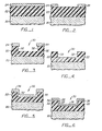
- Figure 1 is side elevational view illustrating a substrate having layers formed thereon in accordance with the initial steps of the subject method.
- Figures 2-10 are side elevational views, similar to Figure 1, illustrating subsequent steps of the new and improved method of the subject invention.
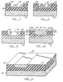
- Figure 11 is a partial perspective view,of the structure including the bottom pole of a thin film recording head, made in accordance with the method of the subject invention.
- the subject invention relates to a method for fabricating a metallic magnetic pattern on a substrate.
- the magnetic metallic pattern formed from Ni-Fe permalloy material, defines the bottom pole of a thin film transducer.
- Figures 1-10 illustrate the steps of the subject method.
- Thin film magnetic heads are formed on a non-magnetic substrate 20. Typically, a plurality of magnetic recording heads will be placed in a spaced array, along the length of the substrate 20.
- a first layer of filler material 22 is applied to the substrate to a depth somewhat thicker than the desired thickness of the eventual permalloy pattern, which generally ranges from approximately 3-4 microns.
- the filler material 22 is formed from a non-conductive, non-metallic compound such as silicon dioxide. Other possible compounds include Si 3 N 4 and A 1 2 0 3 .
- a relatively thinner, second metal layer 24 is applied.
- the particular metal of the second layer 24 is selected to have good' adhesion to the first layer material and to be insoluable in an etchant which will attack the first material.
- the metal 24 of the second layer is aluminum if Sio 2 is the first layer and Cr if Al 2 0 3 is the first layer and has a thickness on the order of approximately .1 to 1 microns.
- a layer (not shown) of photoresist material is applied to the upper surface of the metal layer 24.
- the photoresist must be etched to define a negative pattern, complimentary to the desired pattern of the permalloy. Typically, this is accomplished using a masking technique wherein the photoresist is selectively exposed to curing radiation. The non-cured portion may then be removed to define the negative pattern.
- a suitable etchant for metal is then applied to the surface of the structure for removing the portions of the second aluminum layer 24 not masked by the remaining photoresist to achieve the configuration illustrated in Figure 2.
- the layer 22 is then etched to define a cavity 30, having relatively vertical side walls 32 as illustrated in Figure 3.
- side walls 32 of cavity 30 serve to define the desired side walls of the permalloy material.
- the silicon dioxide layer 22 is plasma etched, using the upper aluminum layer 24 as a mask. Plasma etching is a relatively high speed, directional operation which can provide the accuracy necessary for this removal step.
- the remaining layer 24 is removed to achieve the structure illustrated.in' Figure 4.
- the photoresist layer may be removed either prior to, or after the plasma etching step. When layer 24 is aluminum, it can be most readily removed by chemical etching.
- another metal layer 36 is formed on the structure by, for example, electron beam evaporation.
- the metal is preferably aluminum.
- layer 36 is not applied uniformly. More particularly, the thickness of the metal layer 36 is greater on the horizontal surfaces than along the vertical side walls 32 of the cavity 30.
- a non-uniform layer which is commonly formed over angular structures, was considered a shortcoming, since it often resulted in undesirable discontinuities in the layer.
- this effect is used advantageously in the subject invention.
- the thickness of the metal layer 36, along the horizontal surfaces of the structure is about twice as great as the thickness along the side walls 32 thereof.
- the aluminum layer 36 is then subjected to a soft anodizing step to form a thin porous alumina (aluminum oxide) film 38 on its surface.
- a soft anodizing step to form a thin porous alumina (aluminum oxide) film 38 on its surface.
- the method and apparatus used for anodizing are well known in the art and need not be described in detail. Briefly, the structure is submersed in a electrolytic anodizing solution and a potential is supplied between the aluminum layer and the solution. The anodizing step is continued to a depth sufficient to convert all of the aluminum on the side walls 32 of the cavity to aluminum oxide. This result may be readily achieved because the electrical current will continue to flow through the conductive aluminum until the metal on the side walls has been converted to non-conductive, aluminum oxide. The length of time this step takes is a function of the thickness of the layer as well as the strength of the current supplied. The structure produced after this step is illustrated in Figure 6.
- the aluminum oxide film 38 is dissolved.
- a suitable etchant is chosen which does not attack either the remaining aluminum layer 36 or the Si0 2 layer 22.
- the result of this dissolving step is to isolate the aluminum 36A in the base of the cavity 30 from the aluminum 36B remaining on the upper surface of the silicon dioxide layer 22 as illustrated in Figure 7.
- the upper surface of the aluminum portions 36B, on the top surface of the silicon dioxide layer 22, may then be hard anodized.
- Hard anodizing forms a non-porous or barrier alumina layer, as compared with the porous layer formed in the soft anodizing step.
- the hard anodizing step is carried out electrochemically wherein a bus is connected only to the aluminum portions 36B, located on the top surface of the silicon dioxide layer 22. Since the aluminum 36A disposed at the base of the cavity 30 is electrically isolated from the remaining aluminum 36B, only the latter portions will be anodized into alumina 40, as illustrated in Figure 8.
- the aluminum 36A, remaining in the cavity 30 is removed, as illustrated in Figure 9.
- the hard anodized aluminua layer 40 masks the aluminum 36B underneath.
- the etchant is chosen such that it will not attack the silicon dioxide layer 22.
- Cavity 30 may then be filled with the desired magnetic metallic material.
- the magnetic material is formed from a nickel-iron or permalloy compound.
- the permalloy layer 42 can be formed utilizing well known sputtering techniques. As illustrated in Figure 10, the cavity 30 is filled while a relatively thin layer is defined adjacent the top edges 44 of the cavity. As can be appreciated, since the cavity 30 is defined with accurate, vertical side walls, the permalloy in the cavity will be formed with similar, complimentary vertical sidewalls.
- the permalloy layer 42 is then removed in a manner to expose the aluminum layer 36B adjacent the top edges 44 of the cavity 30.
- the removal of the permalloy is accomplished by a back sputtering or sputter etching technique.
- aluminum layer 36B may be dissolved to release the excess permalloy 42.
- the structure is emersed in a sodium hydroxide solution, which is capable of dissolving both aluminum and aluminum oxide.
- the sodium hydroxide solution will dissolve either aluminum or the aluminum oxide such that the aluminum oxide layer 40 may be removed during this step.
- the aluminum oxide layer 40 can be removed prior to the addition of the permalloy layer 42.
- planarized structure is uniquely suited for the production of thin film magnetic heads. More particularly, since the side walls 32 of the permalloy material 42 are provided with accurate vertical side walls, the reading and writing ability of a recording head produced therefrom is maximized. In addition, the upper surface of the permalloy 42 is co-planar with the upper surface of the silicon dioxide layer 22. By this arrangement, additional layers may be uniformly deposited on the upper planar surface of the structure such that discontinuities, prevalent in the prior art, are substantially reduced.
- a new and improved method for producing metallic magnetic patterns on a substrate for use with thin film magnetic recording heads In the subject method, a permalloy pattern 42 is formed on the substrate. 'A non-magnetic, non-metallic material 22 is filled in around the side edges of the permalloy such that the top surface of the structure defines a plane.
- additional layers may be readily deposited on the structure, while a permalloy pattern is defined which satisfies the strict geometric tolerance requirements necessary for accurate read/write operations.
Landscapes
- Engineering & Computer Science (AREA)
- Manufacturing & Machinery (AREA)
- Power Engineering (AREA)
- Magnetic Heads (AREA)
Applications Claiming Priority (2)
| Application Number | Priority Date | Filing Date | Title |
|---|---|---|---|
| US06/367,366 US4391849A (en) | 1982-04-12 | 1982-04-12 | Metal oxide patterns with planar surface |
| US367366 | 1982-04-12 |
Publications (3)
| Publication Number | Publication Date |
|---|---|
| EP0091818A2 true EP0091818A2 (de) | 1983-10-19 |
| EP0091818A3 EP0091818A3 (en) | 1986-02-05 |
| EP0091818B1 EP0091818B1 (de) | 1988-06-15 |
Family
ID=23446876
Family Applications (1)
| Application Number | Title | Priority Date | Filing Date |
|---|---|---|---|
| EP83302041A Expired EP0091818B1 (de) | 1982-04-12 | 1983-04-12 | Verfahren zur Herstellung eines Metalloxydmusters mit ebener Oberfläche |
Country Status (5)
| Country | Link |
|---|---|
| US (1) | US4391849A (de) |
| EP (1) | EP0091818B1 (de) |
| CA (1) | CA1193479A (de) |
| DE (1) | DE3377095D1 (de) |
| WO (1) | WO1983003711A1 (de) |
Families Citing this family (14)
| Publication number | Priority date | Publication date | Assignee | Title |
|---|---|---|---|---|
| FR2741470B1 (fr) * | 1995-11-22 | 1998-01-02 | Commissariat Energie Atomique | Procede de realisation d'une tete magnetique planaire et tete obtenue par ce procede |
| US4517616A (en) * | 1982-04-12 | 1985-05-14 | Memorex Corporation | Thin film magnetic recording transducer having embedded pole piece design |
| FR2539556B1 (fr) * | 1983-01-13 | 1986-03-28 | Commissariat Energie Atomique | Procede de fabrication de conducteurs pour circuits integres, en technologie planar |
| US4600445A (en) * | 1984-09-14 | 1986-07-15 | International Business Machines Corporation | Process for making self aligned field isolation regions in a semiconductor substrate |
| US5159511A (en) * | 1987-04-01 | 1992-10-27 | Digital Equipment Corporation | Biasing conductor for MR head |
| US5162191A (en) * | 1988-01-05 | 1992-11-10 | Max Levy Autograph, Inc. | High-density circuit and method of its manufacture |
| US5488394A (en) * | 1988-01-05 | 1996-01-30 | Max Levy Autograph, Inc. | Print head and method of making same |
| US4897676A (en) * | 1988-01-05 | 1990-01-30 | Max Levy Autograph, Inc. | High-density circuit and method of its manufacture |
| EP0351048A3 (de) * | 1988-07-11 | 1992-04-08 | Digital Equipment Corporation | Aufzeichnungskopf zum optimieren der Aufzeichnung hoher Dichte |
| US5068959A (en) * | 1988-07-11 | 1991-12-03 | Digital Equipment Corporation | Method of manufacturing a thin film head |
| US5350618A (en) * | 1991-03-01 | 1994-09-27 | Teijin Seiki Co., Ltd. | Magnetic medium comprising a substrate having pits and grooves of specific shapes and depths |
| US5242534A (en) * | 1992-09-18 | 1993-09-07 | Radiant Technologies | Platinum lift-off process |
| US5831801A (en) * | 1997-01-21 | 1998-11-03 | Yamaha Corporation | Thin film magnetic head with special pole configuration |
| US6375063B1 (en) * | 1999-07-16 | 2002-04-23 | Quantum Corporation | Multi-step stud design and method for producing closely packed interconnects in magnetic recording heads |
Family Cites Families (23)
| Publication number | Priority date | Publication date | Assignee | Title |
|---|---|---|---|---|
| US3672043A (en) * | 1965-12-06 | 1972-06-27 | Ncr Co | Miniature magnetic head |
| US3741880A (en) * | 1969-10-25 | 1973-06-26 | Nippon Electric Co | Method of forming electrical connections in a semiconductor integrated circuit |
| BE758053A (fr) * | 1969-10-28 | 1971-04-01 | Commissariat Energie Atomique | Tete magnetique integree et procede de fabrication de ladite tete |
| US3708403A (en) * | 1971-09-01 | 1973-01-02 | L Terry | Self-aligning electroplating mask |
| US3939047A (en) * | 1971-11-15 | 1976-02-17 | Nippon Electric Co., Ltd. | Method for fabricating electrode structure for a semiconductor device having a shallow junction |
| US3969746A (en) * | 1973-12-10 | 1976-07-13 | Texas Instruments Incorporated | Vertical multijunction solar cell |
| US4005452A (en) * | 1974-11-15 | 1977-01-25 | International Telephone And Telegraph Corporation | Method for providing electrical isolating material in selected regions of a semiconductive material and the product produced thereby |
| JPS588579B2 (ja) * | 1975-08-20 | 1983-02-16 | 松下電器産業株式会社 | ハンドウタイソウチノセイゾウホウホウ |
| US4052749A (en) * | 1976-05-19 | 1977-10-04 | Matsushita Electric Industrial Co., Ltd. | Thin film magnetic head |
| US4076575A (en) * | 1976-06-30 | 1978-02-28 | International Business Machines Corporation | Integrated fabrication method of forming connectors through insulative layers |
| US4045302A (en) * | 1976-07-08 | 1977-08-30 | Burroughs Corporation | Multilevel metallization process |
| DE2658400A1 (de) * | 1976-12-23 | 1978-06-29 | Ibm Deutschland | Verfahren zur herstellung einer negativen maske auf einem substrat |
| US4069094A (en) * | 1976-12-30 | 1978-01-17 | Rca Corporation | Method of manufacturing apertured aluminum oxide substrates |
| US4206541A (en) * | 1978-06-26 | 1980-06-10 | Extel Corporation | Method of manufacturing thin film thermal print heads |
| US4275286A (en) * | 1978-12-04 | 1981-06-23 | Hughes Aircraft Company | Process and mask for ion beam etching of fine patterns |
| US4161430A (en) * | 1978-12-04 | 1979-07-17 | Burroughs Corporation | Method of forming integrated circuit metal interconnect structure employing molybdenum on aluminum |
| US4199384A (en) * | 1979-01-29 | 1980-04-22 | Rca Corporation | Method of making a planar semiconductor on insulating substrate device utilizing the deposition of a dual dielectric layer between device islands |
| EP0022580A1 (de) * | 1979-07-17 | 1981-01-21 | Western Electric Company, Incorporated | Herstellungsverfahren von auf magnetische Eigenschaften basierten Vorrichtungen |
| US4334950A (en) * | 1979-07-17 | 1982-06-15 | Bell Telephone Laboratories, Incorporated | Advantageous fabrication technique for devices relying on magnetic properties |
| US4251319A (en) * | 1979-12-21 | 1981-02-17 | Control Data Corporation | Bubble memory chip and method for manufacture |
| US4317700A (en) * | 1980-08-20 | 1982-03-02 | Rockwell International Corporation | Method of fabrication of planar bubble domain device structures |
| JPS5823316A (ja) * | 1981-08-04 | 1983-02-12 | Matsushita Electric Ind Co Ltd | 薄膜磁気ヘツドの製造方法 |
| DE3132452A1 (de) * | 1981-08-17 | 1983-02-24 | Siemens AG, 1000 Berlin und 8000 München | Verfahren zum herstellen einer nach dem galvanischen aufbau von metallischen strukturen planaren strukturebene |
-
1982
- 1982-04-12 US US06/367,366 patent/US4391849A/en not_active Expired - Lifetime
-
1983
- 1983-04-11 CA CA000425627A patent/CA1193479A/en not_active Expired
- 1983-04-12 DE DE8383302041T patent/DE3377095D1/de not_active Expired
- 1983-04-12 EP EP83302041A patent/EP0091818B1/de not_active Expired
- 1983-04-12 WO PCT/US1983/000521 patent/WO1983003711A1/en not_active Ceased
Also Published As
| Publication number | Publication date |
|---|---|
| EP0091818A3 (en) | 1986-02-05 |
| WO1983003711A1 (en) | 1983-10-27 |
| EP0091818B1 (de) | 1988-06-15 |
| US4391849A (en) | 1983-07-05 |
| CA1193479A (en) | 1985-09-17 |
| DE3377095D1 (en) | 1988-07-21 |
Similar Documents
| Publication | Publication Date | Title |
|---|---|---|
| US4517616A (en) | Thin film magnetic recording transducer having embedded pole piece design | |
| US4391849A (en) | Metal oxide patterns with planar surface | |
| US5141623A (en) | Method for aligning pole tips in a thin film head | |
| US5820770A (en) | Thin film magnetic head including vias formed in alumina layer and process for making the same | |
| US4436593A (en) | Self-aligned pole tips | |
| US4624048A (en) | Method of making magnetic head sliders | |
| US5200056A (en) | Method for aligning pole tips in a thin film head | |
| US4239587A (en) | Method of manufacturing a thin-film magnetic head with a nickel-iron pattern having inclined edges | |
| JPH0916908A (ja) | 薄膜磁気コアコイル組立体 | |
| US4402801A (en) | Method for manufacturing thin film magnetic head | |
| JPH03105712A (ja) | 薄膜層にオーディオ、ビデオ及びコンピュータ用磁気ヘッドのポール・ピース及びギャップを形成する方法 | |
| US6167611B1 (en) | Process for producing a vertical magnetic head | |
| US5700381A (en) | Method for manufacturing thin film magnetic head | |
| US5695656A (en) | Method for fabricating a magnetic thin-film head | |
| US20050177996A1 (en) | Perpendicular magnetic pole structure and process | |
| US4178635A (en) | Planar and near planar magnetic bubble circuits | |
| JP2588392B2 (ja) | 薄膜磁気ヘツドの製造方法 | |
| JPH0150006B2 (de) | ||
| US4334950A (en) | Advantageous fabrication technique for devices relying on magnetic properties | |
| US4214960A (en) | Method of electrolytically etching ferrite | |
| EP0022580A1 (de) | Herstellungsverfahren von auf magnetische Eigenschaften basierten Vorrichtungen | |
| JPH0227508A (ja) | 薄膜磁気ヘッドの製造方法 | |
| JPS61120329A (ja) | ヘツドスライダの製造方法 | |
| US4280195A (en) | Planar and near planar magnetic bubble circuits | |
| JPS643337B2 (de) |
Legal Events
| Date | Code | Title | Description |
|---|---|---|---|
| PUAI | Public reference made under article 153(3) epc to a published international application that has entered the european phase |
Free format text: ORIGINAL CODE: 0009012 |
|
| 17P | Request for examination filed |
Effective date: 19830418 |
|
| AK | Designated contracting states |
Designated state(s): BE DE FR GB NL SE |
|
| PUAL | Search report despatched |
Free format text: ORIGINAL CODE: 0009013 |
|
| AK | Designated contracting states |
Designated state(s): BE DE FR GB NL SE |
|
| 17Q | First examination report despatched |
Effective date: 19870202 |
|
| GRAA | (expected) grant |
Free format text: ORIGINAL CODE: 0009210 |
|
| AK | Designated contracting states |
Kind code of ref document: B1 Designated state(s): BE DE FR GB NL SE |
|
| REF | Corresponds to: |
Ref document number: 3377095 Country of ref document: DE Date of ref document: 19880721 |
|
| ET | Fr: translation filed | ||
| BECN | Be: change of holder's name |
Effective date: 19880615 |
|
| NLS | Nl: assignments of ep-patents |
Owner name: UNISYS CORPORATION TE BLUE BELL, PENNSYLVANIE, VER |
|
| NLT1 | Nl: modifications of names registered in virtue of documents presented to the patent office pursuant to art. 16 a, paragraph 1 |
Owner name: UNISYS PERIPHERALS CORPORATION TE SANTA CLARA, CAL |
|
| PLBE | No opposition filed within time limit |
Free format text: ORIGINAL CODE: 0009261 |
|
| STAA | Information on the status of an ep patent application or granted ep patent |
Free format text: STATUS: NO OPPOSITION FILED WITHIN TIME LIMIT |
|
| 26N | No opposition filed | ||
| REG | Reference to a national code |
Ref country code: FR Ref legal event code: TP Ref country code: FR Ref legal event code: CD |
|
| REG | Reference to a national code |
Ref country code: GB Ref legal event code: 732 |
|
| BECH | Be: change of holder |
Free format text: 881222 *UNISYS CORP. |
|
| PGFP | Annual fee paid to national office [announced via postgrant information from national office to epo] |
Ref country code: SE Payment date: 19920319 Year of fee payment: 10 |
|
| PGFP | Annual fee paid to national office [announced via postgrant information from national office to epo] |
Ref country code: BE Payment date: 19920512 Year of fee payment: 10 |
|
| PGFP | Annual fee paid to national office [announced via postgrant information from national office to epo] |
Ref country code: FR Payment date: 19930412 Year of fee payment: 11 |
|
| PG25 | Lapsed in a contracting state [announced via postgrant information from national office to epo] |
Ref country code: SE Effective date: 19930413 |
|
| PG25 | Lapsed in a contracting state [announced via postgrant information from national office to epo] |
Ref country code: BE Effective date: 19930430 |
|
| BERE | Be: lapsed |
Owner name: UNISYS CORP. Effective date: 19930430 |
|
| PGFP | Annual fee paid to national office [announced via postgrant information from national office to epo] |
Ref country code: DE Payment date: 19940427 Year of fee payment: 12 |
|
| PGFP | Annual fee paid to national office [announced via postgrant information from national office to epo] |
Ref country code: NL Payment date: 19940430 Year of fee payment: 12 |
|
| PG25 | Lapsed in a contracting state [announced via postgrant information from national office to epo] |
Ref country code: FR Effective date: 19941229 |
|
| EUG | Se: european patent has lapsed |
Ref document number: 83302041.5 Effective date: 19931110 |
|
| REG | Reference to a national code |
Ref country code: FR Ref legal event code: ST |
|
| PG25 | Lapsed in a contracting state [announced via postgrant information from national office to epo] |
Ref country code: NL Effective date: 19951101 |
|
| NLV4 | Nl: lapsed or anulled due to non-payment of the annual fee |
Effective date: 19951101 |
|
| PG25 | Lapsed in a contracting state [announced via postgrant information from national office to epo] |
Ref country code: DE Effective date: 19960103 |
|
| PGFP | Annual fee paid to national office [announced via postgrant information from national office to epo] |
Ref country code: GB Payment date: 20000317 Year of fee payment: 18 |
|
| PG25 | Lapsed in a contracting state [announced via postgrant information from national office to epo] |
Ref country code: GB Free format text: LAPSE BECAUSE OF NON-PAYMENT OF DUE FEES Effective date: 20010412 |
|
| GBPC | Gb: european patent ceased through non-payment of renewal fee |
Effective date: 20010412 |