EP0090638B1 - Système à mémoire-antémémoire - Google Patents
Système à mémoire-antémémoire Download PDFInfo
- Publication number
- EP0090638B1 EP0090638B1 EP83301749A EP83301749A EP0090638B1 EP 0090638 B1 EP0090638 B1 EP 0090638B1 EP 83301749 A EP83301749 A EP 83301749A EP 83301749 A EP83301749 A EP 83301749A EP 0090638 B1 EP0090638 B1 EP 0090638B1
- Authority
- EP
- European Patent Office
- Prior art keywords
- level
- cache memory
- signal
- cache
- levels
- Prior art date
- Legal status (The legal status is an assumption and is not a legal conclusion. Google has not performed a legal analysis and makes no representation as to the accuracy of the status listed.)
- Expired
Links
Images

Classifications
-
- G—PHYSICS
- G11—INFORMATION STORAGE
- G11C—STATIC STORES
- G11C29/00—Checking stores for correct operation ; Subsequent repair; Testing stores during standby or offline operation
- G11C29/70—Masking faults in memories by using spares or by reconfiguring
- G11C29/88—Masking faults in memories by using spares or by reconfiguring with partially good memories
-
- G—PHYSICS
- G06—COMPUTING; CALCULATING OR COUNTING
- G06F—ELECTRIC DIGITAL DATA PROCESSING
- G06F12/00—Accessing, addressing or allocating within memory systems or architectures
- G06F12/02—Addressing or allocation; Relocation
- G06F12/08—Addressing or allocation; Relocation in hierarchically structured memory systems, e.g. virtual memory systems
- G06F12/12—Replacement control
- G06F12/121—Replacement control using replacement algorithms
- G06F12/126—Replacement control using replacement algorithms with special data handling, e.g. priority of data or instructions, handling errors or pinning
-
- G—PHYSICS
- G06—COMPUTING; CALCULATING OR COUNTING
- G06F—ELECTRIC DIGITAL DATA PROCESSING
- G06F2212/00—Indexing scheme relating to accessing, addressing or allocation within memory systems or architectures
- G06F2212/10—Providing a specific technical effect
- G06F2212/1032—Reliability improvement, data loss prevention, degraded operation etc
Definitions
- the present invention relates to cache memory systems, and more specifically to error management within such systems.
- cache memory is a small high-speed memory which is arranged to contain recently used words, duplicating those words in main memory, and thereby allowing more rapid access to those words if they should be required again.
- Such a cache memory is shown in the article of Bee, in IBM Technical Disclosure Bulletin, July 1970, pages 400 to 402.
- addresses stored in the directory are protected by parity bits.
- an OK bit in the respective entry is turned off and by means of a machine check trap routine the respective section is removed from the replacement algorithm.
- cache systems permit the cache to be bypassed on the detection of fault conditions by the central processing unit (CPU) associated therewith.
- This type of cache system may be designed to report two types of errors to the CPU, a memory "red” error condition indicative of an uncorrectable error and a memory "yellow” condition indicative of a correctable error.
- the CPU switches the entire cache offline, reports the error to the operating system, and continues processing. While this system allows disconnection of a cache unit as a consequence of a fault condition, it requires the CPU to process such fault conditions. This can prove time consuming and could also result in loss of valuable information, since such diagnosis relies in part upon the type of error conditions reported by the cache system itself.
- a "red" error causes a total loss of the entire cache memory.
- the main object of the present invention is to provide a reliable cache system which has low cost and complexity.
- the present system is concerned with a multilevel associative cache system, including directory and cache stores organized into a number of levels of memory locations.
- the directory store includes error detection apparatus for detecting errors in the directory store addresses during cache read and write memory cycles of operation.
- the error detection apparatus is coupled to control apparatus which combines the error signals with signals indicative of cache hits to produce invalid hit detection signals.
- the presence of soft or hard errors within the directory store indicated by invalid hit signals, if undetected, would result in the cache system delivering false or incorrect data.
- the control apparatus is coupled to round robin replacement apparatus which is used to identify the cache level in which information is to be replaced.
- the control apparatus in response to the occurrence of a first invalid hit detection signal, places the cache system in a degraded mode.
- the replacement apparatus as well as other portions of the cache system are conditioned to limit cache read and write memory operations to a subdivision of the number of cache levels which are error free, thereby gracefully degrading cache operation.
- the control apparatus in response to the occurrence of subsequent invalid hit detection signals, generates signals which effectively place the cache system off-line.
- the above arrangement improves system reliability and performance.
- apparatus within the cache which can disable subdivisions of the cache system associated with directory errors, the processing time normally required to verify reported failures and carry out disabling operations is eliminated. Since the cache system is still operational, CPU performance is not substantially reduced as in those system which by-pass the entire cache system in response to a memory failure.
- the present cache memory is designed to operate in conjunction with a main memory of 2 20 words, so that the memory address is 20 bits long.
- This address is divided, for use in the cache, into two halves, the top or most significant 10 bits MSA and the bottom or least significant 10 bits LSA.
- the cache can be regarded as comprising 2 10 separate columns, each having 4 levels.
- the LSA half selects the column in the cache.
- the cache comprises a data store and a directory, each divided into the 2 10 columns and 4 levels, together with various control and other circuitry.
- the selected column in the store contains 4 words, each with the LSA half of its address being that of that column.
- the corresponding column in the directory contains the MSA halves of the addresses of these 4 words - each level in the directory contains the MSA half of the address of the word in the corresponding level in the store.
- the main memory can be regarded as arranged as 2 10 rows, each addressed by the MSA half of the main memory address, and 2 10 columns, each addressed by the LSA half of the main memory address.
- the MSA and LSA address halves can be regarded as row and column addresses respectively.
- the LSA half of the desired address is used to select a column in the directory, and the 4 MSA address halves therein are read out and compared with the MSA address half of the desired address. If there is a match, the data in the corresponding level of the same column in the store is accessed. If there is no match, then the desired address is not in the cache, and an existing address must be displaced so that the desired address can be inserted.
- the algorithm used for this is a "round robin" one.
- Each column has associated with it a respective cyclic counter which points to the level into which the new word is to be placed.
- the counter is incremented cyclically to point to the next level (in cyclic order), so that the next time a new word is to be placed in that column, it will go into the next level.
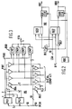
- the cache includes a store STR 40 which stores data words.
- This store is divided into 4 levels LVO to LV3, and each level contains 1024 storage locations, each of which is 20 bits long.
- 20-bit data words are fed into the store, and read from it, over a 20 bit wide data bus DTA.
- Each of the 4 levels of the store is addressed by the 10-bit LSA portion of the main memory address of the data word.
- each of the 4 levels has an enable input, which has to be enabled for the level to be enabled.
- the enable inputs are respective bits from a 4-bit chip enable bus CHS.
- each of the 4 levels has a write enable input; the state of this input determines whether the level is read from or written in.
- the write enable inputs are respective bits from a 4-bit write enable bus WRS.
- a directory section DIR 84 stores the MSA address portions of the addresses of the words stored in the store 40.
- the LSA portion addresses four locations, one in each of the four levels LVO to LV3, of the store 40, and this same LSA address portion addresses the corresponding four locations, one in each of the four levels LVO to LV3 into which the directory 84 is divided, in the directory.
- the four stored MSA address portions (of the four words in the store 40) are thereby read out and fed to a comparator unit COMP 421, which is also divided into four levels LVO to LV3.
- the four levels of the comparator 421 are also fed with the MSA portion of the address of the desired word.
- Each of the four levels of the comparator unit produces a "hit" signal if there is a match between the two MSA address portions fed to it, and the four outputs together form a 4-bit hit bus HIT.
- These hit signals are combined with write control signals on a 4-bit bus WRC in a selector unit 430, to produce the chip enable signals on bus CHS to the store 40.
- WRC write control signals
- a selector unit 430 to produce the chip enable signals on bus CHS to the store 40.
- the desired word is not already resident in the cache. That will be indicated by all four of the outputs of the comparator unit 421 indicating a miss. If this happens, an existing word in the cache must be displaced and the new word written in.
- the selection of the level into which the new word is written is determined in accordance with a "round robin" algorithm, which selects the four levels 0, 1, 2, 3, 0, etc cyclically for successive new words. This is controlled by a round robin counter unit RR 80, which is coupled to the write control unit W CTL 82 which generates the write select signals WRS. It is also coupled to a mode control unit M CTL 86, which controls the writing of the MSA portion of the address of the new word in the directory 84.
- FIG. 2 shows the round robin unit 80.
- the 2-bit number for the appropriate column is therefore read out, and is stored in a pair of flip-flops RDO, RD1.
- This number indicates the level in which the next word is to be written, and the two outputs RDO, RD1 are fed to the write control unit 82 for decoding to generate the 1-out-of-4 signal WRS, which is fed to the store 40 and the directory 84 to select the appropriate level for writing. If a fresh word is being written, the round robin count for that level must also be updated, i.e.
- a round robin clear flip-flop RDC is controlled, by suitable timing signals not shown, to clear the two flip- flops RDO and RD1 appropriately and control them for such matters as initialization.
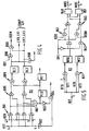
- Figure 3 shows part of the mode control circuit 86. Since the four output address portions from the four levels of the directory 84 are different, and all four are fed individually to the comparator unit 421, the MSA address portion must be buffered separately to each level. This is done by the four sets of buffers 863. In addition, the MSA portion is divided into two 5-bit sections, which are fed to two respective parity generators PG1, PG2, each of which generates a parity bit and its complement. The two parity bits are combined on a 2-bit even parity bus PBE, and are buffered through four sets of buffers 864 to the four levels of the directory 84, so that the buses to the directory are 12 bits, 10 for the MSA portion plus 2 for parity.
- each level of the directory 84 when a desired address is being searched for in the cache, is thus a 12-bit signal, 10 bits MSA portion plus 2 bits parity.
- the 10-bit MSA portion is fed to the corresponding level of the comparator unit 421, for comparison with the MSA portion of the desired address.
- the 2 parity bits are fed back to the circuitry shown in Figure 3, and passed to a corresponding one of four parity comparators 860.
- the MSA portion of the desired address is fed to the parity generators PG1, PG2, to generate a 2-bit odd parity signal PBO, which is also fed to the four comparators 860 (each of which may comprise a pair of Exclusive-OR gates feeding a NOR gate). These generate a 4-bit hit enable signal HEN.
- the use of both even and odd parity bits, one for storage in the directory and the other for comparison with the stored bit results in a simplification and saving in logic levels.
- the hit enable signals HEN are combined with the hit signals HIT in a further portion of the mode control circuit 86, shown in Figure 4.
- the hit enable signals are the result of comparing parity bits generated from the desired MSA address portion with the parity bits of the stored MSA address portions, and obviously it is only in the event of a hit that this comparison is meaningful.
- the hit enable signals HEN are combined with the corresponding hit signals HIT, by a set of four gates 881. Negative logic is in fact used at this point, so that the outputs of these gates will normally be 1.
- a hit will give one 0 input to one of these gates, and the hit enable signal for that gate should also be 0 (representing a match between the parity bits of the stored MSA address portion for that level and the desired MSA address portion, these being identical since there was a hit).
- the presence of all ones or otherwise of a 0 from one of the gates 881 is detected by a gate 887, which sets a first parity error flip-flop PEO accordingly. This in turn sets a second parity error flip-flop PE1.
- a gate 902 which is fed with all bits of the HIT bus.
- This gate feeds a gate 904, which is also fed from the gate 887 via an inverter 903.
- the output of gate 904 indicates when there has been a valid hit - i.e. a hit which was not accompanied by a parity error.
- the output of this gate is used to determine whether or not a fresh word is to be written into the cache.
- an error in the directory 84 may change either a bit of the MSA portion or a parity bit.
- the hit will actually be valid, but cannot be relied on since the parity is wrong.
- a hit may occur which is truly invalid, since the theoretical true stored MSA portion does not match the desired MSA portion.
- the parity comparison will fail, since the stored parity bits will be those for the true stored MSA portion, not what the stored MSA portion has become as a result of the error, and will not match the parity bits for the desired MSA portion.
- the outputs of the four gates 881 are combined by two gates 885, to determine whether the error occurred in the pair of levels 0 and 1, or in the pair of levels 2 and 3. These two gates feed two respective degrade level flip-flops DL1 and DL2 via a pair of gates 889, which are enabled by the setting of the first parity error flip-flop PEO.
- a parity error in level 0 or 1 sets flip-flop DL1; a parity error in level 2 or 3 sets flip-flop DL2.
- the cache can still operate though in a degraded mode if either one of the flip-flops DL1 and DL2 is set. If both are set, however, the cache cannot operate at all. This state is detected and signalled to the CPU by a gate 898.
- the setting of a degrade level flip-flop indicates that the corresponding pair of levels are not reliable, and must therefore no longer be used. Accordingly, the two signals DL1 and DL2 from these two flip-flops are fed to the four comparators of the comparator unit 421, as shown in Figure 1. Signal DL1 is fed to levels 0 and 1, so as to disable the comparisons for these two levels when flip-flop DL1 is set; similarly, signal DL2 is used to disable the comparisons for levels 2 and 3 when an error has occurred in either of these two levels.
- Figure 5 shows the write control circuitry 82 in detail. This has to select the appropriate level for writing in two situations; writing after a hit, and writing a new word if there has been no hit.
- the level in which the hit occurred is coded by means of a pair of write select flip-flops WSO and WS1. As shown, these two flip-flops are fed from the HIT bus by means of two gates 821, which are fed with the level 0, 1, and 2 HIT signals HTO, HT1, and HT2 as shown. Thus flip-flop WSO is set if there is a hit in levels 0 or 1, and flip-flop WS1 is set if there is a hit in levels 2 or 3. (The HIT bus uses negative logic.)
- a signal RPL determines whether the write selection is for replacement (no hit) or simple rewriting of a word already in the cache (a hit). For rewriting, the complement of signal RPL enables a pair of gates 843 to pass the outputs of the two flip-flops WSO and WS1. For replacement, signal RPL enables a pair of gates 841, which are fed with the signals RDO and RDM, derived respectively from the two round robin flip-flops RDO and RD1. The selected pair of signals pass through a further pair of gates 845 to a pair of decoders 848 and 851, which decode the 2-bit signals from gates 845 into the 1-out-of-4 signals of buses WRS and WRC. Two separate decoders are used because this allows separate enable control of the two buses WRS and WRC. It is necessary to be able to enable these two buses separately because bus WRC is used, via the selector unit 430, for reading as well as writing in the store 40.
- the flip-flop RD1 selects between the two lower levels 0 and 1 and the two upper levels 2 and 3, while the flip-flop RDO selects between level 0 and level 1, or between level 2 and level 3.
- the two gates 896 and 895 determine signal RDM in dependence on signal RD1 such that if neither of the degrade level flip-flops DL1 and DL2 is set (normal operation), signal RDM is the same as RD1; if flip-flop DL1 is set, indicating an error in levels 0 and 1, signal RDM is forced to 1; while if flip-flop DL2 is set, indicating an error in levels 2 and 3, signal RDM is forced to 0.
- the level for replacement will normally be selected in cyclic sequence, but if an error has occurred in levels 0 or 1, only levels 2 and 3 can be selected (cyclically) for replacement, while if an error has occurred in levels 2 and 3, only levels 0 and 1 can be selected (cyclically) for replacement.
- the level selection between the two available levels for replacement in the event of a failure in the other two levels is still determined for each column (LSA portion) independently by the round robin unit 80.
Landscapes
- Engineering & Computer Science (AREA)
- Theoretical Computer Science (AREA)
- Physics & Mathematics (AREA)
- General Engineering & Computer Science (AREA)
- General Physics & Mathematics (AREA)
- Memory System Of A Hierarchy Structure (AREA)
- Techniques For Improving Reliability Of Storages (AREA)
Claims (9)
caractérisée par le fait que les moyens de remplacement (80) comprennent des moyens de comptage à exécution circulaire et des moyens de bascule de niveau (RDO, RD1) pour enregistrer des informations codées qui désignent, pour chaque colonne, un niveau suivant parmi lesdits niveaux, dans lequel la donnée de remplacement doit être écrite;
Applications Claiming Priority (2)
| Application Number | Priority Date | Filing Date | Title |
|---|---|---|---|
| US364052 | 1982-03-31 | ||
| US06/364,052 US4464717A (en) | 1982-03-31 | 1982-03-31 | Multilevel cache system with graceful degradation capability |
Publications (3)
| Publication Number | Publication Date |
|---|---|
| EP0090638A2 EP0090638A2 (fr) | 1983-10-05 |
| EP0090638A3 EP0090638A3 (en) | 1987-04-08 |
| EP0090638B1 true EP0090638B1 (fr) | 1991-01-16 |
Family
ID=23432812
Family Applications (1)
| Application Number | Title | Priority Date | Filing Date |
|---|---|---|---|
| EP83301749A Expired EP0090638B1 (fr) | 1982-03-31 | 1983-03-29 | Système à mémoire-antémémoire |
Country Status (9)
| Country | Link |
|---|---|
| US (1) | US4464717A (fr) |
| EP (1) | EP0090638B1 (fr) |
| JP (1) | JPS58179982A (fr) |
| AU (1) | AU549615B2 (fr) |
| BR (1) | BR8301593A (fr) |
| CA (1) | CA1184665A (fr) |
| DE (1) | DE3382111D1 (fr) |
| FI (1) | FI80352C (fr) |
| MX (1) | MX154471A (fr) |
Families Citing this family (52)
| Publication number | Priority date | Publication date | Assignee | Title |
|---|---|---|---|---|
| US4686621A (en) * | 1983-06-30 | 1987-08-11 | Honeywell Information Systems Inc. | Test apparatus for testing a multilevel cache system with graceful degradation capability |
| US4667288A (en) * | 1983-06-30 | 1987-05-19 | Honeywell Information Systems Inc. | Enable/disable control checking apparatus |
| US4646237A (en) * | 1983-12-05 | 1987-02-24 | Ncr Corporation | Data handling system for handling data transfers between a cache memory and a main memory |
| US4740889A (en) * | 1984-06-26 | 1988-04-26 | Motorola, Inc. | Cache disable for a data processor |
| CA1233271A (fr) * | 1984-06-26 | 1988-02-23 | David S. Mothersole | Circuit d'invalidation d'antememoire pour processeur de donnees |
| US4823259A (en) * | 1984-06-29 | 1989-04-18 | International Business Machines Corporation | High speed buffer store arrangement for quick wide transfer of data |
| US4737909A (en) * | 1985-04-01 | 1988-04-12 | National Semiconductor Corp. | Cache memory address apparatus |
| US4755930A (en) * | 1985-06-27 | 1988-07-05 | Encore Computer Corporation | Hierarchical cache memory system and method |
| JPS62194563A (ja) * | 1986-02-21 | 1987-08-27 | Hitachi Ltd | バツフア記憶装置 |
| US5237671A (en) * | 1986-05-02 | 1993-08-17 | Silicon Graphics, Inc. | Translation lookaside buffer shutdown scheme |
| US4802087A (en) * | 1986-06-27 | 1989-01-31 | Honeywell Bull Inc. | Multiprocessor level change synchronization apparatus |
| JPS6324428A (ja) * | 1986-07-17 | 1988-02-01 | Mitsubishi Electric Corp | キヤツシユメモリ |
| AU604101B2 (en) * | 1987-04-13 | 1990-12-06 | Computervision Corporation | High availability cache organization |
| US4833601A (en) * | 1987-05-28 | 1989-05-23 | Bull Hn Information Systems Inc. | Cache resiliency in processing a variety of address faults |
| US5136691A (en) * | 1988-01-20 | 1992-08-04 | Advanced Micro Devices, Inc. | Methods and apparatus for caching interlock variables in an integrated cache memory |
| ATE109910T1 (de) * | 1988-01-20 | 1994-08-15 | Advanced Micro Devices Inc | Organisation eines integrierten cachespeichers zur flexiblen anwendung zur unterstützung von multiprozessor-operationen. |
| US5025366A (en) * | 1988-01-20 | 1991-06-18 | Advanced Micro Devices, Inc. | Organization of an integrated cache unit for flexible usage in cache system design |
| US4912630A (en) * | 1988-07-29 | 1990-03-27 | Ncr Corporation | Cache address comparator with sram having burst addressing control |
| US5067078A (en) * | 1989-04-17 | 1991-11-19 | Motorola, Inc. | Cache which provides status information |
| US5070502A (en) * | 1989-06-23 | 1991-12-03 | Digital Equipment Corporation | Defect tolerant set associative cache |
| JPH0359741A (ja) * | 1989-07-28 | 1991-03-14 | Mitsubishi Electric Corp | キャッシュメモリ |
| US5317718A (en) * | 1990-03-27 | 1994-05-31 | Digital Equipment Corporation | Data processing system and method with prefetch buffers |
| US5347648A (en) * | 1990-06-29 | 1994-09-13 | Digital Equipment Corporation | Ensuring write ordering under writeback cache error conditions |
| US5155843A (en) * | 1990-06-29 | 1992-10-13 | Digital Equipment Corporation | Error transition mode for multi-processor system |
| US5454093A (en) * | 1991-02-25 | 1995-09-26 | International Business Machines Corporation | Buffer bypass for quick data access |
| US5280591A (en) * | 1991-07-22 | 1994-01-18 | International Business Machines, Corporation | Centralized backplane bus arbiter for multiprocessor systems |
| US5345576A (en) * | 1991-12-31 | 1994-09-06 | Intel Corporation | Microprocessor simultaneously issues an access to an external cache over an external cache bus and to an internal cache, cancels the external cache access on an internal cache hit, and reissues the access over a main memory bus on an external cache miss |
| US5649154A (en) * | 1992-02-27 | 1997-07-15 | Hewlett-Packard Company | Cache memory system having secondary cache integrated with primary cache for use with VLSI circuits |
| US5530823A (en) * | 1992-05-12 | 1996-06-25 | Unisys Corporation | Hit enhancement circuit for page-table-look-aside-buffer |
| US5905997A (en) * | 1994-04-29 | 1999-05-18 | Amd Inc. | Set-associative cache memory utilizing a single bank of physical memory |
| US5826052A (en) * | 1994-04-29 | 1998-10-20 | Advanced Micro Devices, Inc. | Method and apparatus for concurrent access to multiple physical caches |
| US5768295A (en) * | 1995-03-10 | 1998-06-16 | Nec Corporation | System for parity calculation based on arithemtic difference between data |
| JP2799983B2 (ja) * | 1996-02-16 | 1998-09-21 | 三信工業株式会社 | 船舶推進機のエンジン冷却装置 |
| US5875201A (en) * | 1996-12-30 | 1999-02-23 | Unisys Corporation | Second level cache having instruction cache parity error control |
| US5894487A (en) * | 1997-07-15 | 1999-04-13 | International Business Machines Corporation | Error detection of directory arrays in dynamic circuits |
| US6049845A (en) * | 1997-11-05 | 2000-04-11 | Unisys Corporation | System and method for providing speculative arbitration for transferring data |
| US6014709A (en) * | 1997-11-05 | 2000-01-11 | Unisys Corporation | Message flow protocol for avoiding deadlocks |
| US6052760A (en) * | 1997-11-05 | 2000-04-18 | Unisys Corporation | Computer system including plural caches and utilizing access history or patterns to determine data ownership for efficient handling of software locks |
| US6092156A (en) * | 1997-11-05 | 2000-07-18 | Unisys Corporation | System and method for avoiding deadlocks utilizing split lock operations to provide exclusive access to memory during non-atomic operations |
| AT406461B (de) * | 1997-12-15 | 2000-05-25 | Fronius Schweissmasch | Schweissbrenner |
| US6314501B1 (en) | 1998-07-23 | 2001-11-06 | Unisys Corporation | Computer system and method for operating multiple operating systems in different partitions of the computer system and for allowing the different partitions to communicate with one another through shared memory |
| US6687818B1 (en) | 1999-07-28 | 2004-02-03 | Unisys Corporation | Method and apparatus for initiating execution of an application processor in a clustered multiprocessor system |
| US6665761B1 (en) | 1999-07-28 | 2003-12-16 | Unisys Corporation | Method and apparatus for routing interrupts in a clustered multiprocessor system |
| JP3812258B2 (ja) * | 2000-01-13 | 2006-08-23 | 株式会社日立製作所 | キャッシュ記憶装置 |
| US6728823B1 (en) * | 2000-02-18 | 2004-04-27 | Hewlett-Packard Development Company, L.P. | Cache connection with bypassing feature |
| US6918071B2 (en) * | 2001-04-20 | 2005-07-12 | Sun Microsystems, Inc. | Yield improvement through probe-based cache size reduction |
| US7099318B2 (en) * | 2001-12-28 | 2006-08-29 | Intel Corporation | Communicating message request transaction types between agents in a computer system using multiple message groups |
| US7191375B2 (en) * | 2001-12-28 | 2007-03-13 | Intel Corporation | Method and apparatus for signaling an error condition to an agent not expecting a completion |
| US7184399B2 (en) * | 2001-12-28 | 2007-02-27 | Intel Corporation | Method for handling completion packets with a non-successful completion status |
| US7581026B2 (en) * | 2001-12-28 | 2009-08-25 | Intel Corporation | Communicating transaction types between agents in a computer system using packet headers including format and type fields |
| US7472038B2 (en) * | 2007-04-16 | 2008-12-30 | International Business Machines Corporation | Method of predicting microprocessor lifetime reliability using architecture-level structure-aware techniques |
| GB2505179A (en) * | 2012-08-20 | 2014-02-26 | Ibm | Managing a data cache for a computer system |
Family Cites Families (15)
| Publication number | Priority date | Publication date | Assignee | Title |
|---|---|---|---|---|
| US932005A (en) * | 1903-07-31 | 1909-08-24 | United Shoe Machinery Ab | Machine for making lacing-hooks. |
| US3685020A (en) * | 1970-05-25 | 1972-08-15 | Cogar Corp | Compound and multilevel memories |
| US3820078A (en) * | 1972-10-05 | 1974-06-25 | Honeywell Inf Systems | Multi-level storage system having a buffer store with variable mapping modes |
| US3848234A (en) * | 1973-04-04 | 1974-11-12 | Sperry Rand Corp | Multi-processor system with multiple cache memories |
| US4020466A (en) * | 1974-07-05 | 1977-04-26 | Ibm Corporation | Memory hierarchy system with journaling and copy back |
| JPS5721799B2 (fr) * | 1975-02-01 | 1982-05-10 | ||
| US4053752A (en) * | 1975-09-15 | 1977-10-11 | International Business Machines Corporation | Error recovery and control in a mass storage system |
| FR2361718A1 (fr) * | 1976-08-11 | 1978-03-10 | Adersa | Processeur parallele associatif a hierarchie de memoire, notamment pour l'acquisition et le traitement rapides des signaux |
| US4084236A (en) * | 1977-02-18 | 1978-04-11 | Honeywell Information Systems Inc. | Error detection and correction capability for a memory system |
| US4195343A (en) * | 1977-12-22 | 1980-03-25 | Honeywell Information Systems Inc. | Round robin replacement for a cache store |
| US4195342A (en) * | 1977-12-22 | 1980-03-25 | Honeywell Information Systems Inc. | Multi-configurable cache store system |
| JPS5542318A (en) * | 1978-09-14 | 1980-03-25 | Nec Corp | Cash memory control system |
| US4168541A (en) * | 1978-09-25 | 1979-09-18 | Sperry Rand Corporation | Paired least recently used block replacement system |
| JPS5687280A (en) * | 1979-12-14 | 1981-07-15 | Hitachi Ltd | Data processor |
| US4342084A (en) * | 1980-08-11 | 1982-07-27 | International Business Machines Corporation | Main storage validation means |
-
1982
- 1982-03-31 US US06/364,052 patent/US4464717A/en not_active Expired - Fee Related
-
1983
- 1983-02-25 AU AU11855/83A patent/AU549615B2/en not_active Ceased
- 1983-03-02 CA CA000422724A patent/CA1184665A/fr not_active Expired
- 1983-03-18 MX MX196626A patent/MX154471A/es unknown
- 1983-03-28 BR BR8301593A patent/BR8301593A/pt unknown
- 1983-03-29 DE DE8383301749T patent/DE3382111D1/de not_active Expired - Fee Related
- 1983-03-29 EP EP83301749A patent/EP0090638B1/fr not_active Expired
- 1983-03-30 FI FI831080A patent/FI80352C/fi not_active IP Right Cessation
- 1983-03-31 JP JP58054086A patent/JPS58179982A/ja active Pending
Also Published As
| Publication number | Publication date |
|---|---|
| JPS58179982A (ja) | 1983-10-21 |
| FI80352C (fi) | 1990-05-10 |
| US4464717A (en) | 1984-08-07 |
| FI80352B (fi) | 1990-01-31 |
| EP0090638A3 (en) | 1987-04-08 |
| EP0090638A2 (fr) | 1983-10-05 |
| BR8301593A (pt) | 1983-12-06 |
| MX154471A (es) | 1987-08-28 |
| CA1184665A (fr) | 1985-03-26 |
| AU549615B2 (en) | 1986-02-06 |
| FI831080L (fi) | 1983-10-01 |
| DE3382111D1 (de) | 1991-02-21 |
| AU1185583A (en) | 1983-10-06 |
| FI831080A0 (fi) | 1983-03-30 |
Similar Documents
| Publication | Publication Date | Title |
|---|---|---|
| EP0090638B1 (fr) | Système à mémoire-antémémoire | |
| US5267242A (en) | Method and apparatus for substituting spare memory chip for malfunctioning memory chip with scrubbing | |
| US4945512A (en) | High-speed partitioned set associative cache memory | |
| US4357656A (en) | Method and apparatus for disabling and diagnosing cache memory storage locations | |
| US4168541A (en) | Paired least recently used block replacement system | |
| US3668644A (en) | Failsafe memory system | |
| US4833601A (en) | Cache resiliency in processing a variety of address faults | |
| US4375664A (en) | Apparatus for detecting, correcting and logging single bit memory read errors using syndrome generating and decoding circuitry | |
| US4051461A (en) | Management table apparatus in memory hierarchy system | |
| US5313475A (en) | ECC function with self-contained high performance partial write or read/modify/write and parity look-ahead interface scheme | |
| US5142540A (en) | Multipart memory apparatus with error detection | |
| US4506364A (en) | Memory address permutation apparatus | |
| US4483003A (en) | Fast parity checking in cache tag memory | |
| US3436734A (en) | Error correcting and repairable data processing storage system | |
| CA1151305A (fr) | Circuit de detection d'erreurs dans les enregistrements en memoire | |
| US6987684B1 (en) | Content addressable memory (CAM) devices having multi-block error detection logic and entry selective error correction logic therein | |
| EP0259967B1 (fr) | Mémoire répertoire | |
| EP0689695B1 (fr) | Systeme de memoire insensible aux defaillances | |
| EP0186719A1 (fr) | Dispositif pour la correction d'erreurs dans des mémoires | |
| US3576982A (en) | Error tolerant read-only storage system | |
| JPH04277848A (ja) | メモリフォルトマッピング装置、検出エラーのマッピング方法及びマルチパスメモリフォルトマッピング装置 | |
| US4926426A (en) | Error correction check during write cycles | |
| EP0090219B1 (fr) | Système de mémoire restructuré par algorithme de permutation déterministe | |
| JPS6310460B2 (fr) | ||
| EP0279396B1 (fr) | Antémémoire comportant l'autovérification d'erreur et des circuits de vérification séquentiels |
Legal Events
| Date | Code | Title | Description |
|---|---|---|---|
| PUAI | Public reference made under article 153(3) epc to a published international application that has entered the european phase |
Free format text: ORIGINAL CODE: 0009012 |
|
| AK | Designated contracting states |
Kind code of ref document: A2 Designated state(s): BE CH DE FR GB IT LI NL SE |
|
| PUAL | Search report despatched |
Free format text: ORIGINAL CODE: 0009013 |
|
| AK | Designated contracting states |
Kind code of ref document: A3 Designated state(s): BE CH DE FR GB IT LI NL SE |
|
| RAP1 | Party data changed (applicant data changed or rights of an application transferred) |
Owner name: HONEYWELL BULL INC. |
|
| 17P | Request for examination filed |
Effective date: 19871008 |
|
| 17Q | First examination report despatched |
Effective date: 19880511 |
|
| RAP1 | Party data changed (applicant data changed or rights of an application transferred) |
Owner name: BULL HN INFORMATION SYSTEMS INC. |
|
| ITF | It: translation for a ep patent filed |
Owner name: BARZANO' E ZANARDO ROMA S.P.A. |
|
| GRAA | (expected) grant |
Free format text: ORIGINAL CODE: 0009210 |
|
| AK | Designated contracting states |
Kind code of ref document: B1 Designated state(s): BE CH DE FR GB IT LI NL SE |
|
| PG25 | Lapsed in a contracting state [announced via postgrant information from national office to epo] |
Ref country code: NL Effective date: 19910116 Ref country code: FR Effective date: 19910116 Ref country code: BE Effective date: 19910116 |
|
| REF | Corresponds to: |
Ref document number: 3382111 Country of ref document: DE Date of ref document: 19910221 |
|
| PG25 | Lapsed in a contracting state [announced via postgrant information from national office to epo] |
Ref country code: SE Effective date: 19910330 |
|
| PG25 | Lapsed in a contracting state [announced via postgrant information from national office to epo] |
Ref country code: LI Effective date: 19910331 Ref country code: CH Effective date: 19910331 |
|
| PG25 | Lapsed in a contracting state [announced via postgrant information from national office to epo] |
Ref country code: GB Effective date: 19910416 |
|
| EN | Fr: translation not filed | ||
| NLV1 | Nl: lapsed or annulled due to failure to fulfill the requirements of art. 29p and 29m of the patents act | ||
| PLBE | No opposition filed within time limit |
Free format text: ORIGINAL CODE: 0009261 |
|
| STAA | Information on the status of an ep patent application or granted ep patent |
Free format text: STATUS: NO OPPOSITION FILED WITHIN TIME LIMIT |
|
| REG | Reference to a national code |
Ref country code: CH Ref legal event code: PL |
|
| GBPC | Gb: european patent ceased through non-payment of renewal fee | ||
| PG25 | Lapsed in a contracting state [announced via postgrant information from national office to epo] |
Ref country code: DE Effective date: 19920101 |
|
| 26N | No opposition filed | ||
| EUG | Se: european patent has lapsed |
Ref document number: 83301749.4 Effective date: 19911009 |