EP0088134A1 - Solid state image pickup device - Google Patents
Solid state image pickup device Download PDFInfo
- Publication number
- EP0088134A1 EP0088134A1 EP82902747A EP82902747A EP0088134A1 EP 0088134 A1 EP0088134 A1 EP 0088134A1 EP 82902747 A EP82902747 A EP 82902747A EP 82902747 A EP82902747 A EP 82902747A EP 0088134 A1 EP0088134 A1 EP 0088134A1
- Authority
- EP
- European Patent Office
- Prior art keywords
- transfer
- image pickup
- vertical transfer
- horizontal
- vertical
- Prior art date
- Legal status (The legal status is an assumption and is not a legal conclusion. Google has not performed a legal analysis and makes no representation as to the accuracy of the status listed.)
- Granted
Links
- 239000007787 solid Substances 0.000 title claims abstract description 56
- 238000003860 storage Methods 0.000 claims abstract description 27
- 238000001444 catalytic combustion detection Methods 0.000 description 8
- 230000007547 defect Effects 0.000 description 7
- 238000010586 diagram Methods 0.000 description 4
- 230000002950 deficient Effects 0.000 description 3
- 238000005036 potential barrier Methods 0.000 description 3
- 239000004065 semiconductor Substances 0.000 description 3
- 239000000758 substrate Substances 0.000 description 3
- 239000012535 impurity Substances 0.000 description 2
- 238000000034 method Methods 0.000 description 2
- 206010027146 Melanoderma Diseases 0.000 description 1
- 241000519995 Stachys sylvatica Species 0.000 description 1
- 230000002730 additional effect Effects 0.000 description 1
- 230000005669 field effect Effects 0.000 description 1
- 238000005468 ion implantation Methods 0.000 description 1
- 238000004519 manufacturing process Methods 0.000 description 1
- 230000007847 structural defect Effects 0.000 description 1
Images


Classifications
-
- H—ELECTRICITY
- H04—ELECTRIC COMMUNICATION TECHNIQUE
- H04N—PICTORIAL COMMUNICATION, e.g. TELEVISION
- H04N3/00—Scanning details of television systems; Combination thereof with generation of supply voltages
- H04N3/10—Scanning details of television systems; Combination thereof with generation of supply voltages by means not exclusively optical-mechanical
- H04N3/14—Scanning details of television systems; Combination thereof with generation of supply voltages by means not exclusively optical-mechanical by means of electrically scanned solid-state devices
- H04N3/15—Scanning details of television systems; Combination thereof with generation of supply voltages by means not exclusively optical-mechanical by means of electrically scanned solid-state devices for picture signal generation
-
- H—ELECTRICITY
- H01—ELECTRIC ELEMENTS
- H01L—SEMICONDUCTOR DEVICES NOT COVERED BY CLASS H10
- H01L27/00—Devices consisting of a plurality of semiconductor or other solid-state components formed in or on a common substrate
- H01L27/14—Devices consisting of a plurality of semiconductor or other solid-state components formed in or on a common substrate including semiconductor components sensitive to infrared radiation, light, electromagnetic radiation of shorter wavelength or corpuscular radiation and specially adapted either for the conversion of the energy of such radiation into electrical energy or for the control of electrical energy by such radiation
- H01L27/144—Devices controlled by radiation
- H01L27/146—Imager structures
- H01L27/148—Charge coupled imagers
- H01L27/14831—Area CCD imagers
-
- H—ELECTRICITY
- H04—ELECTRIC COMMUNICATION TECHNIQUE
- H04N—PICTORIAL COMMUNICATION, e.g. TELEVISION
- H04N25/00—Circuitry of solid-state image sensors [SSIS]; Control thereof
- H04N25/70—SSIS architectures; Circuits associated therewith
- H04N25/71—Charge-coupled device [CCD] sensors; Charge-transfer registers specially adapted for CCD sensors
- H04N25/713—Transfer or readout registers; Split readout registers or multiple readout registers
-
- H—ELECTRICITY
- H04—ELECTRIC COMMUNICATION TECHNIQUE
- H04N—PICTORIAL COMMUNICATION, e.g. TELEVISION
- H04N25/00—Circuitry of solid-state image sensors [SSIS]; Control thereof
- H04N25/70—SSIS architectures; Circuits associated therewith
- H04N25/71—Charge-coupled device [CCD] sensors; Charge-transfer registers specially adapted for CCD sensors
- H04N25/73—Charge-coupled device [CCD] sensors; Charge-transfer registers specially adapted for CCD sensors using interline transfer [IT]
Definitions
- This invention relates to solid state image pickup apparatus employing a solid state image pickup device which comprises a charge transfer device, and more particularly, is directed to an improved solid state image pickup apparatus employing a solid state image pickup device of the interline transfer type, in which the driving condition for charge transfer performed in the solid state image pickup device is contrived so that a certain defect on a reproduced picture obtained in response to an image pickup signal output derived therefrom is eliminated.
- Solid state image pickup devices comprising a charge transfer device such as a charge coupled device ( hereinafter referred to as a CCD ) are classified broadly into the frame transfer type and the interline transfer type, and each of them is utilized in different way so as to make a good use of its advantages and features.
- a charge transfer device such as a charge coupled device ( hereinafter referred to as a CCD )
- CCD charge coupled device
- One example of the solid state image pickup device of the interline transfer type using the CCD comprises a photo-sensing and vertical transfer portion which includes a plurality of photodetectors arranged in horizontal and vertical rows and vertical transfer portions each formed with a group of CCDs and extending along each of the vertical rows of the photodetectors, a horizontal transfer portion coupled with the photo-sensing and vertical transfer portion and an output portion coupled with the horizontal transfer portion and provided with an signal output terminal, the whole of which are formed on a common semiconductor substrate.
- a vertical driving signal for vertical charge transfer is applied to the vertical transfer portions through vertical transfer electrodes which are provided on an insulating layer overspreading the photo-sensing and vertical transfer portion and a horizontal driving signal for horizontal charge transfer is applied to the horizontal transfer portion through horizontal transfer electrodes which are provided on an insulating layer overspreading the horizontal transfer portion, so that vertical charge transfer operation and horizontal charge transfer operation are performed.in the vertical transfer portions and the horizontal transfer portion, respectively.
- signal charges obtained in the photodetectors in response to the light received thereby during one frame period are read out to the vertical transfer portions, and then transferred toward the horizontal transfer portion by the vertical charge transfer operation performed in the vertical transfer portion so that the signal charges produced in each horizontal row of the photodetectors are transferred in turn to the horizontal transfer portion.
- the signal charges transferred to the horizontal transfer portion are further transferred to the output portion by the horizontal charge transfer operation performed in the horizontal transfer portion and as a result of this an image pickup signal output is obtained at the signal output terminal.
- This local area of deep potential in the vertical transfer portion appears at a region having high impurity density which is provided undesirably due to nonuniformity in impurity density in the vertical transfer portion or at a region positioned under a thick portion of the insulating layer which is provided undesirably due to nonumiformity in thickness of the insulating layer on the vertical transfer portion, and is a structural defect in the image pickup device.
- an insulated gate field effect transistor ( hereinafter referred to as a MOS FET ) having its source at the local area of deep potential is substantially formed in the vertical transfer portion and a flow of charges is caused from the local area of deep potential to an advanced potential well in the vertical transfer portion as a sub-threshold current of the MOS FET. If a charge transfer period in which each charge transfer in the vertical transfer portions is carried out is constant and the manner of repetition of such charge transfer periods is made uniform, the amount of charges flowing into the advanced potential well from the local area of deep potential is not varied and therefore the charges flowing into the advanced potential well from the local area of deep potential do not raise any serious problem.
- a charge transfer period in which each charge transfer in the vertical transfer portions is carried out is constant and the manner of repetition of such charge transfer periods is made uniform, the amount of charges flowing into the advanced potential well from the local area of deep potential is not varied and therefore the charges flowing into the advanced potential well from the local area of deep potential do not raise any serious problem.
- an object of the present invention to provide an solid state image pickup apparatus employing a solid state image pickup device of the interline transfer type, in which the driving condition for charge transfer performed in vertical transfer portions provided in the solid state image pickup device is improved so that a charge transfer period in which each charge transfer in the vertical transfer portions is carried out is made uniform and consequently an image pickup signal output from which a picture without the defect called usually " white and black spots " is reproduced can be obtained from the apparatus.
- a solid state image pickup apparatus employing a solid state image pickup device of the interline transfer type which comprises a plurality of photodetectors arranged vertically and horizontally, transfer gate areas each corresponding to each of the photodetectors, vertical transfer portions, a horizontal transfer portion and an output portion; a reading pulse voltage taking a first high level is applied to each of two transfer gata areas adjacent in the vertical direction alternately at every field period, a voltage taking a second high level lower than the first high level is applied to the storage regions of the vertical transfer portions during each horizontal video period, and transfer pulse voltages taking a low level in turn at the respective different phases within each horizontal blanking period are applied to the vertical transfer portions.
- signal charges are read out to the storage regions of the vertical transfer portions from the photodetectors corresponding to the transfer gate areas to which the reading pulse voltage taking the first high level is applied, then transferred vertically through the vertical transfer portions to the horizontal transfer portion in response to the transfer pulse voltages applied to the vertical transfer portions in the horizontal blanking period and further transferred horizontally through the horizontal transfer portion to the output portion.
- the solid state image pickup apparatus thus constituted in accordance with the present invention, even if the solid state image pickup device of the interline transfer type employed therein contains a defective local area having deep potential in the vertical transfer portions, an image pickup signal output, which is produced in accordance with the frame interlace reading manner and does not cause a defect on a picture reproduced therefrom which otherwith would be resulted from the defective local area in the image pickup device, can be obtained. Futher, since the image pickup device containing therein such a defective local area can be use as a normal device, the yield rate in manufacturing is substantially improved.
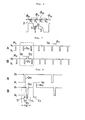
- FIG. 1 An example of a solid state image pickup device of the interline transfer type using a CCD is constituted as shown in Figure 1, and comprises a photo-sensing and vertical transfer portion 3 which includes a plurality of photodetectors 1 arranged in horizontal and vertical rows and vertical transfer portions 2 each formed with a group of CCDs and provided along each of the vertical rows of the photodetectors 1, a horizontal transfer portion 4 coupled with the photo-sensing and vertical transfer portion 3 and an output portion 5 coupled with the horizontal transfer portion 4 and provided with a signal output terminal 5a, the whole of which are formed on a common semiconductor substrate.
- a photo-sensing and vertical transfer portion 3 which includes a plurality of photodetectors 1 arranged in horizontal and vertical rows and vertical transfer portions 2 each formed with a group of CCDs and provided along each of the vertical rows of the photodetectors 1, a horizontal transfer portion 4 coupled with the photo-sensing and vertical transfer portion 3 and an output portion 5 coupled with the horizontal transfer portion 4 and provided with a signal
- a predetermined vertical transfer driving signal and a predetermined horizontal transfer driving signal are applied to the vertical transfer portions 2 and the horizontal transfer portion 4, respectively, so that vertical and horizontal charge transfers are performed in the solid state image pickup device.
- driving signals signal charges obtained in the photodetectors 1 in response to the light received thereby during for example, one frame period are read out to the vertical transfer portions 2 and then transferred vertically toward the horizontal transfer portion 4 by the charge transfer operation of the vertical transfer portions 2 during each horizontal blanking period so that the signal charges produced in each horizontal row of the photodetectors 1 are transferred in turn to the horizontal transfer portion 4.
- the signal charges transferred to the horizontal transfer portion 4 are further transferred horizontally to the output portion 5 by the charge transfer operation of the horizontal transfer portion 4 during each horizontal video period and as a result of this an image pickup signal output is obtained at the signal output terminal 5a.
- the photo-sensing and vertical transfer portion 3 mentioned above contains transfer gate areas 6 provided between each vertical row of the photodetectors 1 and the corresponding one of the vertical transfer portions 2 and a channel stop area 7 provided around each of the photodetectors 1, as shown in Figure 2-A. Further, an overflow drains 8 is provided to be contiguous to each of the channel stop areas 7 and each of the overflow drains 8 and the corresponding one of the vertical transfer portions 2 are separated by a channel stop area 9. On the vertical transfer portions 2, vertical transfer electrodes ⁇ 1 and ⁇ 2 each elongating in the horizontal direction are provided alternately in the vertical direction.
- Each vertical transfer electrode ⁇ 1 is composed of a charge storage electrode ⁇ 1C and a charge transfer electrode ( potential barrier electrode ) ⁇ lt
- each vertical transfer electrode ⁇ 2 is composed of a charge storage electrode ⁇ 2c and a charge transfer electrode ⁇ 2t .
- storage regions are formed under the charge storage electrods ⁇ lc and ⁇ 2C and transfer regions ( potential barrier regions ) are formed under the charge transfer electrodes ⁇ lt and ⁇ 2t , and each transfer region is subjected to the ion implantation or provided thereon with a thick insulating layer so as to have a potential shallower ( lower ) than that of the storage region adjacent thereto and to form a potential barrier.
- FIG. 2-B which shows a sectional view at the position indicated by arrows IIB-IIB in Figure 2-A
- the above mentioned portions and areas. are formed on a semiconductor substrate 10 of, for example, the P type and an insulating layer 11 is provided to cover the whole of these portions and areas thereby with the vertical transfer electrodes ( ⁇ 2 provided thereon.
- the vertical transfer electrodes ⁇ l and ⁇ 2 include transfer gate electrodes at portions thereof, and therefore in Figure 2-B, the vertical transfer electrode ⁇ 2 ( more exactly, the charge storage electrode ⁇ 2c of the vertical transfer electrode ⁇ 2 ) is extended to cover the transfer gate area 6.
- the vertical transfer electrodes ⁇ 1 and ⁇ 2 on the photo-sensing and vertical transfer portion 3 of the solid state image pickup device are supplied with driving signals ⁇ 1 and ⁇ 2 as shown in Figures 3-A and 3-B, respectively, and the voltages of thses driving signals ⁇ l and P2 are applied to the transfer gate areas 6 and the vertical transfer portions 2 positioned under the vertical transfer electrodes ⁇ 1 and ⁇ 2 .
- the driving signals ⁇ 1 and ⁇ 2 With such driving signals ⁇ 1 and ⁇ 2 , the signal charges stored in each two photodetectors 1 adjacent vertically to each other are read out throuth the transfer gate areas 6 to the vertical transfer portions 2 from one of the two photodetectors 1 alternately at every field period so that the signal charges obtained in the photodetectors 1 are read out in the frame interlace reading manner, and the signal charges read out to the vertical transfer portions 2 are transferred vertically to the horizontal transfer portion 4.
- the driving signals ⁇ 1 and ⁇ 2 have reading pulses R 1 and R 2 of high level appearing at every frame period, respectively, and also transfer pulses Q 1 and Q 2 appearing with opposite phases at each horizontal blanking period, respectively. The signal charges are transferred vertically with the high level of the transfer pulse Q1 and the low level of the transfer pulse Q 2.
- the reading pulse R 2 of driving signal ⁇ 2 When the reading pulse R 2 of driving signal ⁇ 2 is supplied to the vertical transfer electrodes ⁇ 2 , the voltage of the reading pulse R 2 is applied to a first group of the transfer gate areas 6 under the vertical transfer electrodes ⁇ 2 and the signal charges stored during one frame period in the photodetectors 1 corresponding to the first group of the transfer gate areas 6 are read out to the vertical transfer portions 2 as signal charges for the first field. Then, the signal charges read out to the vertical transfer portions 2 in response to the reading pulse R 2 are transferred vertically at each horizontal blanking period according to the voltages of the transfer pulses Q 1 and Q 2 applied to the vertical transfer portions 2 under the vertical transfer electrodes ⁇ 1 and ⁇ 2 .
- the reading pulse R 1 of the driving signal ⁇ 1 is supplied to the vertical transfer electrodes ⁇ 1 , the voltage of the reading pulse R 1 is applied to a second group of the transfer gate areas 6 under the vertical transfer electrodes ⁇ 1 and the signal charges stored during one frame period in the photodetectors 1 corresponding to the second group of the transfer gate areas 6 are read out to the vertical transfer portions 2 as signal charges for the second field. Then, the signal charges read out to the vertical transfer portions 2 in response to the reading pulse R l are transferred vertically at each horizontal blanking period according to the voltages of the transfer pulses Q 1 and Q 2 applied to the vertical transfer portions 2 under the vertical transfer electrodes ⁇ 1 and ⁇ 2 . The reading and transferring operation mentioned above is performed repeatedly.
- the signal charges in the photodetectors 1 corresponding to the transfer gate areas 6 which are contiguous to the regions in the vertical transfer portions 2 to which the voltage of the high level of either the driving signal ⁇ 1 ' or ⁇ 2 ' is applied are read out to the vertical transfer portions 2.
- the vertical transfer of the signal charges are carried out in response to the transfer pulses Q 1 and Q 2 in the same manner as taken in the device shown in Figures 2-A and 2-B.
- a MOS FET having its source S made of the area x, its gate G made of the storage region P under the charge storage electrode ⁇ lc and its drain D made of the transfer region P t under the charge transfer electrode ⁇ 2t is substantially formed and a flow of charges arises from the area x under the vertical transfer electrode ⁇ 1 to an advanced potential well in the regions under the vertical transfer electrode ⁇ 2 as a sub-threshold current of the MOS FET. If a charge transfer period in which each charge transfer in the vertical transfer portion 2 is carried out is constant and the interval between such charge transfer periods is made uniform, the amount of charges flowing from the area x to the advanced potential well is not varied and therefore the charges flowing into the advanced potential well do not raise any troublesome problem.
- the charge transfer in the vertical transfer portion 2 is carried out in response to the driving signals ⁇ 1 and ⁇ 2 shown in Figures 3-A and 3-B or the driving signals ⁇ 1 ' and ⁇ 2 ' shown in Figures 5-A and 5-B, and consequently, a long charge transfer period T appears once a frame period, as shown in Figures 3-A and 3-B or the Figures 5-A and 5-B.
- the long charge transfer period T appears to include a reading out period in which the signal charges for the second field are read out to the vertical transfer portion 2.
- the area x transfers the charges stored therein in large quantities compared with the normal amount of charges to the advanced potential well so as to supply excessive signal charges to the latter and, to the contrary, to make the regions positioned behind be lacking in signal charges. This causes the white and black spots in such a manner as aforementioned.
- FIG. 1 One example of a solid state image pickup apparatus according to the present invention is constituted with the solid state image pickup device having the configuration shown in Figures 1, 2-A and 2-B and two-phase driving signals ⁇ 11 and P 12 shown in Figures 7-A and 7-B, which are supplied to the vertical transfer electrodes ⁇ 1 and ⁇ 2 of the solid state image pickup device, respectively.
- the driving signals P 11 and ⁇ 12 are formed into three-level signals, respectively.
- the driving signal ⁇ 11 contains a reading pulse R 11 taking a first high level V R and a transfer pulse Q 11 appearing with the low level V L in each horizontal blanking period and further takes a second high level V H lower than the first high level V R during each horizontal video period.
- the driving signal ⁇ 12 contains a reading pulse R 12 taking the first high level V R and a transfer pulse Q 12 appearing with the low level V L in each horizontal blanking period and further takes the second high level V H during each horizontal video period.
- the transfer pulses Q 11 and Q 12 take the respective phases different from each other in each horizontal blanking period.
- Figure 8 shows in enlarged scale the portions of the driving signals ⁇ 11 and P 12 encircled with a broken line in Figure 7-A and 7-B.
- the transfer pulses Q 11 and Q12 each of which has the pulse width ⁇ 1 of about 2 ⁇ sec, appear with the time difference ⁇ 2 of about 3 ⁇ sec between them within the horizontal blanking period H B, and each of the reading pulses R 11 and R 12 has the pulse width ⁇ 3 of about 20 ⁇ sec.
- the voltage having the second high level V H is applied to the storage regions of the vertical transfer portions 2 under the charge storage electrodes ⁇ 1c and ⁇ 2c and the transfer regions of the vertical transfer portions 2 under the charge transfer electrodes ⁇ 1t and ⁇ 2t during each horizontal video period, and the charge transfer in the vertical transfer portions 2 is carried out when the voltage having the low level V L of the transfer pulse Q 11 is first applied to the regions under the vertical transfer electrodes ⁇ 1 and then the voltage having the low level V L of the transfer pulse Q 12 is applied to the regions under the vertical transfer electrodes ⁇ 2 within each horizontal blanking period.
- the reading pulse R 12 of the driving signal P 12 is supplied to the vertical transfer electrodes ⁇ 2 , the voltage having the first high level V R of the reading pulse R 12 is applied to the transfer gate areas 6 under the charge storage electrodes ⁇ 2c and the signal charges stored during one frame period in the photodetectors 1 corresponding to the transfer gate areas 6 under the charge storage electrodes ⁇ 2c are read out to the storage regions of the vertical transfer portions 2 under the charge storage electrodes ⁇ 2C as signal charges for the first field.
- the reading pulse R 11 of the driving signal ⁇ 11 is supplied to the vertical transfer electrodes ⁇ 1 , the voltage having the first high level V R of the reading pulse R 11 is applied to the transfer gate areas 6 under the charge storage electrodes ⁇ 1C and the signal charges stored during one frame period in the photodetectors 1 corresponding to the transfer gate areas 6 under the charge storage electrodes ⁇ 1c are read out to the storage regions of the vertical transfer portions 2 under the charge storage electrodes ⁇ 1C as signal charges for the second field.
- This reading operation is performed repeatedly and as a result the signal charges obtained in the photodetectors 1 are read out in the frame interlace manner.
- the amplitude V R - V H of each of the reading pulses R 11 and R 12 is selected to be smaller than the amplitude VH - V L of each of the transfer pulses Q 11 and Q 12 , so that the reading pulse R 11 or R 12 is prevented from making such potential steps in the vertical transfer portions 2 as will cause charge transfer in the vertical transfer portions 2.
- a vertical output gate portion at the end of each of the vertical transfer portions 2 and make the vertical output gate portions be in the ON state in response to the transfer pulse Q ll or Q 12 so as to transfer the signal charges to the horizontal transfer portion 4 from the vertical transfer portions 2 in order to prevent the signal charges being in process of transfer in the horizontal transfer portion 4 from flowing into the vertical transfer portions 2.
- the signal charges obtained in the photodetectors 1 are read out to the vertical transfer portions 2 in the frame interlace manner. Further, since the signal charges read out to the vertical transfer portions 2 are transferred in the vertical transfer portions 2 only during the periods of the transfer pulses Q 11 and Q 12 within each horizontal blanking period, the charge transfer period in which each charge transfer in the vertical transfer portions 2 is carried out is kept constant and the interval between such charge transfer periods is made uniform and, as a result of this, an image pickup signal output from which a picture without the white and black spots thereon is reproduced can be obtained at the signal output terminal 5a.
- solid state image pickup device having the vertical transfer portions which are drived to be operative by the two-phase driving signals is employed in the embodiment described above, a solid state image pickup device having vertical transfer portions which are arranged to be drived by a four-phase driving signals can be used for the solid state image pickup apparatus according to the present invention.
- Figure 9 shows the configuration of a photo-sensing and vertical transfer portion in the solid state image pickup device having the vertical transfer portions which are arranged to be drived by the four-phase driving signals employed in another embodiment of the present invention.
- vertical transfer electrodes ⁇ 1 '. ⁇ 2 ' ⁇ 3 ' and ⁇ 4 ' are independent and arranged in order repeatedly.
- the vertical transfer electrodes ⁇ 1 ' and ⁇ 3 ' include respective transfer gate electrodes at the portions thereof.
- Figures 10-A, 10-B, 10-C and 10-D show four-phase driving signals ⁇ 11 ', ⁇ 12 ', ⁇ 13 ' and ⁇ 14 ' which are supplied to the vertical transfer electrodes ⁇ 1 ', ⁇ 2 ', ⁇ 3 ' and ⁇ 4 ' of the device shown in Figure 9, respectively.
- the storage regions are formed under the vertical transfer electrodes ⁇ 1" ⁇ 3 ' and ⁇ 4 ' and the transfer regions are formed under the vertical transfer electrodes ⁇ 2 '.
- the signal charges obtained in the photodetectors 1 are read out to the vertical transfer portions 2 at every field period in the frame interlace manner in response to reading pulses R 11 ' and R131 taking the first high level V R and contained in the driving signals ⁇ 11 ' and ⁇ 13 ', respectively, and the voltage having the second high level V H is applied to the storage regions in the vertical transfer portions 2 during each horizontal video period.
- the voltage having the low level V L of the driving signal P12' is applied to only the transfer regions of the vertical transfer portions 2 under the vertical transfer electrodes ⁇ 2 ' during each horizontal video period, it is also possible to arrange so that the transfer regions of the vertical transfer portions 2 are formed under the vertical transfer electrodes ⁇ 4 ' and the voltage having the low level V L is applied to the transfer regions under the vertical transfer electrodes ⁇ 4 ' during each horizontal video period.
- the charge transfer in the vertical transfer portions 2 is carried out when the driving signal ⁇ 12 ' takes the second high level V H and the transfer pulses taking the low level V L and contained in the driving signals ⁇ 11 ' , ⁇ 13 ' and ⁇ 14 ', respectively, appear with the respective different phases within each horizontal blanking period.
- the voltage having the second high level V H is applied to the regions in the vertical transfer portions 2 under two or three adjacent ones of the vertical transfer electrodes ⁇ 1 ' to ⁇ 4 ' simultaneously so that the potential well is formed in turn in these regions. This results in the increased charge transfer efficiency.
- the amplitude V R - V . of each of the reading pulses R 11 ' and R 13 ' is selected to be smaller than the amplitude V H - V L of each of the transfer pulses appearing in the horizontal blanking period for the same reason as aforementioned.
- the charge transfer period in which each charge transfer in the vertical transfer portions 2 is carried out is kept constant and the interval between the charge transfer periods is made uniform and consequently an image pickup signal output from which a picture without the white and black spots thereon is reproduced can be obtained.
- the solid state image pickup apparatus can produce an image pickup signal output being superior in quality, from which a picture without the white and black spots thereon is reproduced, and therefore is quite suitable for constituting a high-grade television camera miniaturized in size and lightened in weight.
Landscapes
- Engineering & Computer Science (AREA)
- Multimedia (AREA)
- Signal Processing (AREA)
- Physics & Mathematics (AREA)
- Power Engineering (AREA)
- Electromagnetism (AREA)
- Condensed Matter Physics & Semiconductors (AREA)
- General Physics & Mathematics (AREA)
- Computer Hardware Design (AREA)
- Microelectronics & Electronic Packaging (AREA)
- Transforming Light Signals Into Electric Signals (AREA)
- Solid State Image Pick-Up Elements (AREA)
Abstract
Description
- This invention relates to solid state image pickup apparatus employing a solid state image pickup device which comprises a charge transfer device, and more particularly, is directed to an improved solid state image pickup apparatus employing a solid state image pickup device of the interline transfer type, in which the driving condition for charge transfer performed in the solid state image pickup device is contrived so that a certain defect on a reproduced picture obtained in response to an image pickup signal output derived therefrom is eliminated.
- Solid state image pickup devices comprising a charge transfer device such as a charge coupled device ( hereinafter referred to as a CCD ) are classified broadly into the frame transfer type and the interline transfer type, and each of them is utilized in different way so as to make a good use of its advantages and features. One example of the solid state image pickup device of the interline transfer type using the CCD comprises a photo-sensing and vertical transfer portion which includes a plurality of photodetectors arranged in horizontal and vertical rows and vertical transfer portions each formed with a group of CCDs and extending along each of the vertical rows of the photodetectors, a horizontal transfer portion coupled with the photo-sensing and vertical transfer portion and an output portion coupled with the horizontal transfer portion and provided with an signal output terminal, the whole of which are formed on a common semiconductor substrate.
- In a solid state image pickup apparatus employing such a solid state image pickup device of the interline transfer type using the CCD, a vertical driving signal for vertical charge transfer is applied to the vertical transfer portions through vertical transfer electrodes which are provided on an insulating layer overspreading the photo-sensing and vertical transfer portion and a horizontal driving signal for horizontal charge transfer is applied to the horizontal transfer portion through horizontal transfer electrodes which are provided on an insulating layer overspreading the horizontal transfer portion, so that vertical charge transfer operation and horizontal charge transfer operation are performed.in the vertical transfer portions and the horizontal transfer portion, respectively. For example, signal charges obtained in the photodetectors in response to the light received thereby during one frame period are read out to the vertical transfer portions, and then transferred toward the horizontal transfer portion by the vertical charge transfer operation performed in the vertical transfer portion so that the signal charges produced in each horizontal row of the photodetectors are transferred in turn to the horizontal transfer portion.
- The signal charges transferred to the horizontal transfer portion are further transferred to the output portion by the horizontal charge transfer operation performed in the horizontal transfer portion and as a result of this an image pickup signal output is obtained at the signal output terminal.
- When a picture is reproduced in response to an image pickup signal output obtained under such operation of the solid state image pickup device of the interline transfer type as described above in a previousely proposed solid state image pickup apparutus, it is often seen that such a defect as to appear to be a pair of black and white spots contiguous up and down to each other arises on the reproduced picture. This defect is usually called " white and black spots ", and the black spot therein tends to elongate when the image pickup signal output is produced under relatively low illuminance. Such white and black spots can not be eliminated by means of ordinary defect correction, because they are resulted from a local area of deep ( high ) potential residing in the vertical transfer portion. This local area of deep potential in the vertical transfer portion appears at a region having high impurity density which is provided undesirably due to nonuniformity in impurity density in the vertical transfer portion or at a region positioned under a thick portion of the insulating layer which is provided undesirably due to nonumiformity in thickness of the insulating layer on the vertical transfer portion, and is a structural defect in the image pickup device.
- In the case of the image pickup device in which such a local area of deep potential in the vertical transfer portion as described above resides, an insulated gate field effect transistor ( hereinafter referred to as a MOS FET ) having its source at the local area of deep potential is substantially formed in the vertical transfer portion and a flow of charges is caused from the local area of deep potential to an advanced potential well in the vertical transfer portion as a sub-threshold current of the MOS FET. If a charge transfer period in which each charge transfer in the vertical transfer portions is carried out is constant and the manner of repetition of such charge transfer periods is made uniform, the amount of charges flowing into the advanced potential well from the local area of deep potential is not varied and therefore the charges flowing into the advanced potential well from the local area of deep potential do not raise any serious problem. However, as to the charge transfer operation in the vertical transfer portions, an exceptional situation in which the charge transfer period is elongated in comparison with that in the normal situation arises, for example, once a frame period, and during such elongated charge transfer period, the local area of deep potential sends the charges stored therein in large quantities into the advanced potential well so as to supply excessive signal charges to the latter and, to the contrary, to make areas positioned behind be lacking in signal charges. This results in that the signal charges are in unbalanced quantities so that an image pickup signal output developed therefrom is deteriorated and the white and black spots appear on a picture reproduced in response to the deteriorated image pickup signal output.
- In view of the cause of the white and black spots mentioned above, it is understood that the problem of the white and black spots can be solved by means of maintaining the charge transfer period, in which each charge transfer in the vertical transfer portions is carried out, to be constant regardless of the operation for reading out the signal charges to the vertical transfer portions from the photodetectors.
- Accordingly, it is an object of the present invention to provide an solid state image pickup apparatus employing a solid state image pickup device of the interline transfer type, in which the driving condition for charge transfer performed in vertical transfer portions provided in the solid state image pickup device is improved so that a charge transfer period in which each charge transfer in the vertical transfer portions is carried out is made uniform and consequently an image pickup signal output from which a picture without the defect called usually " white and black spots " is reproduced can be obtained from the apparatus.
- According to an aspect of the present invention, in a solid state image pickup apparatus employing a solid state image pickup device of the interline transfer type which comprises a plurality of photodetectors arranged vertically and horizontally, transfer gate areas each corresponding to each of the photodetectors, vertical transfer portions, a horizontal transfer portion and an output portion; a reading pulse voltage taking a first high level is applied to each of two transfer gata areas adjacent in the vertical direction alternately at every field period, a voltage taking a second high level lower than the first high level is applied to the storage regions of the vertical transfer portions during each horizontal video period, and transfer pulse voltages taking a low level in turn at the respective different phases within each horizontal blanking period are applied to the vertical transfer portions. In this driving manner for making the solid state image pickup device operative, signal charges are read out to the storage regions of the vertical transfer portions from the photodetectors corresponding to the transfer gate areas to which the reading pulse voltage taking the first high level is applied, then transferred vertically through the vertical transfer portions to the horizontal transfer portion in response to the transfer pulse voltages applied to the vertical transfer portions in the horizontal blanking period and further transferred horizontally through the horizontal transfer portion to the output portion.
- With the solid state image pickup apparatus thus constituted in accordance with the present invention, even if the solid state image pickup device of the interline transfer type employed therein contains a defective local area having deep potential in the vertical transfer portions, an image pickup signal output, which is produced in accordance with the frame interlace reading manner and does not cause a defect on a picture reproduced therefrom which otherwith would be resulted from the defective local area in the image pickup device, can be obtained. Futher, since the image pickup device containing therein such a defective local area can be use as a normal device, the yield rate in manufacturing is substantially improved. Moreover, since the rate of term in which both of vertical driving signals supplied at the respective different phases to vertical transfer electrodes provided on the image pickup device take a high level voltage is increased, such an additional effect that an overflow drain formed with a buried channel in the image pickup device is stabilized in its operation and smears arising in the first and second field periods constituting each frame period are reduced to an average so that the difference in brightness between each two field pictures reproduced in response to the image pickup signal output derived from the apparatus is reduced, can be obtained.
-
- Figure 1 is a schematic plane view showing one example of a solid state image pickup device of the interline transfer type comprising a CCD ;
- Figures 2-A and 2-B are plane and sectional views respectively showing an enlarged portion of the device shown in Figure 1 ;
- Figures 3-A and 3-B are waveform diagrams showing one example of a set of driving signals used for a photo-sensing and vertical transfer portion of a solid state image pickup device employed in a previously proposed solid state image pickup apparatus ;
- Figure 4 is a sectional view showing a portion of another example of a solid state image pickup device of the interline transfer type comprising a CCD ;
- Figures 5-A, 5-B and 5-C are waveform diagrams showing another example of a set of driving signals used for a photo-sensing and vertical transfer portion of a solid state_image pickup device employed in a previously proposed solid state image pickup apparatus ;
- Figure 6 is an illustration used for explaining occurrence of the defect of white and black spots ;
- Figures 7-A, 7-B, 8-A and 8-B are waveform diagrams showing a set of driving signals used for a photo-sensing and vertical transfer portion of a solid state image pickup device employed in one embodiment of the present invention ;
- Figure 9 is a plane view showing an enlarged portion of a solid state image pickup device employed in another embodiment of the present invention ; and
- Figures 10-A, 10-B, 10-C and 10-D are waveform diagrams showing a set of driving signals used for a photo-sensing and vertical transfer portion of the solid state image pickup device having the portion shown in Figure 9.
- First, to facilitate understanding of the embodiments of the invention, the configuration of a solid state image pickup device of the interline transfer type and the operation of such a solid state image pickup device employed in a previously proposed solid state image pickup apparatus will be explained with reference to Figures 1 to 6.
- An example of a solid state image pickup device of the interline transfer type using a CCD is constituted as shown in Figure 1, and comprises a photo-sensing and
vertical transfer portion 3 which includes a plurality ofphotodetectors 1 arranged in horizontal and vertical rows andvertical transfer portions 2 each formed with a group of CCDs and provided along each of the vertical rows of thephotodetectors 1, ahorizontal transfer portion 4 coupled with the photo-sensing andvertical transfer portion 3 and anoutput portion 5 coupled with thehorizontal transfer portion 4 and provided with asignal output terminal 5a, the whole of which are formed on a common semiconductor substrate. - In a solid state image pickup apparatus employing such a solid state image pickup device as mentioned above, a predetermined vertical transfer driving signal and a predetermined horizontal transfer driving signal are applied to the
vertical transfer portions 2 and thehorizontal transfer portion 4, respectively, so that vertical and horizontal charge transfers are performed in the solid state image pickup device. With such driving signals, signal charges obtained in thephotodetectors 1 in response to the light received thereby during for example, one frame period are read out to thevertical transfer portions 2 and then transferred vertically toward thehorizontal transfer portion 4 by the charge transfer operation of thevertical transfer portions 2 during each horizontal blanking period so that the signal charges produced in each horizontal row of thephotodetectors 1 are transferred in turn to thehorizontal transfer portion 4. The signal charges transferred to thehorizontal transfer portion 4 are further transferred horizontally to theoutput portion 5 by the charge transfer operation of thehorizontal transfer portion 4 during each horizontal video period and as a result of this an image pickup signal output is obtained at thesignal output terminal 5a. - Going into details, the photo-sensing and
vertical transfer portion 3 mentioned above containstransfer gate areas 6 provided between each vertical row of thephotodetectors 1 and the corresponding one of thevertical transfer portions 2 and achannel stop area 7 provided around each of thephotodetectors 1, as shown in Figure 2-A. Further, anoverflow drains 8 is provided to be contiguous to each of thechannel stop areas 7 and each of theoverflow drains 8 and the corresponding one of thevertical transfer portions 2 are separated by achannel stop area 9. On thevertical transfer portions 2, vertical transfer electrodes φ1 andø 2 each elongating in the horizontal direction are provided alternately in the vertical direction. Each vertical transfer electrode φ1 is composed of a charge storage electrode φ1C and a charge transfer electrode ( potential barrier electrode ) φlt, and each vertical transfer electrode φ2 is composed of a charge storage electrode φ2c and a charge transfer electrode φ2t. In thevertical transfer portions 2, storage regions are formed under the charge storage electrods φlc and φ2C and transfer regions ( potential barrier regions ) are formed under the charge transfer electrodes φlt and φ2t, and each transfer region is subjected to the ion implantation or provided thereon with a thick insulating layer so as to have a potential shallower ( lower ) than that of the storage region adjacent thereto and to form a potential barrier. As shown in Figure 2-B which shows a sectional view at the position indicated by arrows IIB-IIB in Figure 2-A, the above mentioned portions and areas.are formed on asemiconductor substrate 10 of, for example, the P type and aninsulating layer 11 is provided to cover the whole of these portions and areas thereby with the vertical transfer electrodes ( φ2 provided thereon. In this example, the vertical transfer electrodes φl and ø2 include transfer gate electrodes at portions thereof, and therefore in Figure 2-B, the vertical transfer electrode φ2 ( more exactly, the charge storage electrode φ2c of the vertical transfer electrode φ2 ) is extended to cover thetransfer gate area 6. - In the previously proposed solid state image pickup apparatus employing the solid state image pickup device of the interline transfer type thus constituted, the vertical transfer electrodes φ1 and φ2 on the photo-sensing and
vertical transfer portion 3 of the solid state image pickup device are supplied with driving signals ϕ1 and ϕ2 as shown in Figures 3-A and 3-B, respectively, and the voltages of thses driving signals ϕl and P2 are applied to thetransfer gate areas 6 and thevertical transfer portions 2 positioned under the vertical transfer electrodes ϕ1 and φ2. With such driving signals ϕ1 and ϕ2, the signal charges stored in each twophotodetectors 1 adjacent vertically to each other are read out throuth thetransfer gate areas 6 to thevertical transfer portions 2 from one of the twophotodetectors 1 alternately at every field period so that the signal charges obtained in thephotodetectors 1 are read out in the frame interlace reading manner, and the signal charges read out to thevertical transfer portions 2 are transferred vertically to thehorizontal transfer portion 4. To achieve such operation, the driving signals ϕ1 and ϕ2 have reading pulses R 1 and R2 of high level appearing at every frame period, respectively, and also transfer pulses Q1 and Q2 appearing with opposite phases at each horizontal blanking period, respectively. The signal charges are transferred vertically with the high level of the transfer pulse Q1 and the low level of the transfer pulse Q 2. - When the reading pulse R2 of driving signal ϕ2 is supplied to the vertical transfer electrodes φ2, the voltage of the reading pulse R2 is applied to a first group of the
transfer gate areas 6 under the vertical transfer electrodes φ2 and the signal charges stored during one frame period in thephotodetectors 1 corresponding to the first group of thetransfer gate areas 6 are read out to thevertical transfer portions 2 as signal charges for the first field. Then, the signal charges read out to thevertical transfer portions 2 in response to the reading pulse R2 are transferred vertically at each horizontal blanking period according to the voltages of the transfer pulses Q1 and Q2 applied to thevertical transfer portions 2 under the vertical transfer electrodes φ1 and φ2. After that, when the reading pulse R1 of the driving signal φ1 is supplied to the vertical transfer electrodes φ1, the voltage of the reading pulse R1 is applied to a second group of thetransfer gate areas 6 under the vertical transfer electrodes φ1 and the signal charges stored during one frame period in thephotodetectors 1 corresponding to the second group of thetransfer gate areas 6 are read out to thevertical transfer portions 2 as signal charges for the second field. Then, the signal charges read out to thevertical transfer portions 2 in response to the reading pulse Rl are transferred vertically at each horizontal blanking period according to the voltages of the transfer pulses Q1 and Q2 applied to thevertical transfer portions 2 under the vertical transfer electrodes φ1 and φ2. The reading and transferring operation mentioned above is performed repeatedly. - In the case of a previously proposed solid state image pickup apparatus employing a solid state image pickup device of the interline transfer type in which independent transfer gate electrodes Ω are provided as shown in Figure 4, two-level driving signals ϕ1' and P2 having the transfer pulses Q1 and Q2, respectively, as shown in Figures 5-A and 5-B are supplied to the vertical transfer electrodes φ1 and φ 2' respectively, and a reading pulse R' appearing at every field period as shown in Figure 5-C is supplied to the transfer gate electrodes Ω . When the reading pulse R' is supplied to the transfer gate electrodes Ω , the signal charges in the
photodetectors 1 corresponding to thetransfer gate areas 6 which are contiguous to the regions in thevertical transfer portions 2 to which the voltage of the high level of either the driving signal ϕ1' or ϕ2' is applied are read out to thevertical transfer portions 2. The vertical transfer of the signal charges are carried out in response to the transfer pulses Q1 and Q2 in the same manner as taken in the device shown in Figures 2-A and 2-B. - When a picture is reproduced in response to the image pickup signal output obtained at the
signal output terminal 5a of the solid state image pickup device employed in such previously proposed solid state image pickup apparatus as described above, the aforementioned white and black spots would be caused on the reproduced picture by a local area of deep potential that is, a local area with abnormally deep potential formed in thevertical transfer portions 2 of the solid state image pickup device. Figure 6 shows a situation in which such a local area of deep potential as to cause the white and black spots is made undesirably. In Figure 6, the steps in the storage regions P and the transfer regions Pt under the charge storage electrodes φ1c and φ2c and the charge transfer electrodes φlt and φ2t, which form the vertical transfer electrodes φ1 and φ2, show the depth of potential of the respective regions in process of charge transfer in thevertical transfer portion 2, which increases below, and x indicates the local area of deep potential formed undesirably in thevertical transfer portion 2. In this case, a MOS FET having its source S made of the area x, its gate G made of the storage region P under the charge storage electrode φlc and its drain D made of the transfer region Pt under the charge transfer electrode φ2t is substantially formed and a flow of charges arises from the area x under the vertical transfer electrode φ1 to an advanced potential well in the regions under the vertical transfer electrode φ2 as a sub-threshold current of the MOS FET. If a charge transfer period in which each charge transfer in thevertical transfer portion 2 is carried out is constant and the interval between such charge transfer periods is made uniform, the amount of charges flowing from the area x to the advanced potential well is not varied and therefore the charges flowing into the advanced potential well do not raise any troublesome problem. However, as described above, the charge transfer in thevertical transfer portion 2 is carried out in response to the driving signals ϕ1 and ϕ2 shown in Figures 3-A and 3-B or the driving signals ϕ1' and ϕ2' shown in Figures 5-A and 5-B, and consequently, a long charge transfer period T appears once a frame period, as shown in Figures 3-A and 3-B or the Figures 5-A and 5-B. In the case of these driving signals, the long charge transfer period T appears to include a reading out period in which the signal charges for the second field are read out to thevertical transfer portion 2. During this long charge transfer period T, the area x transfers the charges stored therein in large quantities compared with the normal amount of charges to the advanced potential well so as to supply excessive signal charges to the latter and, to the contrary, to make the regions positioned behind be lacking in signal charges. This causes the white and black spots in such a manner as aforementioned. - Now, preferred embodiments of the present invention will be explained in detail hereinafter.
- One example of a solid state image pickup apparatus according to the present invention is constituted with the solid state image pickup device having the configuration shown in Figures 1, 2-A and 2-B and two-phase driving signals ϕ11 and P 12 shown in Figures 7-A and 7-B, which are supplied to the vertical transfer electrodes φ1 and φ2 of the solid state image pickup device, respectively. The driving signals P 11 and ϕ12 are formed into three-level signals, respectively. The driving signal ϕ11 contains a reading pulse R11 taking a first high level VR and a transfer pulse Q11 appearing with the low level VL in each horizontal blanking period and further takes a second high level VH lower than the first high level VR during each horizontal video period. The driving signal ϕ12 contains a reading pulse R12 taking the first high level VR and a transfer pulse Q12 appearing with the low level VL in each horizontal blanking period and further takes the second high level VH during each horizontal video period. The transfer pulses Q11 and Q12 take the respective phases different from each other in each horizontal blanking period.
- Figure 8 shows in enlarged scale the portions of the driving signals ϕ11 and P12 encircled with a broken line in Figure 7-A and 7-B. As shown in Figure 8, the transfer pulses Q11 and Q12, each of which has the pulse width τ1 of about 2 µ sec, appear with the time difference τ2 of about 3µ sec between them within the horizontal blanking period HB, and each of the reading pulses R11 and R12 has the pulse width τ3 of about 20 µ sec. With the supply of these driving signals ϕ11 and ϕ12, the voltage having the second high level VHis applied to the storage regions of the
vertical transfer portions 2 under the charge storage electrodes φ1c and ø 2c and the transfer regions of thevertical transfer portions 2 under the charge transfer electrodes φ1t and φ2t during each horizontal video period, and the charge transfer in thevertical transfer portions 2 is carried out when the voltage having the low level VL of the transfer pulse Q11 is first applied to the regions under the vertical transfer electrodes φ1 and then the voltage having the low level VL of the transfer pulse Q12 is applied to the regions under the vertical transfer electrodes φ2 within each horizontal blanking period. - Further, the transfer of signal charges from the
photodetectors 1 to thevertical transfer portions 2 is performed as mentioned below. - When the reading pulse R12 of the driving signal P12 is supplied to the vertical transfer electrodes ϕ2, the voltage having the first high level VR of the reading pulse R12 is applied to the
transfer gate areas 6 under the charge storage electrodes φ2c and the signal charges stored during one frame period in thephotodetectors 1 corresponding to thetransfer gate areas 6 under the charge storage electrodes φ2c are read out to the storage regions of thevertical transfer portions 2 under the charge storage electrodes φ2C as signal charges for the first field. After that, when the reading pulse R11 of the driving signal ϕ11 is supplied to the vertical transfer electrodes φ1, the voltage having the first high level VR of the reading pulse R11 is applied to thetransfer gate areas 6 under the charge storage electrodes φ1C and the signal charges stored during one frame period in thephotodetectors 1 corresponding to thetransfer gate areas 6 under the charge storage electrodes φ1c are read out to the storage regions of thevertical transfer portions 2 under the charge storage electrodes φ1C as signal charges for the second field. This reading operation is performed repeatedly and as a result the signal charges obtained in thephotodetectors 1 are read out in the frame interlace manner. - The amplitude VR - VH of each of the reading pulses R11 and R12 is selected to be smaller than the amplitude VH - VL of each of the transfer pulses Q11 and Q12, so that the reading pulse R11 or R12 is prevented from making such potential steps in the
vertical transfer portions 2 as will cause charge transfer in thevertical transfer portions 2. - In addition, it is preferable to provide a vertical output gate portion at the end of each of the
vertical transfer portions 2 and make the vertical output gate portions be in the ON state in response to the transfer pulse Qll or Q12 so as to transfer the signal charges to thehorizontal transfer portion 4 from thevertical transfer portions 2 in order to prevent the signal charges being in process of transfer in thehorizontal transfer portion 4 from flowing into thevertical transfer portions 2. - As described above, with the two-phase driving signals ϕ11 and P12 supplied to the vertical transfer electrodes φ1 and φ2, the signal charges obtained in the
photodetectors 1 are read out to thevertical transfer portions 2 in the frame interlace manner. Further, since the signal charges read out to thevertical transfer portions 2 are transferred in thevertical transfer portions 2 only during the periods of the transfer pulses Q11 and Q12 within each horizontal blanking period, the charge transfer period in which each charge transfer in thevertical transfer portions 2 is carried out is kept constant and the interval between such charge transfer periods is made uniform and, as a result of this, an image pickup signal output from which a picture without the white and black spots thereon is reproduced can be obtained at thesignal output terminal 5a. - Although the solid state image pickup device having the vertical transfer portions which are drived to be operative by the two-phase driving signals is employed in the embodiment described above, a solid state image pickup device having vertical transfer portions which are arranged to be drived by a four-phase driving signals can be used for the solid state image pickup apparatus according to the present invention.
- Figure 9 shows the configuration of a photo-sensing and vertical transfer portion in the solid state image pickup device having the vertical transfer portions which are arranged to be drived by the four-phase driving signals employed in another embodiment of the present invention.
- In Figure 9, portions and areas corresponding to those of Figure 2-A are marked with the same references. In this case, vertical transfer electrodes φ1'. φ2' φ3' and φ4' are independent and arranged in order repeatedly. The vertical transfer electrodes φ1' and φ3' include respective transfer gate electrodes at the portions thereof.
- Figures 10-A, 10-B, 10-C and 10-D show four-phase driving signals ϕ11', ϕ12', ϕ13' and ϕ14' which are supplied to the vertical transfer electrodes φ1', φ2', φ3' and φ4' of the device shown in Figure 9, respectively.
- With such four-phase driving signals ϕ11', ϕ12', ϕ13' and ϕ14', in the
vertical transfer portions 2, the storage regions are formed under the vertical transfer electrodes φ 1" φ3' and φ4' and the transfer regions are formed under the vertical transfer electrodes φ2'. The signal charges obtained in thephotodetectors 1 are read out to thevertical transfer portions 2 at every field period in the frame interlace manner in response to reading pulses R11' and R131 taking the first high level VR and contained in the driving signals ϕ11' and ϕ13', respectively, and the voltage having the second high level VH is applied to the storage regions in thevertical transfer portions 2 during each horizontal video period. - Although, in this embodiment, the voltage having the low level VL of the driving signal P12' is applied to only the transfer regions of the
vertical transfer portions 2 under the vertical transfer electrodes φ2' during each horizontal video period, it is also possible to arrange so that the transfer regions of thevertical transfer portions 2 are formed under the vertical transfer electrodes φ4' and the voltage having the low level VL is applied to the transfer regions under the vertical transfer electrodes φ4' during each horizontal video period. - In this embodiment, the charge transfer in the
vertical transfer portions 2 is carried out when the driving signal ϕ12' takes the second high level VH and the transfer pulses taking the low level VL and contained in the driving signals φ11' , φ13' and φ14', respectively, appear with the respective different phases within each horizontal blanking period. When the charge transfer operation is performed in thevertical transfer portions 2, the voltage having the second high level VH is applied to the regions in thevertical transfer portions 2 under two or three adjacent ones of the vertical transfer electrodes φ1' to φ4' simultaneously so that the potential well is formed in turn in these regions. This results in the increased charge transfer efficiency. The amplitude VR - V. of each of the reading pulses R11' and R13' is selected to be smaller than the amplitude VH - VL of each of the transfer pulses appearing in the horizontal blanking period for the same reason as aforementioned. - In this case also, the charge transfer period in which each charge transfer in the
vertical transfer portions 2 is carried out is kept constant and the interval between the charge transfer periods is made uniform and consequently an image pickup signal output from which a picture without the white and black spots thereon is reproduced can be obtained. - As described above, the solid state image pickup apparatus according to the present invention can produce an image pickup signal output being superior in quality, from which a picture without the white and black spots thereon is reproduced, and therefore is quite suitable for constituting a high-grade television camera miniaturized in size and lightened in weight.
Claims (1)
- A solid state image pickup apparatus employing a solid state image pickup device which comprises a plurality of photodetectors arranged horizontally and vertically, transfer gate areas each corresponding to each of the photodetectors, a plurality of vertical transfer portions each extending vertically and positioned contiguously to the transfer gate areas, a horizontal transfer portions coupled with the end of each of the vertical transfer portions and an output portion, wherein a reading pulse voltage taking a first high level is applied to each of two of the transfer gate areas adjacent in the vertical direction alternately at every field period, so that signal charges are read out to the storage regions of the vertical transfer portions from the photodetectors corresponding to the transfer gate areas to which said reading pulse voltage is applied, a voltage taking a second high level lower than said first high level is applied to the storage regions of the vertical transfer portions during each horizontal video period, transfer pulse voltages taking the low level in turn at the respective different phases within each horizontal blanking period are applied to the vertical transfer portions, so that the signal charges read out to the vertical transfer portions are transferred vertically to the horizontal transfer portion, and the signal charges transferred to the horizontal transfer portion are further transferred horizontally through the horizontal transfer portion to the output portion.
Applications Claiming Priority (2)
| Application Number | Priority Date | Filing Date | Title |
|---|---|---|---|
| JP56146873A JPS5847379A (en) | 1981-09-17 | 1981-09-17 | Solid-state image pickup device |
| JP146873/81 | 1981-09-17 |
Publications (3)
| Publication Number | Publication Date |
|---|---|
| EP0088134A1 true EP0088134A1 (en) | 1983-09-14 |
| EP0088134A4 EP0088134A4 (en) | 1984-07-05 |
| EP0088134B1 EP0088134B1 (en) | 1986-08-06 |
Family
ID=15417491
Family Applications (1)
| Application Number | Title | Priority Date | Filing Date |
|---|---|---|---|
| EP82902747A Expired EP0088134B1 (en) | 1981-09-17 | 1982-09-17 | Solid state image pickup device |
Country Status (5)
| Country | Link |
|---|---|
| US (1) | US4638361A (en) |
| EP (1) | EP0088134B1 (en) |
| JP (1) | JPS5847379A (en) |
| DE (1) | DE3272458D1 (en) |
| WO (1) | WO1983001170A1 (en) |
Cited By (1)
| Publication number | Priority date | Publication date | Assignee | Title |
|---|---|---|---|---|
| EP0148786A2 (en) * | 1984-01-10 | 1985-07-17 | Sharp Kabushiki Kaisha | Method of driving a CCD image sensor |
Families Citing this family (8)
| Publication number | Priority date | Publication date | Assignee | Title |
|---|---|---|---|---|
| JPS6238677A (en) * | 1985-08-13 | 1987-02-19 | Mitsubishi Electric Corp | Solid-state image pickup device |
| JPH0740711B2 (en) * | 1986-06-20 | 1995-05-01 | キヤノン株式会社 | Optical sensor driving method and image input device |
| US5235198A (en) * | 1989-11-29 | 1993-08-10 | Eastman Kodak Company | Non-interlaced interline transfer CCD image sensing device with simplified electrode structure for each pixel |
| US5111263A (en) * | 1991-02-08 | 1992-05-05 | Eastman Kodak Company | Charge-coupled device (CCD) image sensor operable in either interlace or non-interlace mode |
| US5237422A (en) * | 1991-08-14 | 1993-08-17 | Eastman Kodak Company | High speed clock driving circuitry for interline transfer ccd imagers |
| US6707499B1 (en) * | 1998-12-08 | 2004-03-16 | Industrial Technology Research Institute | Technique to increase dynamic range of a CCD image sensor |
| EP2133918B1 (en) * | 2008-06-09 | 2015-01-28 | Sony Corporation | Solid-state imaging device, drive method thereof and electronic apparatus |
| US9770832B2 (en) | 2015-03-27 | 2017-09-26 | Illinois Tool Works Inc. | Adjustable length robotic cable fitting |
Family Cites Families (7)
| Publication number | Priority date | Publication date | Assignee | Title |
|---|---|---|---|---|
| US4117514A (en) * | 1977-02-14 | 1978-09-26 | Matsushita Electric Industrial Co., Ltd. | Solid state imaging device |
| JPS55163960A (en) * | 1979-06-08 | 1980-12-20 | Nec Corp | Electric charge transfer pickup unit |
| JPS6033344B2 (en) * | 1979-06-08 | 1985-08-02 | 日本電気株式会社 | Driving method of solid-state imaging device |
| US4500924A (en) * | 1979-11-16 | 1985-02-19 | Matsushita Electric Industrial Co., Ltd. | Solid state imaging apparatus |
| JPS56100577A (en) * | 1980-01-17 | 1981-08-12 | Toshiba Corp | Solid image pickup device |
| JPS57190471A (en) * | 1981-05-19 | 1982-11-24 | Fuji Photo Film Co Ltd | Two-dimensional solid state image pickup device |
| JPS585086A (en) * | 1981-07-01 | 1983-01-12 | Matsushita Electric Ind Co Ltd | Solid-state image pickup device |
-
1981
- 1981-09-17 JP JP56146873A patent/JPS5847379A/en active Pending
-
1982
- 1982-09-17 WO PCT/JP1982/000374 patent/WO1983001170A1/en active IP Right Grant
- 1982-09-17 US US06/499,159 patent/US4638361A/en not_active Expired - Fee Related
- 1982-09-17 EP EP82902747A patent/EP0088134B1/en not_active Expired
- 1982-09-17 DE DE8282902747T patent/DE3272458D1/en not_active Expired
Non-Patent Citations (1)
| Title |
|---|
| See references of WO8301170A1 * |
Cited By (2)
| Publication number | Priority date | Publication date | Assignee | Title |
|---|---|---|---|---|
| EP0148786A2 (en) * | 1984-01-10 | 1985-07-17 | Sharp Kabushiki Kaisha | Method of driving a CCD image sensor |
| EP0148786A3 (en) * | 1984-01-10 | 1985-08-14 | Sharp Kabushiki Kaisha | Method of driving a ccd image sensor |
Also Published As
| Publication number | Publication date |
|---|---|
| EP0088134B1 (en) | 1986-08-06 |
| US4638361A (en) | 1987-01-20 |
| DE3272458D1 (en) | 1986-09-11 |
| JPS5847379A (en) | 1983-03-19 |
| WO1983001170A1 (en) | 1983-03-31 |
| EP0088134A4 (en) | 1984-07-05 |
Similar Documents
| Publication | Publication Date | Title |
|---|---|---|
| US4426664A (en) | Solid state image sensor | |
| US7002630B1 (en) | Method of driving solid-state imaging device, solid-state imaging device and camera | |
| US4750042A (en) | Solid state image pickup element with dual horizontal transfer sections | |
| KR890005237B1 (en) | Solide - state imaging device / jp | |
| US5280186A (en) | CCD image sensor with four phase clocking mechanism | |
| US4638361A (en) | Solid state image pickup | |
| US5990953A (en) | Solid state imaging device having overflow drain region provided in parallel to CCD shift register | |
| US4663771A (en) | Solid state image pickup device in which the transfer gate areas are supplied with negative voltage during the vertical transfer period and light receiving period but not when the positive readout pulse period is applied | |
| US6760073B1 (en) | Solid-state image sensor | |
| US4605862A (en) | Solid state image pickup apparatus | |
| US4564766A (en) | Method for driving solid state image pickup device | |
| EP0083376A1 (en) | Solid state image pickup device | |
| EP0509661B1 (en) | Method of driving an interline transfer type CCD imager | |
| US5283633A (en) | Solid state image pickup device in which picture elements of green are generated in vertical charge transfer paths | |
| US20060220070A1 (en) | Imaging system and driving method | |
| JPH09223788A (en) | Solid-state image pickup device | |
| JPS5847380A (en) | Solid-state image pickup device | |
| JPH06326928A (en) | Solid state image pickup device and method for driving the device | |
| JPH08191417A (en) | Drive method for solid-state image pickup device | |
| JPS6089177A (en) | Image pickup element | |
| JPH07170459A (en) | Ccd image element | |
| JPH09181292A (en) | Solid state image pickup element and its drive method | |
| JPH0433143B2 (en) | ||
| JPS62293762A (en) | Solid-state image pickup device | |
| JPS627272A (en) | Driving method for solid-state image picuup device |
Legal Events
| Date | Code | Title | Description |
|---|---|---|---|
| PUAI | Public reference made under article 153(3) epc to a published international application that has entered the european phase |
Free format text: ORIGINAL CODE: 0009012 |
|
| 17P | Request for examination filed |
Effective date: 19830525 |
|
| AK | Designated contracting states |
Designated state(s): DE FR GB NL |
|
| GRAA | (expected) grant |
Free format text: ORIGINAL CODE: 0009210 |
|
| AK | Designated contracting states |
Kind code of ref document: B1 Designated state(s): DE FR GB NL |
|
| ET | Fr: translation filed | ||
| REF | Corresponds to: |
Ref document number: 3272458 Country of ref document: DE Date of ref document: 19860911 |
|
| PLBE | No opposition filed within time limit |
Free format text: ORIGINAL CODE: 0009261 |
|
| STAA | Information on the status of an ep patent application or granted ep patent |
Free format text: STATUS: NO OPPOSITION FILED WITHIN TIME LIMIT |
|
| 26N | No opposition filed | ||
| PGFP | Annual fee paid to national office [announced via postgrant information from national office to epo] |
Ref country code: FR Payment date: 19911230 Year of fee payment: 11 |
|
| PGFP | Annual fee paid to national office [announced via postgrant information from national office to epo] |
Ref country code: NL Payment date: 19920930 Year of fee payment: 11 |
|
| PG25 | Lapsed in a contracting state [announced via postgrant information from national office to epo] |
Ref country code: NL Effective date: 19940401 |
|
| NLV4 | Nl: lapsed or anulled due to non-payment of the annual fee | ||
| PG25 | Lapsed in a contracting state [announced via postgrant information from national office to epo] |
Ref country code: FR Free format text: LAPSE BECAUSE OF NON-PAYMENT OF DUE FEES Effective date: 19940531 |
|
| REG | Reference to a national code |
Ref country code: FR Ref legal event code: ST |
|
| PGFP | Annual fee paid to national office [announced via postgrant information from national office to epo] |
Ref country code: GB Payment date: 19950908 Year of fee payment: 14 |
|
| PGFP | Annual fee paid to national office [announced via postgrant information from national office to epo] |
Ref country code: DE Payment date: 19950928 Year of fee payment: 14 |
|
| PG25 | Lapsed in a contracting state [announced via postgrant information from national office to epo] |
Ref country code: GB Effective date: 19960917 |
|
| GBPC | Gb: european patent ceased through non-payment of renewal fee |
Effective date: 19960917 |
|
| PG25 | Lapsed in a contracting state [announced via postgrant information from national office to epo] |
Ref country code: DE Effective date: 19970603 |