EP0087874A2 - Vorrichtung und Verfahren zur Erzeugung von Vor-Auslöse und Auslösesignalen - Google Patents
Vorrichtung und Verfahren zur Erzeugung von Vor-Auslöse und Auslösesignalen Download PDFInfo
- Publication number
- EP0087874A2 EP0087874A2 EP83300686A EP83300686A EP0087874A2 EP 0087874 A2 EP0087874 A2 EP 0087874A2 EP 83300686 A EP83300686 A EP 83300686A EP 83300686 A EP83300686 A EP 83300686A EP 0087874 A2 EP0087874 A2 EP 0087874A2
- Authority
- EP
- European Patent Office
- Prior art keywords
- pulse
- pretrigger
- generating
- trigger
- coupled
- Prior art date
- Legal status (The legal status is an assumption and is not a legal conclusion. Google has not performed a legal analysis and makes no representation as to the accuracy of the status listed.)
- Granted
Links
Images

Classifications
-
- G—PHYSICS
- G01—MEASURING; TESTING
- G01S—RADIO DIRECTION-FINDING; RADIO NAVIGATION; DETERMINING DISTANCE OR VELOCITY BY USE OF RADIO WAVES; LOCATING OR PRESENCE-DETECTING BY USE OF THE REFLECTION OR RERADIATION OF RADIO WAVES; ANALOGOUS ARRANGEMENTS USING OTHER WAVES
- G01S7/00—Details of systems according to groups G01S13/00, G01S15/00, G01S17/00
- G01S7/02—Details of systems according to groups G01S13/00, G01S15/00, G01S17/00 of systems according to group G01S13/00
- G01S7/28—Details of pulse systems
- G01S7/282—Transmitters
Definitions
- This invention relates generally to trigger generators, and more particularly, although not exclusively, to a trigger generator for use with radar equipment which senses and compensates for inherent time delays through the radar e q ipment, and provides a trigger pulse and variable delay pretrigger pulse for firing the radar transmitter and driving peripheral equipment.
- a periodically recurring trigger pulse is applied to the radar modulator causing the transmitter to fire a burst of radio frequency energy through the radar antenna.
- the conventional modulator may incorporate pulse-forming network coupling coils, and damping networks, all of which contribute to an inherent time delay between triggering the modulator and firing the output RF burst.
- the transmitter which may comprise a magnetron or other transmitting tube, requires a finite time in which to draw current after the normal voltage is applied to it.
- Such inherent time delays are not constant, but vary with environmental conditions such as temperature and humidity and operational condition.
- a p retri g ger is used to indicate that the radar transmitter is about to fire.
- VTS marine vessel traffic system
- a vessel traffic system might be constructed in which the transmitter and antenna are at a remote location with respect to the master station. With such an arrangement, the radar trigger pulse might be generated at the remote location with certain timing and operator control signals being transmitted via a microwave of hard wire communication link from the master station.
- a pretrigger pulse might also be generated to enable, or turn on, peripheral equipment in advance of the transmitter being fired.
- the peripheral equipment might be located at the master station or at some other remote location.
- this pretrig g er should be adjustable with respect to the firing of the radar transmitter.
- the timing of this pretrig g er may differ between the master station and the remote site.
- the prior art technique for providing a pretrigger has been to place a monostable multivibrator between the radar trigger generator and the radar modulator.
- a monostable multivibrator receives the radar trigger pulse and generates a delayed pulse using a resistor capacitor (RC) network to achieve the desired time delay.
- the radar trigger is then treated as a pretrigger and the output of the monostable multivibrator is applied to the radar transmitter as a trigger pulse.
- the time delay between the pretrigger and trigger pulse is adjustable by means of the RC time constant. It will be seen that this method does not account for the inherent time delay through the radar modulator and transmitter.
- the pretrigger timing must be based upon an assumed nominal time delay through the radar modulator and transmitter.
- Another shortcoming of this technique is that the timing period of the monostable multivibrator changes as a function of supply voltage, temperature, and component aging. Thus often sophisticated power supply regulating techniques, close thermal tolerances, and frequent routine maintenance are required to assure system performance.
- a first reference pulse derived from the output of a trigger generator is used to trigger the object circuit, which may be a radar modulator and transmitter, causing the circuit to fire or produce its response after a time delay inherent to the circuit.
- a trigger generator such as a conventional radar trigger generator
- the invention finds particular utility in the radar art; however, it will be recognised that the invention may be used to trigger any of a number of circuits which, when triggered, produce a response after a time delay.
- the time delay is measured using a modulator delay counter which is enabled upon triggering of the transmitter or other object circuit to count in synchronism with a system clock until being disabled upon firing.
- a second reference pulse is generated during a second operational cycle and a pretrigger pulse is generated after a first period following the second reference pulse, the first period corresponding to the measured time delay.
- the transmitter or object circuit is again triggered, after a second period following the second pulse, the second period being selectable by the operator.
- the invention provides a pretrigger pulse at a preselected time before the firing of the radar transmitter, or before the object circuit produces its response after being triggered, the preselected time being independent of any inherent circuit time delays through the radar modulator or object circuit.
- the invention also permits the operator manually to vary the time at which the radar transmitter or other object circuit is triggered, and therefore permits the operator to select the time interval between the pretrigger and the trigger.
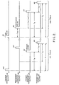
- Figure 1 illustrates the preferred embodiment of the invention as it might be practiced in the radar art.
- a conventional radar modulator and transmitter 10 is shown in block diagram form in Figure 1 coupled through a pulse transformer 11 to a magnetron transmitting tube 13.
- the magnetron transmitting tube feeds a radar antenna 15 in the usual fashion.
- Figure 1 also shows a conventional trigger generator 12 and a number of peripheral devices 14 of the type which require a pretrigger, such as electronic counter measure (ECM) devices, or signal processing circuits, for example.
- ECM electronic counter measure
- the trigger generator 12 is such as might be connected directly to the radar modulator and transmitter 10 is conventional radar circuits for providing a trigger pulse to fire the radar.
- radar modulators conventionally have an inherent component delay so that the burst of radio frequency engergy delivered to the antenna is not emitted until some finite time after the trigger pulse is applied to the modulator.
- This time delay is dependent upon a number of factors including temperature, humidity, and component aging, as well as upon the modulator and transmitter circuit design. Thus the time delay may vary widely from environment to environment and from radar to radar.
- the conventional radar also includes trigger pickoff circuitry 17 which is usually coupled to sense the modulator signal applied to the magnetron transmitting tube. The pickoff circuitry provides a signal substantially coincident with the burst of RF energy radiated through the antenna 15 and is therefore indicative that the radar transmitter has fired.
- the present invention is inserted between the trigger generator 12 and the radar modulator and transmitter 10, and is also connected to the peripheral devices 14 as shown in Figure 1.
- the invention comprises a system clock 16 for providing a succession of clock pulses which serve as a time base for sequencing and counting operations.
- a first counter referred to hereinafter as the modulator delay counter 18, is coupled to the system clock via a lead 20 and is also coupled via a lead 22 to the output of a first flip flop, hereinafter referred to as the modulator delay flip flop 24.
- a second counter, hereinafter referred to as the pretrigger counter 26 receives the clock pulses on a lead 28 and is also coupled to the output of a second flip flop, designated as the pretrigger flip flop 30, via a lead 32.
- a third counter, designated as the trigger counter 34 receives the clock pulses on a lead 36 and is coupled to output of a third flip flop or trigger flip flop 38 via a lead 40.
- Each of the three counters are preferably binary counters which count clock pulses when enabled by their respective flip flops 24, 30 and 38. They may be configured to count in straight binary, in binary coded decimal (BCD), or in some other numbering system.
- the output of the modulator delay counter 18, which may consist of a plurality of digits representing a time delay value, is carried via a parallel data bus 42 to the input of the pretrigger counter 26.
- the output of pretrigger counter 26 is also coupled via a lead 45 to the reset of R terminal of the pretrigger flip flop 30.
- the output of the trigger counter 34 which may be a modulator trigger pulse, for example, is carried via a lead 46 to the input of the radar modulator and transmitter 10.
- the output of the trigger counter 34 is also coupled via a lead 52 to the set of S terminal of the modulator delay flip flop 24, and is also coupled via a lead 54 to the reset of R terminal of the trigger flip flop 38.
- the trigger counter 34 is also supplied with a timing adjustment signal derived from a timing adjustment control 48 which provides a plurality of digits representing a desired time delay which are carried via a parallel data bus 50 to the trigger counter 34.
- the timing adjustment control 48 may be, for example, a thumb wheel device adapted for rotary adjustment by the operator and providing a digital output representative of the relative rotary position of the thumb wheel. If manual adjustment of the timing is not desired, the fixed digital number representing a fixed time delay may be hard wired to the trigger counter 34.
- the output of the trigger generator 12 is coupled via a lead 53 to the set or S terminal of the pretrigger flip flop 30, and via a lead 60 to the set or S terminal of the trigger flip flop 38.
- the output of trigger pickoff circuitry 17 is coupled via a lead 62 to the reset or R terminal of the modulator delay flip flop 24.
- line A of Figure 2 depicts the output of the trigger generator 12 which comprises a reference pulse 80 occurring once during each cycle of circuit operation. Each cycle of operation may be considered as beginning with a first such reference pulse 80 and ending with the next succeeding reference pulse.
- Line B of Figure 2 depicts the output of the pretrigger counter 26 which comprises a pulse 82.
- Line C of Figure 2 depicts the output of the trigger counter 34 which comprises a pulse 84 during each cycle of circuit operation.
- Line D of Figure 2 depicts the output signal of the trigger pickoff circuitry 17 which comprises an output pulse 86 indicative that the radar has fired.
- the output of the trigger generator 12 would normally be applied to the radar modulator 10 which would in turn trigger the radar to fire after a finite time delay through the modulator circuitry.
- the present invention utilises the output of the trigger generator 12 as a reference pulse and generates a p retrigger and trigger pulse after preselected time delays.
- the modulator delay counter 18, the pretri g ger counter 26, and the trigger counter 34 have been reset or initialised at some value as will be discussed more fully below. It will further be assumed that the logical state of the respective enable leads 22, 32, and 40 are such that none of the counters are initially enabled. Further it will be assumed that the timing adjustment control 40 has been preset by the operator and contains a plurality of digits representative of a desired time delay between the generation of a pretrigger pulse and the firing of the radar transmitter. These digits are coupled to the trigger counter 34 through the parallel data bus 50 and may be considered as an initial condition for the counting operation of the trigger counter 34. Finally, it will be assumed that the modulator delay counter 18 has been reset to some initial, preferably zero, value.
- the pretrigger counter 26 is initially set to a value received on the data bus 42 from the modulator delay counter 18. This initial value is established during the immediately preceding operational cycle. Thus during the first cycle of operation after system turn on, the numerical value on the data bus 42 may be treated as spurious and therefore disregarded. This may be accomplished in practice by including in the peripheral devices a logic circuit which ignores the first pretrigger pulse on lead 44 after system turn on. Other techniques for ignoring the initial pretrigger pulse will be apparent to those skilled in the art.
- the pretrigger flip flop 30 and the trigger flip flop 38 are set and the logical states of their respective enable leads 32 and 40 change.
- the pretrigger counter 26 and the trigger counter 34 then begin counting in synchronism with the system clock 16. Counting proceeds from the initial condition to which the pretrigger counter and trigger counter have been set via the data bus 42 and the data bus 50, respectively. When a preselected terminal condition is reached, the counting stops, and a pulse is emitted.
- the counters might be configured to count backwards from the initial condition to zero, wherein zero would represent the terminal count value.
- the counting may be either forwards or backwards and the terminal count may be any number such that a time delay is generated between the occurrence of a reference pulse 80 and the pretrigger and trigger pulses emitted from the respective counters when the respective terminal counts are reached.
- the time delay so generated may be computed according to the following formula, wherein t d is the time delay, f is the frequency of the clock, and n i and n t represent the initial and terminal numerical counts.
- the trigger counter 34 counts in synchronism with the system clock 16 from the initial condition set, via the timing adjustment control 48 to the terminal count, preferably zero.
- the trigger counter emits a pulse 84.
- the trigger counter pulse 84 is delayed a time t fd from the trigger generator output pulse or reference pulse 80, as shown on line C of Figure 2. As discussed above, this time delay t fd depends on the numerical spread between the initial and final numerical counts and upon the clock frequency.
- the pretrigger counter 26 counts in synchronism with the system clock 16. However, during the first cycle of operation after system turn on, the initial condition of the pretrigger counter 26 is considered spurious. When the pretrigger counter 26 reaches its terminal condition, a pretrigger pulse is emitted. Since this first pretrigger pulse is based on what is to be considered a spurious initial condition, it is to be ignored by the peripheral equipment 14. This first pretrigger pulse is shown on line B of Figure 2 and is given the reference numeral 82'; its position with respect to the reference pulse 80 is strictly arbitrary and is shown on line B for illustration purposes only.
- the trigger counter pulse 84 is applied on the lead 54 to the reset terminal R of the trigger counter flip flop 38, causing the flip flop state to change, thereby disabling and resetting the trigger counter 34.
- the trigger counter pulse 84 is also applied on the lead 46 to the radar modulator 10, thus triggering the latter in the usual fashion causing the radar modulator to fire after some finite time delay.
- This firing event is sensed by the trigger pickoff circuitry 17 which provides an output pulse 86 shown on line D in Figure 2.
- the pulse 86 will be seen to be delayed a time t md from the trigger counter pulse 84.
- This time delay t md is the inherent time delay characteristic of the particular radar modulator, which is known to vary from transmitter to transmitter and with changes in temperature, humidity, prime power fluctuations, and the like.
- the trigger counter pulse 84 is also applied on the lead 52 to the set of S terminal of the modulator delay flip flop 24, causing the logical state on the enable lead 22 to change, thereby enabling the modulator delay counter 18.
- the modulator delay counter 18 begins to count in synchronism with the system clock 16.
- the pulse 86 indicative of this event, is coupled through the lead 62 to the reset or R terminal of the modulator flip flop delay 24.
- the modulator delay counter 18 When the reset terminal of the flip flop 24 is activated, the modulator delay counter 18 is disabled, holding the count obtained just prior to being disabled. This count is transferred on the parallel data bus 42 to the pretrigger counter 26. It will be seen that the count is a measure of the time delay tmd generated by the radar modulators circuitry, and is applied to the pretrigger counter 26 as an initial condition for the succeeding cycle of operation.
- the second cycle of operation is shown on the right-hand side of Figure 2.
- the output pulse or reference pulse 80 of the trigger generator 12 is applied to the pretrigger flip flop 30 and to the trigger flip flop 38, which enables the pretrigger counter 26 and the trigger counter 34.
- Both counters 26 and 34 begin counting in synchronism with the system clock as discussed above.
- the pretrigger counter 26 When enabled, the pretrigger counter 26 begins to count starting with the initial condition which was set therein via the parallel data bus 42 during the first cycle of operation. When the pretrigger counter 26 reaches its terminal count, it emits a pretrigger pulse 82 which is carried on the lead 44 to the peripheral devices 14 and also carried on the lead 45 to be reset for R terminal of the flip flop 30. This resets the flip flop 30 which disables the pretrigger counter 26 from further counting. As shown on line B of Figure 2, the pretrigger pulse 82 occurs a time t md after the reference pulse 80, this being identical to the radar modulator delay time which was measured by the modulator delay counter 18 during the previous cycle of operation.
- the trigger counter 34 begins to count starting with the initial condition set therein by the timing adjustment control 48 via the data bus 50.
- the trigger counter emits a pulse 84 which is seen on line C of Figure 2 to occur a time t fd after the reference pulse 80.
- the trigger pulse 84 occurs a time t fd - t md after the pretrigger pulse 82.
- the trigger pulse 84 simultaneously triggers the radar modulator 10, enables the modulator delay counter 18, and resets the trigger counter 34.
- the radar modulator 10 again fires as illustrated by the pulse 86 on line D of Figure 2, which pulse is seen to be a time T after the reference pulse 80 which initiated that cycle.
- the trigger pulse 84 occurs a time t fd - t md after the pretrigger pulse 82, and with reference to line D of Figure 2, it will be seen that the radar modulator 10 fires, concurrent with pulse 86, a time t fd after the -pretrigger pulse 82.
- the operator can effectively control the timing of the pretrigger pulse 82 with respect to the firing of the radar modulator by adjusting the time t fd selected by the timing adjustment control 48.
- the circuit of the present invention provides in the illustrated embodiment a pretrigger pulse for use with peripheral equipment and also provides a radar trigger pulse.
- the circuit makes a dynamic measurement for each timing cycle of the inherent radar time delay t md which is used to insure against timing errors in the pretrigger which can arise on account of component aging or climatic changes.
- the inherent radar time delay is measured and compensated for the invention for by the invention thus eliminating the need to adjust the pretrigger circuitry to each individual radar transmitter.
- the circuit also permits the operator to vary or preselect the occurrence of the pretrigger pulse in relation to the modulator being triggered. This may be done from a remote location, for instance.
Landscapes
- Engineering & Computer Science (AREA)
- Computer Networks & Wireless Communication (AREA)
- Physics & Mathematics (AREA)
- General Physics & Mathematics (AREA)
- Radar, Positioning & Navigation (AREA)
- Remote Sensing (AREA)
- Radar Systems Or Details Thereof (AREA)
- Pulse Circuits (AREA)
- Oscillators With Electromechanical Resonators (AREA)
- Electrical Discharge Machining, Electrochemical Machining, And Combined Machining (AREA)
Applications Claiming Priority (2)
| Application Number | Priority Date | Filing Date | Title |
|---|---|---|---|
| US352484 | 1982-02-25 | ||
| US06/352,484 US4517567A (en) | 1982-02-25 | 1982-02-25 | Radar trigger and pretrigger generator having delay sensing and compensating circuit |
Publications (3)
| Publication Number | Publication Date |
|---|---|
| EP0087874A2 true EP0087874A2 (de) | 1983-09-07 |
| EP0087874A3 EP0087874A3 (en) | 1984-09-05 |
| EP0087874B1 EP0087874B1 (de) | 1988-06-29 |
Family
ID=23385314
Family Applications (1)
| Application Number | Title | Priority Date | Filing Date |
|---|---|---|---|
| EP83300686A Expired EP0087874B1 (de) | 1982-02-25 | 1983-02-11 | Vorrichtung und Verfahren zur Erzeugung von Vor-Auslöse und Auslösesignalen |
Country Status (6)
| Country | Link |
|---|---|
| US (1) | US4517567A (de) |
| EP (1) | EP0087874B1 (de) |
| JP (1) | JPS58148979A (de) |
| CA (1) | CA1203872A (de) |
| DE (1) | DE3377234D1 (de) |
| NO (1) | NO160631C (de) |
Families Citing this family (3)
| Publication number | Priority date | Publication date | Assignee | Title |
|---|---|---|---|---|
| EP1416633B1 (de) * | 2002-10-28 | 2012-12-05 | Rosemount Tank Radar AB | Schaltung und Verfahren zur Erzeugung von Triggersignalen |
| US7586433B1 (en) * | 2007-03-26 | 2009-09-08 | Mala Geoscience Ab | Dual port memory trigger system for a ground penetrating radar |
| US8150325B1 (en) | 2008-06-12 | 2012-04-03 | The United States Of America As Represented By The Secretary Of The Navy | Blanking system |
Family Cites Families (8)
| Publication number | Priority date | Publication date | Assignee | Title |
|---|---|---|---|---|
| GB676253A (en) * | 1950-02-16 | 1952-07-23 | Derek Anthony Underwood Rush | Improvements in or relating to pulse-synchronising circuits |
| US2955263A (en) * | 1956-11-30 | 1960-10-04 | Photographic Survey Corp Ltd | Thyratron modulator for short pulse radar and the like |
| US2946021A (en) * | 1958-02-10 | 1960-07-19 | Melvin P Siedband | Pulsing circuit for magnetron |
| US3465338A (en) * | 1968-05-15 | 1969-09-02 | Us Air Force | System for synchronizing a plurality of transmitters |
| JPS5612828B1 (de) * | 1970-03-10 | 1981-03-24 | ||
| US3950704A (en) * | 1974-09-12 | 1976-04-13 | The United States Of America As Represented By The Secretary Of The Navy | Video retimer system |
| US4083007A (en) * | 1976-09-20 | 1978-04-04 | International Telephone And Telegraph Corporation | Radar transmitter temporal noise reduction system |
| US4250454A (en) * | 1979-03-26 | 1981-02-10 | International Telephone And Telegraph Corporation | Electronic trigger for a radio frequency source |
-
1982
- 1982-02-25 US US06/352,484 patent/US4517567A/en not_active Expired - Lifetime
- 1982-12-07 CA CA000417212A patent/CA1203872A/en not_active Expired
-
1983
- 1983-01-10 JP JP58002132A patent/JPS58148979A/ja active Pending
- 1983-02-11 DE DE8383300686T patent/DE3377234D1/de not_active Expired
- 1983-02-11 EP EP83300686A patent/EP0087874B1/de not_active Expired
- 1983-02-24 NO NO830650A patent/NO160631C/no unknown
Also Published As
| Publication number | Publication date |
|---|---|
| NO160631C (no) | 1989-05-10 |
| DE3377234D1 (en) | 1988-08-04 |
| NO160631B (no) | 1989-01-30 |
| US4517567A (en) | 1985-05-14 |
| EP0087874B1 (de) | 1988-06-29 |
| NO830650L (no) | 1983-08-26 |
| CA1203872A (en) | 1986-04-29 |
| EP0087874A3 (en) | 1984-09-05 |
| JPS58148979A (ja) | 1983-09-05 |
Similar Documents
| Publication | Publication Date | Title |
|---|---|---|
| US5148175A (en) | High resolution variable range gate generator with programmable timing | |
| US2851596A (en) | Electronic counter | |
| EP0244052A2 (de) | Programmierbare Abtastablenkschaltung | |
| US3082374A (en) | Automatic testing system and timing device therefor | |
| US5367200A (en) | Method and apparatus for measuring the duty cycle of a digital signal | |
| EP0103393A1 (de) | Fahrzeug-Detektor mit Induktivschleife | |
| US4362988A (en) | Method of and circuit arrangement for determining the magnitude of an unknown resistance element | |
| US5637994A (en) | Waveform measurement | |
| GB2190774A (en) | Digital time delay | |
| EP0087874B1 (de) | Vorrichtung und Verfahren zur Erzeugung von Vor-Auslöse und Auslösesignalen | |
| GB1599258A (en) | Method of and system for evaluating received radar pulse trains | |
| US4654810A (en) | Facility for determining delay variations | |
| US2802105A (en) | Wave selecting and synchronizing system | |
| EP0182999B1 (de) | Selbsteinschaltendes, voruntersetzendes Frequenzzählersystem | |
| US2938202A (en) | Distance measuring apparatus | |
| US3965431A (en) | Circuitry for producing pulses with precise predetermined widths | |
| US3305859A (en) | Function generator for radar stc circuits | |
| US3979749A (en) | Range readout apparatus | |
| US3040260A (en) | Coded pulse train spacing tolerance checker | |
| US2939915A (en) | Pulse measurement | |
| US2558358A (en) | Timing method | |
| SU1240211A1 (ru) | Радиолокационный измеритель толщины лед ного покрова (его варианты) | |
| US4728816A (en) | Error and calibration pulse generator | |
| JPS6211556B2 (de) | ||
| US2790075A (en) | Delayed-pulse generating system |
Legal Events
| Date | Code | Title | Description |
|---|---|---|---|
| PUAI | Public reference made under article 153(3) epc to a published international application that has entered the european phase |
Free format text: ORIGINAL CODE: 0009012 |
|
| AK | Designated contracting states |
Designated state(s): DE GB IT NL |
|
| PUAL | Search report despatched |
Free format text: ORIGINAL CODE: 0009013 |
|
| AK | Designated contracting states |
Designated state(s): DE GB IT NL |
|
| 17P | Request for examination filed |
Effective date: 19850129 |
|
| 17Q | First examination report despatched |
Effective date: 19861204 |
|
| ITF | It: translation for a ep patent filed | ||
| GRAA | (expected) grant |
Free format text: ORIGINAL CODE: 0009210 |
|
| AK | Designated contracting states |
Kind code of ref document: B1 Designated state(s): DE GB IT NL |
|
| REF | Corresponds to: |
Ref document number: 3377234 Country of ref document: DE Date of ref document: 19880804 |
|
| PGFP | Annual fee paid to national office [announced via postgrant information from national office to epo] |
Ref country code: LU Payment date: 19890125 Year of fee payment: 7 |
|
| ITTA | It: last paid annual fee | ||
| PGFP | Annual fee paid to national office [announced via postgrant information from national office to epo] |
Ref country code: NL Payment date: 19890228 Year of fee payment: 7 |
|
| RAP2 | Party data changed (patent owner data changed or rights of a patent transferred) |
Owner name: SPERRY MARINE INC. |
|
| NLT2 | Nl: modifications (of names), taken from the european patent patent bulletin |
Owner name: SPERRY MARINE INC. TE CHARLOTTESVILLE, VIRGINIE, V |
|
| PLBE | No opposition filed within time limit |
Free format text: ORIGINAL CODE: 0009261 |
|
| STAA | Information on the status of an ep patent application or granted ep patent |
Free format text: STATUS: NO OPPOSITION FILED WITHIN TIME LIMIT |
|
| ITPR | It: changes in ownership of a european patent |
Owner name: CAMBIO RAGIONE SOCIALE;SPERRY MARINE INC. |
|
| PGFP | Annual fee paid to national office [announced via postgrant information from national office to epo] |
Ref country code: DE Payment date: 19890711 Year of fee payment: 7 |
|
| PGFP | Annual fee paid to national office [announced via postgrant information from national office to epo] |
Ref country code: GB Payment date: 19890731 Year of fee payment: 7 |
|
| 26N | No opposition filed | ||
| PG25 | Lapsed in a contracting state [announced via postgrant information from national office to epo] |
Ref country code: GB Effective date: 19900211 |
|
| PG25 | Lapsed in a contracting state [announced via postgrant information from national office to epo] |
Ref country code: NL Effective date: 19900901 |
|
| GBPC | Gb: european patent ceased through non-payment of renewal fee | ||
| NLV4 | Nl: lapsed or anulled due to non-payment of the annual fee | ||
| PG25 | Lapsed in a contracting state [announced via postgrant information from national office to epo] |
Ref country code: DE Effective date: 19901101 |