EP1416633B1 - Schaltung und Verfahren zur Erzeugung von Triggersignalen - Google Patents
Schaltung und Verfahren zur Erzeugung von Triggersignalen Download PDFInfo
- Publication number
- EP1416633B1 EP1416633B1 EP02024025A EP02024025A EP1416633B1 EP 1416633 B1 EP1416633 B1 EP 1416633B1 EP 02024025 A EP02024025 A EP 02024025A EP 02024025 A EP02024025 A EP 02024025A EP 1416633 B1 EP1416633 B1 EP 1416633B1
- Authority
- EP
- European Patent Office
- Prior art keywords
- pulse
- output
- width modulator
- monostable multivibrator
- edge
- Prior art date
- Legal status (The legal status is an assumption and is not a legal conclusion. Google has not performed a legal analysis and makes no representation as to the accuracy of the status listed.)
- Expired - Lifetime
Links
- 238000000034 method Methods 0.000 title claims description 19
- 230000001960 triggered effect Effects 0.000 claims description 7
- 230000001105 regulatory effect Effects 0.000 claims description 5
- 230000003111 delayed effect Effects 0.000 claims description 4
- 230000001276 controlling effect Effects 0.000 claims description 2
- 239000012530 fluid Substances 0.000 description 11
- 238000002592 echocardiography Methods 0.000 description 6
- 239000003990 capacitor Substances 0.000 description 3
- 230000001934 delay Effects 0.000 description 3
- 239000013078 crystal Substances 0.000 description 2
- 238000010586 diagram Methods 0.000 description 2
- 238000005259 measurement Methods 0.000 description 2
- 230000005540 biological transmission Effects 0.000 description 1
- 230000001419 dependent effect Effects 0.000 description 1
- 238000002347 injection Methods 0.000 description 1
- 239000007924 injection Substances 0.000 description 1
- 230000010354 integration Effects 0.000 description 1
- 238000001208 nuclear magnetic resonance pulse sequence Methods 0.000 description 1
- 238000005070 sampling Methods 0.000 description 1
- 238000006467 substitution reaction Methods 0.000 description 1
Images

Classifications
-
- G—PHYSICS
- G01—MEASURING; TESTING
- G01S—RADIO DIRECTION-FINDING; RADIO NAVIGATION; DETERMINING DISTANCE OR VELOCITY BY USE OF RADIO WAVES; LOCATING OR PRESENCE-DETECTING BY USE OF THE REFLECTION OR RERADIATION OF RADIO WAVES; ANALOGOUS ARRANGEMENTS USING OTHER WAVES
- G01S7/00—Details of systems according to groups G01S13/00, G01S15/00, G01S17/00
- G01S7/02—Details of systems according to groups G01S13/00, G01S15/00, G01S17/00 of systems according to group G01S13/00
- G01S7/03—Details of HF subsystems specially adapted therefor, e.g. common to transmitter and receiver
-
- G—PHYSICS
- G01—MEASURING; TESTING
- G01S—RADIO DIRECTION-FINDING; RADIO NAVIGATION; DETERMINING DISTANCE OR VELOCITY BY USE OF RADIO WAVES; LOCATING OR PRESENCE-DETECTING BY USE OF THE REFLECTION OR RERADIATION OF RADIO WAVES; ANALOGOUS ARRANGEMENTS USING OTHER WAVES
- G01S13/00—Systems using the reflection or reradiation of radio waves, e.g. radar systems; Analogous systems using reflection or reradiation of waves whose nature or wavelength is irrelevant or unspecified
- G01S13/02—Systems using reflection of radio waves, e.g. primary radar systems; Analogous systems
- G01S13/06—Systems determining position data of a target
- G01S13/08—Systems for measuring distance only
- G01S13/10—Systems for measuring distance only using transmission of interrupted, pulse modulated waves
- G01S13/18—Systems for measuring distance only using transmission of interrupted, pulse modulated waves wherein range gates are used
-
- G—PHYSICS
- G01—MEASURING; TESTING
- G01S—RADIO DIRECTION-FINDING; RADIO NAVIGATION; DETERMINING DISTANCE OR VELOCITY BY USE OF RADIO WAVES; LOCATING OR PRESENCE-DETECTING BY USE OF THE REFLECTION OR RERADIATION OF RADIO WAVES; ANALOGOUS ARRANGEMENTS USING OTHER WAVES
- G01S7/00—Details of systems according to groups G01S13/00, G01S15/00, G01S17/00
- G01S7/02—Details of systems according to groups G01S13/00, G01S15/00, G01S17/00 of systems according to group G01S13/00
- G01S7/28—Details of pulse systems
Definitions
- the present patent application relates to a timing circuit for generation of trigger signals for a radar level gauging system in accordance with the preamble of claim 1.
- the present patent application further relates to a method for generation of trigger signals for a radar level gauging system in accordance with the preamble of claim 6.
- the invention can be used to generate a reference transmit clock and a swept-delay receive clock for sampling-type fluid level sensing radar systems.
- Non-contact range measurement pulse-echo radar systems for fluid level sensing in tanks and vats typically consist of a transmitter which is arranged to radiate short duration radio frequency (RF) bursts via a highly directional antenna. After a delay a receiver is gated at a particular point in time. The timing of gating of the receiver is typically swept across a range of delays in a matter of milliseconds, such that a video output of the receiver can be provided as a scan like waveform. This waveform replicates occurring echoes on a real-time scale, corresponding to the physical distances represented by the echoes as the exact delay of a received echo pulse in relation to the transmitted pulse provides a measure of the distance to the reflecting object.
- RF radio frequency
- a precision digital pulse phase generator timing circuit is previously known through US 5,563,605 .
- This timing generator comprises a crystal oscillator connected to provide an output reference pulse.
- a resistor-capacitor combination is connected to provide a variable-delay output pulse from an input connected to the crystal oscillator.
- a phase monitor is connected to provide duty-cycle representations of the reference and variable-delay output pulse phase.
- An operational amplifier drives a control voltage to the resistor-capacitor combination according to currents integrated from the phase monitor and injected into summing junctions.
- a digital-to-analog converter injects a control current into the summing junctions according to an input digital control code.
- a servo equilibrium results that provides a phase delay of the variable-delay output pulse to the output reference pulse that linearly depends on the input digital control code.
- the timing circuit previously known through US 5,563,605 employs a NAND gate as a phase comparator in a delay locked loop configuration, which NAND gate must operate with sufficient clock timing difference to allow for the propagation of a sufficiently wide pulse through it.
- this previously known circuit has the disadvantage of having significant phase jitter or instability in the sample clock. This is a result of performance limitations of the high speed comparator required as part of the phase delay generator.
- Timing circuit for generation of trigger signals for a radar level gauging system comprising a pulse-width modulator, first and second integrators, a voltage summation element, a servo regulator, a reference clock output and a second clock output provided at the output of the pulse-width modulator.
- One object of the invention is to provide an improved timing circuit for generation of trigger signals for a radar level gauging system.
- a further object of the present invention is to provide an improved method for generation of trigger signals for a radar level gauging system.
- An advantage of the circuit and method in accordance with the present invention compared to prior art circuits and methods is that both the initial phase and the variable phase or delay difference between the triggering edges of the output signals are independently and accurately regulated to definable values, without having to rely on tolerances or matching of discrete components, such as resistors or capacitors.
- a further advantage of the circuit in accordance with the present invention is that relationship between the transmit clock and a swept-delay receive clock will remain the same, irrespective of external influences, such as ambient temperature, influencing the components thereof.
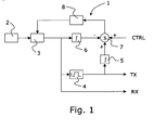
- Fig. 1 illustrates schematically a block diagram of a timing circuit according to a preferred embodiment of the present invention
- Fig. 2 is a simplified schematic view of how the timing circuit of figure 1 can be arranged to drive a radar level gauging system.
- the timing circuit 1 is arranged to provide a receiver control output clock pulse RX that is precisely delayed from a transmitter control output clock pulse TX according to a control signal input CTRL, e.g. a ramp sweep input signal. Further the RX and TX clock pulses are arranged to have the same frequency and a respective corresponding clock edge locked to each other.
- a transmitter In a radar fluid level sensing device, a transmitter generates a sequence of pulses which are directed towards a fluid surface, and the transmitter control output clock pulse TX control the transmitted pulses.
- a swept range gated receiver triggered by the receiver control output clock pulse RX, receives reflected signals from the fluid surface whereby the fluid level can be determined.
- the present invention is a precision high speed voltage controlled delay locked loop timing circuit 1 for generating trigger signals to be used in a device, such as a time domain fluid level sensing radar device, utilizing time expansion techniques where the triggering edge of the receiver control output clock pulse RX typically is swept linearly compared with the triggering edge of the transmitter control reference clock pulse TX.
- the linearity of the generated delay versus the control signal CTRL is ensured by using a simple servo regulator.
- the timing circuit 1 comprises an oscillator 2 arranged to output a pulse sequence, which oscillator 2 is connected to the input of a pulse width modulator 3.
- the pulse width modulator 3 having an input, an output and a control port and being responsive to a voltage at its control port for providing different pulse width output clock pulses triggered by the oscillator 2.
- the output of the pulse width modulator 3 provides a variable duty-cycle receiver control output clock RX.
- a monostable multivibrator 4 one-shot generator, has an input connected to the output of the pulse width modulator 3 and is arranged to be triggered by a leading edge of the clock pulse RX output by the pulse width modulator 3 to provide a fixed pulse width output clock pulse TX.
- the output of the monostable multivibrator 4 provides a constant duty-cycle transmitter control output clock TX.
- first and second independent integrators 5, 6 are connected to the outputs of the pulse width modulator 3 and the monostable multivibrator 4 respectively.
- These integrators 5, 6 can be realized as a pair of resistors providing for integration of the respective clock pulses RX and TX.
- the outputs of the first and second integrators 5, 6 are connected to a voltage summation element 7 and provides respective voltages that are proportional to the duty-cycles of the respective RX and TX clock pulses.
- the voltage summation element 7 is arranged to handle the voltages outputs by the first and second integrators 5, 6 with different signs (+/-), i.e. subtracting one from the other, as is evident from figure 1 .
- At least one control signal input CTRL is provided to the voltage summation element 7, allowing for injection of external control voltages.
- the output of the voltage summation element 7 provides a control loop to the control port of the pulse width modulator 3 via a servo regulator 8.
- the servo regulator 8 regulates the delay of the pulse width modulator 3 to balance the integrated voltages against any externally applied control voltages. The delay between the triggering edges of the TX and RX clock pulses is thereby precisely controlled by external control voltage inputs.
- the pulse width modulator 3 is arranged to output a variable duty cycle clock pulse, depending on the voltage provided to the control port thereof via the servo regulator 8. In the absence of control signal input voltages to the voltage summation element 7, the circuit 1 is arranged to stabilize such that the duty-cycle of a clock pulse RX output by the pulse-width modulator 3 precisely matches the duty cycle of a clock pulse TX output by the monostable multivibrator 4.
- the delay generation is indirectly accomplished by an independent proportional regulation of the duty-cycle level of the delayed output clock pulse RX while the initial delay or phase difference between the corresponding clock output edges is simultaneously and automatically regulated to zero.
- the initial delay or phase difference between the corresponding clock output edges can alternatively also be regulated to any desired positive or negative phase difference.
- the accuracy of the initial delay is ensured by the usage of the monostable multivibrator 4 generating a fixed pulse width that can be long enough not to cause any significant errors due to limitations in rise time and potential ringings.
- a suitable control signal CTRL is arranged to linearly control the skew time of the clock pulse RX output by the pulse-width modulator 3 from the clock pulse TX output by the monostable multivibrator 4.
- the triggering edge of the TX clock pulse is fixed and the triggering edge of the RX clock pulse sweeps through a range of delays.
- the duty-cycle of the clock pulse RX output by the pulse-width modulator 3 must adapt to maintain loop equilibrium.
- One such control signal usually is a linear ramp, e.g. a 0 to 5-volt linear ramp, derived e.g. from a precision linear ramp circuit.
- the circuit 1 provides a receiver gate triggering clock pulse RX that is precisely delayed from a transmitter triggering clock pulse TX output according to a control signal CTRL input value.
- FIG. 2 illustrates schematically how the timing circuit 1 can be arranged to drive a fluid level gauging radar system 9.
- the radar system 9 comprises a transmitter, a receiver and a directional antenna 10, which protrudes into a tank 11, the fluid level 12 of which is to be gauged.
- the reference clock output signal TX generated by the timing circuit 1 is used to control the transmitter to transmit a sequence of radio frequency (RF) bursts 13 via the antenna 10.
- the second clock output signal RX generated by the timing circuit 1 is used to control the gating of the receiver such that echoes 14 are sampled with different delays for each RF burst transmitted.
- RF radio frequency
- the timing circuit 1 enables the fluid level gauging radar system 9 to sweep the entire range to be gauged in order to obtain echo signals for each distance corresponding to the time difference between the transmission of an RF burst and the associated sampling of the receiver.
- a time expanded signal representing magnitude of the echoes obtained from the entire range can be produced, from which distances to echoes of interest easily can be obtained.
- a method for generation of trigger signals for a radar level gauging system comprises the steps of: providing a pulse-repetition-frequency clock pulse to a pulse width modulator 3; using an edge of an output clock pulse RX from the pulse width modulator 3 to trigger a monostable multivibrator 4 to output a fixed width clock pulse TX having one common edge with the output clock pulse RX from the pulse width modulator 3; obtaining average voltages related to the duty cycles of the output clock pulses RX, TX from the pulse width modulator 3 and the monostable multivibrator 4; controlling the delay of the output clock pulse RX from the pulse width modulator 3 with respect to the output clock pulse TX from the monostable multivibrator 4 by regulating the average voltages.
- the method further suggested to control the delay of the output clock pulse RX from the pulse width modulator 3 with respect to the output clock pulse TX from the monostable multivibrator 4 by applying a voltage ramp CTRL.
- the step of obtaining average voltages is performed by passing the output clock pulses RX, TX from the pulse width modulator 3 and the monostable multivibrator 4 through a respective integrator 5, 6.
- Delay of the output clock pulse RX from the pulse width modulator 3 with respect to the output clock pulse TX from the monostable multivibrator 4 is controlled by providing a control loop to a control port of the pulse width modulator 3.
- the method further comprises the step of applying the output RX and TX clock pulses to drive a radar level gauging system.
Landscapes
- Engineering & Computer Science (AREA)
- Radar, Positioning & Navigation (AREA)
- Remote Sensing (AREA)
- Computer Networks & Wireless Communication (AREA)
- Physics & Mathematics (AREA)
- General Physics & Mathematics (AREA)
- Radar Systems Or Details Thereof (AREA)
Claims (10)
- Zeitsteuerungsschaltung (1) zum Erzeugen von Triggersignalen für ein Radarpegelmesssystem, dadurch gekennzeichnet, dass es das Folgende umfasst:einen Impulsbreitenmodulator (3), welcher einen Eingang aufweist, der mit einem eine Impulswiederholungsfrequenz erzeugenden Oszillator (2) verbunden ist,einen monostabilen Multivibrator (4), welcher einen Eingang aufweist, der mit einem Ausgang des Impulsbreitenmodulators (3) verbunden ist,einen ersten und zweiten Integrator (5, 6), die mit einem Ausgang des Impulsbreitenmodulators (3) bzw. des monostabilen Multivibrators (4) verbunden sind,ein Spannungssummierungselement (7), welches mit einem Ausgang des ersten bzw. zweiten Integrators (5, 6) und mindestens einem Steuersignaleingang (CTRL) verbunden ist,einen Servoregulator (8), welcher eine Regelschleife zwischen einem Ausgang des Spannungssummierungselements (7) und einem Steueranschluss des Impulsbreitenmodulators (3) bereitstellt,einen Referenztaktausgang (TX), welcher am Ausgang des monostabilen Multivibrators (4) bereitgestellt ist, undeinen zweiten Taktausgang (RX), welcher am Ausgang Impulsbreitenmodulators (3) bereitgestellt ist.
- Schaltung (1) nach Anspruch 1, welche ferner dadurch gekennzeichnet ist, dass der monostabile Multivibrator (4) dafür eingerichtet ist, durch eine erste Impulsflanke einer Impulsausgabe (RX) durch den Impulsbreitenmodulator (3) dazu getriggert zu werden, einen Impuls fester Breite abzugeben.
- Schaltung (1) nach Anspruch 2, welche ferner dadurch gekennzeichnet ist, dass der Ausgang des monostabilen Multivibrators (4) dafür eingerichtet ist, den Zustand unmittelbar nach der Triggerung zu ändern und für eine feste Zeitdauer in diesem Zustand zu bleiben.
- Schaltung (1) nach einem der vorhergehenden Ansprüche, welche ferner dadurch gekennzeichnet ist, dass die zweite Impulsflanke einer Impulsausgabe (RX) durch den Impulsbreitenmodulator (3) dafür eingerichtet ist, ein Ausgangssignal mit verzögerter Flanke bereitzustellen, und die zweite Flanke der Ausgabe (TX) mit fester Impulsbreite durch den monostabilen Multivibrator (4) dafür eingerichtet ist, ein Ausgangssignal (TX) mit nicht verzögerter Referenzflanke bereitzustellen.
- Schaltung (1) nach einem der vorhergehenden Ansprüche, welche ferner dadurch gekennzeichnet ist, dass sie einen Radarsender, welcher dafür eingerichtet ist, von der Referenztaktausgabe (TX) getriggert zu werden, und einen Radarempfänger umfasst, welcher dafür eingerichtet ist, von der zweiten Taktausgabe (RX) getriggert zu werden.
- Verfahren zum Erzeugen von Triggersignalen für ein Radarpegelmesssystem, wobei das Verfahren dadurch gekennzeichnet ist, dass es die folgenden Schritte umfasst:Bereitstellen eines Impulsewiederholungsfrequenz-Taktimpulses für einen Impulsbreitenmodulator (3);Verwenden einer ersten Flanke eines Ausgangsimpulses (RX) aus dem Impulsbreitenmodulator (3), um einen monostabilen Multivibrator (4) dazu zu triggern, einen Impuls fester Breite (TX) auszugeben, welcher eine gemeinsame Flanke mit der ersten Flanke des Ausgangsimpulses (RX) aus dem Impulsbreitenmodulator (3) aufweist;Erhalten von mittleren Spannungen in Bezug auf die Tastgrade der Ausgangsimpulse (RX, TX) aus dem Impulsbreitenmodulator (3) und dem monostabilen Multivibrator (4);Steuern der Verzögerung des Ausgangsimpulses (RX) aus dem Impulsbreitenmodulator (3) in Bezug auf den Ausgangsimpuls (TX) aus dem monostabilen Multivibrator (4) durch Regulieren der mittleren Spannungen.
- Verfahren nach Anspruch 6, welches ferner dadurch gekennzeichnet ist, dass die Verzögerung des Ausgangsimpulses (RX) aus dem Impulsbreitenmodulator (3) in Bezug auf den Ausgangsimpuls (TX) aus dem monostabilen Multivibrator (4) durch Anwenden eines rampenförmigen Spannungsverlaufs (CTRL) gesteuert wird.
- Verfahren nach Anspruch 6 oder 7, welches ferner dadurch
gekennzeichnet ist, dass der Schritt des Erhaltens von mittleren Spannungen durch Leiten der Ausgangsimpulse (RX, TX) aus dem Impulsbreitenmodulator (3) und dem monostabilen Multivibrator (4) durch einen entsprechenden Integrator (5, 6) durchgeführt wird. - Verfahren nach einem der Ansprüche 6, 7 oder 8, welches ferner
dadurch gekennzeichnet ist, dass die Verzögerung des Ausgangsimpulses (RX) aus dem Impulsbreitenmodulator (3) in Bezug auf den Ausgangsimpuls (TX) aus dem monostabilen Multivibrator (4) durch Bereitstellen einer Regelschleife an einen Steueranschluss des Impulsbreitenmodulators (3) gesteuert wird. - Verfahren nach einem der Ansprüche 6, 7, 8 oder 9, welches ferner dadurch gekennzeichnet ist, dass es den Schritt des Verwenden der Ausgangsimpulse (RX, TX) zum Betreiben eines Radarpegelmesssystems umfasst.
Priority Applications (2)
| Application Number | Priority Date | Filing Date | Title |
|---|---|---|---|
| EP02024025A EP1416633B1 (de) | 2002-10-28 | 2002-10-28 | Schaltung und Verfahren zur Erzeugung von Triggersignalen |
| US10/281,280 US6700530B1 (en) | 2002-10-28 | 2002-10-28 | Circuit and method for generation of trigger signals |
Applications Claiming Priority (2)
| Application Number | Priority Date | Filing Date | Title |
|---|---|---|---|
| EP02024025A EP1416633B1 (de) | 2002-10-28 | 2002-10-28 | Schaltung und Verfahren zur Erzeugung von Triggersignalen |
| US10/281,280 US6700530B1 (en) | 2002-10-28 | 2002-10-28 | Circuit and method for generation of trigger signals |
Publications (2)
| Publication Number | Publication Date |
|---|---|
| EP1416633A1 EP1416633A1 (de) | 2004-05-06 |
| EP1416633B1 true EP1416633B1 (de) | 2012-12-05 |
Family
ID=32471888
Family Applications (1)
| Application Number | Title | Priority Date | Filing Date |
|---|---|---|---|
| EP02024025A Expired - Lifetime EP1416633B1 (de) | 2002-10-28 | 2002-10-28 | Schaltung und Verfahren zur Erzeugung von Triggersignalen |
Country Status (2)
| Country | Link |
|---|---|
| US (1) | US6700530B1 (de) |
| EP (1) | EP1416633B1 (de) |
Families Citing this family (18)
| Publication number | Priority date | Publication date | Assignee | Title |
|---|---|---|---|---|
| US7224944B2 (en) * | 2004-01-22 | 2007-05-29 | Mcewan Technologies, Llc | RF transceiver having a directly radiating transistor |
| US7595675B2 (en) * | 2006-05-01 | 2009-09-29 | International Business Machines Corporation | Duty cycle measurement method and apparatus that operates in a calibration mode and a test mode |
| US7330061B2 (en) * | 2006-05-01 | 2008-02-12 | International Business Machines Corporation | Method and apparatus for correcting the duty cycle of a digital signal |
| US7420400B2 (en) * | 2006-05-01 | 2008-09-02 | International Business Machines Corporation | Method and apparatus for on-chip duty cycle measurement |
| US7333905B2 (en) * | 2006-05-01 | 2008-02-19 | International Business Machines Corporation | Method and apparatus for measuring the duty cycle of a digital signal |
| US7363178B2 (en) * | 2006-05-01 | 2008-04-22 | International Business Machines Corporation | Method and apparatus for measuring the relative duty cycle of a clock signal |
| US7646177B2 (en) | 2006-05-01 | 2010-01-12 | International Business Machines Corporation | Design structure for a duty cycle measurement apparatus that operates in a calibration mode and a test mode |
| US8032850B2 (en) * | 2007-11-12 | 2011-10-04 | International Business Machines Corporation | Structure for an absolute duty cycle measurement circuit |
| US7904264B2 (en) | 2007-11-12 | 2011-03-08 | International Business Machines Corporation | Absolute duty cycle measurement |
| US7917318B2 (en) * | 2007-11-20 | 2011-03-29 | International Business Machines Corporation | Structure for a duty cycle measurement circuit |
| US7895005B2 (en) * | 2007-11-20 | 2011-02-22 | International Business Machines Corporation | Duty cycle measurement for various signals throughout an integrated circuit device |
| EP2068169B1 (de) * | 2007-12-06 | 2012-01-25 | Siemens Aktiengesellschaft | Impulsradarbewertungssystem |
| US8150325B1 (en) * | 2008-06-12 | 2012-04-03 | The United States Of America As Represented By The Secretary Of The Navy | Blanking system |
| US7952514B2 (en) * | 2008-11-20 | 2011-05-31 | Rosemount Tank Radar Ab | Energy storage unit for a radar level gauge system |
| US9121942B2 (en) * | 2012-11-05 | 2015-09-01 | Magnetrol International, Inc. | Guided wave radar delay lock loop circuit |
| US9291492B2 (en) * | 2013-03-12 | 2016-03-22 | Rosemount Tank Radar Ab | Tank feed through structure for a radar level gauge |
| US9593976B2 (en) * | 2014-05-19 | 2017-03-14 | Rosemount Tank Radar Ab | Pulsed level gauge system and method |
| KR102457467B1 (ko) * | 2017-12-12 | 2022-10-21 | 한국전자통신연구원 | 레이더 장치 |
Family Cites Families (18)
| Publication number | Priority date | Publication date | Assignee | Title |
|---|---|---|---|---|
| US4214240A (en) * | 1964-12-03 | 1980-07-22 | The United States Of America As Represented By The Secretary Of The Army | Coded pulse radar fuze |
| US3713145A (en) * | 1970-11-09 | 1973-01-23 | Motorola Inc | Pulse width control for radar transponders |
| US3792471A (en) * | 1972-05-08 | 1974-02-12 | K Kingsbury | Radar range lock loop |
| US5026156A (en) * | 1972-07-24 | 1991-06-25 | Martin Marietta Corporation | Method and system for pulse interval modulation |
| US4316193A (en) * | 1974-07-15 | 1982-02-16 | The Boeing Company | Servo loop processor |
| CA1118874A (en) * | 1976-08-13 | 1982-02-23 | Merle W. Faxon | Radar system with stable power output |
| US4517567A (en) * | 1982-02-25 | 1985-05-14 | Sperry Corporation | Radar trigger and pretrigger generator having delay sensing and compensating circuit |
| US4975703A (en) * | 1988-02-25 | 1990-12-04 | Lab-Volt (Quebec) Ltee/Ltd. | High resolution short range radar |
| US5614912A (en) * | 1991-09-09 | 1997-03-25 | The Mitre Corporation | Radar processing method and apparatus |
| US5586145A (en) * | 1993-01-11 | 1996-12-17 | Morgan; Harry C. | Transmission of electronic information by pulse position modulation utilizing low average power |
| US5563605A (en) | 1995-08-02 | 1996-10-08 | The Regents Of The University Of California | Precision digital pulse phase generator |
| US5926047A (en) | 1997-08-29 | 1999-07-20 | Micron Technology, Inc. | Synchronous clock generator including a delay-locked loop signal loss detector |
| US6055287A (en) | 1998-05-26 | 2000-04-25 | Mcewan; Thomas E. | Phase-comparator-less delay locked loop |
| US6191724B1 (en) | 1999-01-28 | 2001-02-20 | Mcewan Thomas E. | Short pulse microwave transceiver |
| US6072427A (en) | 1999-04-01 | 2000-06-06 | Mcewan; Thomas E. | Precision radar timebase using harmonically related offset oscillators |
| KR100346836B1 (ko) | 2000-06-07 | 2002-08-03 | 삼성전자 주식회사 | 듀티 사이클 보정 기능을 갖는 지연 동기 루프 회로 및지연 동기 방법 |
| US6504409B1 (en) * | 2001-04-17 | 2003-01-07 | K-Tek Corporation | Controller for generating a periodic signal with an adjustable duty cycle |
| US6853227B2 (en) * | 2001-04-17 | 2005-02-08 | K-Tek Corporation | Controller for generating a periodic signal with an adjustable duty cycle |
-
2002
- 2002-10-28 EP EP02024025A patent/EP1416633B1/de not_active Expired - Lifetime
- 2002-10-28 US US10/281,280 patent/US6700530B1/en not_active Expired - Fee Related
Also Published As
| Publication number | Publication date |
|---|---|
| EP1416633A1 (de) | 2004-05-06 |
| US6700530B1 (en) | 2004-03-02 |
Similar Documents
| Publication | Publication Date | Title |
|---|---|---|
| EP1416633B1 (de) | Schaltung und Verfahren zur Erzeugung von Triggersignalen | |
| EP0842564B1 (de) | Präziser digitaler pulsphasengenerator | |
| US7412337B2 (en) | Method for determining fill level on the basis of travel time of a high-frequency measuring signal | |
| Fitzgerald | Effects of range-Doppler coupling on chirp radar tracking accuracy | |
| US5023572A (en) | Voltage-controlled oscillator with rapid tuning loop and method for tuning same | |
| US6137438A (en) | Precision short-range pulse-echo systems with automatic pulse detectors | |
| US8390348B2 (en) | Time base generator and method for providing a first clock signal and a second clock signal | |
| US6864833B2 (en) | Time-base generator with self-compensating control loop | |
| US6373428B1 (en) | Self locking dual frequency clock system | |
| US20070192391A1 (en) | Direct digital synthesis radar timing system | |
| US20070210955A1 (en) | Error corrector for radar timing systems | |
| US20030025626A1 (en) | Pulse center detector for radars and reflectometers | |
| EP2207263B1 (de) | Digitaler Zeitablenkgenerator und Verfahren zum Bereitstellen eines ersten Taktsignals und eines zweiten Taktsignals | |
| US9031811B2 (en) | System and method for pulse-echo ranging | |
| US7548188B2 (en) | Precision radio frequency delay device | |
| JP4008046B2 (ja) | レーダシステム | |
| US5920288A (en) | Tracking system and method for controlling the field of view of a camera | |
| EP1631836B1 (de) | Verfahren und vorrichtung zur simulation eines dopplersignals zum selbst-test eines ruhenden höhenmessers | |
| US5266956A (en) | Method and device for the measurement of short distances by analysis of the delay in the propagation of a wave | |
| US5124708A (en) | RF stability measuring system for MTI radars | |
| US5055850A (en) | Waveform generator | |
| US5148178A (en) | Precision ranging system | |
| US6842139B1 (en) | Separation frequency detection in a radar level gauge | |
| CA2527725A1 (en) | Radar anti-fade systems and methods | |
| US6333710B1 (en) | Method for measuring the time delay between two periodic pulse signals of the same frequency |
Legal Events
| Date | Code | Title | Description |
|---|---|---|---|
| PUAI | Public reference made under article 153(3) epc to a published international application that has entered the european phase |
Free format text: ORIGINAL CODE: 0009012 |
|
| AK | Designated contracting states |
Kind code of ref document: A1 Designated state(s): AT BE BG CH CY CZ DE DK EE ES FI FR GB GR IE IT LI LU MC NL PT SE SK TR |
|
| AX | Request for extension of the european patent |
Extension state: AL LT LV MK RO SI |
|
| 17P | Request for examination filed |
Effective date: 20040916 |
|
| AKX | Designation fees paid |
Designated state(s): DE |
|
| 17Q | First examination report despatched |
Effective date: 20050217 |
|
| RAP1 | Party data changed (applicant data changed or rights of an application transferred) |
Owner name: SAAB ROSEMOUNT TANK RADAR AB |
|
| RAP1 | Party data changed (applicant data changed or rights of an application transferred) |
Owner name: ROSEMOUNT TANK RADAR AB |
|
| GRAP | Despatch of communication of intention to grant a patent |
Free format text: ORIGINAL CODE: EPIDOSNIGR1 |
|
| GRAC | Information related to communication of intention to grant a patent modified |
Free format text: ORIGINAL CODE: EPIDOSCIGR1 |
|
| GRAS | Grant fee paid |
Free format text: ORIGINAL CODE: EPIDOSNIGR3 |
|
| GRAA | (expected) grant |
Free format text: ORIGINAL CODE: 0009210 |
|
| AK | Designated contracting states |
Kind code of ref document: B1 Designated state(s): DE |
|
| REG | Reference to a national code |
Ref country code: DE Ref legal event code: R096 Ref document number: 60244150 Country of ref document: DE Effective date: 20130131 |
|
| PLBE | No opposition filed within time limit |
Free format text: ORIGINAL CODE: 0009261 |
|
| STAA | Information on the status of an ep patent application or granted ep patent |
Free format text: STATUS: NO OPPOSITION FILED WITHIN TIME LIMIT |
|
| 26N | No opposition filed |
Effective date: 20130906 |
|
| REG | Reference to a national code |
Ref country code: DE Ref legal event code: R097 Ref document number: 60244150 Country of ref document: DE Effective date: 20130906 |
|
| PGFP | Annual fee paid to national office [announced via postgrant information from national office to epo] |
Ref country code: DE Payment date: 20141029 Year of fee payment: 13 |
|
| REG | Reference to a national code |
Ref country code: DE Ref legal event code: R119 Ref document number: 60244150 Country of ref document: DE |
|
| PG25 | Lapsed in a contracting state [announced via postgrant information from national office to epo] |
Ref country code: DE Free format text: LAPSE BECAUSE OF NON-PAYMENT OF DUE FEES Effective date: 20160503 |