EP0085974A2 - Method of forming a number of solder portions on a semiconductor wafer - Google Patents
Method of forming a number of solder portions on a semiconductor wafer Download PDFInfo
- Publication number
- EP0085974A2 EP0085974A2 EP83101135A EP83101135A EP0085974A2 EP 0085974 A2 EP0085974 A2 EP 0085974A2 EP 83101135 A EP83101135 A EP 83101135A EP 83101135 A EP83101135 A EP 83101135A EP 0085974 A2 EP0085974 A2 EP 0085974A2
- Authority
- EP
- European Patent Office
- Prior art keywords
- solder
- semiconductor wafer
- regions
- foil
- forming
- Prior art date
- Legal status (The legal status is an assumption and is not a legal conclusion. Google has not performed a legal analysis and makes no representation as to the accuracy of the status listed.)
- Granted
Links
Images


Classifications
-
- H—ELECTRICITY
- H01—ELECTRIC ELEMENTS
- H01L—SEMICONDUCTOR DEVICES NOT COVERED BY CLASS H10
- H01L24/00—Arrangements for connecting or disconnecting semiconductor or solid-state bodies; Methods or apparatus related thereto
- H01L24/01—Means for bonding being attached to, or being formed on, the surface to be connected, e.g. chip-to-package, die-attach, "first-level" interconnects; Manufacturing methods related thereto
- H01L24/10—Bump connectors ; Manufacturing methods related thereto
- H01L24/11—Manufacturing methods
-
- H—ELECTRICITY
- H01—ELECTRIC ELEMENTS
- H01L—SEMICONDUCTOR DEVICES NOT COVERED BY CLASS H10
- H01L24/00—Arrangements for connecting or disconnecting semiconductor or solid-state bodies; Methods or apparatus related thereto
- H01L24/01—Means for bonding being attached to, or being formed on, the surface to be connected, e.g. chip-to-package, die-attach, "first-level" interconnects; Manufacturing methods related thereto
- H01L24/10—Bump connectors ; Manufacturing methods related thereto
- H01L24/12—Structure, shape, material or disposition of the bump connectors prior to the connecting process
- H01L24/13—Structure, shape, material or disposition of the bump connectors prior to the connecting process of an individual bump connector
-
- H—ELECTRICITY
- H01—ELECTRIC ELEMENTS
- H01L—SEMICONDUCTOR DEVICES NOT COVERED BY CLASS H10
- H01L2224/00—Indexing scheme for arrangements for connecting or disconnecting semiconductor or solid-state bodies and methods related thereto as covered by H01L24/00
- H01L2224/01—Means for bonding being attached to, or being formed on, the surface to be connected, e.g. chip-to-package, die-attach, "first-level" interconnects; Manufacturing methods related thereto
- H01L2224/10—Bump connectors; Manufacturing methods related thereto
- H01L2224/12—Structure, shape, material or disposition of the bump connectors prior to the connecting process
- H01L2224/13—Structure, shape, material or disposition of the bump connectors prior to the connecting process of an individual bump connector
- H01L2224/13001—Core members of the bump connector
- H01L2224/13099—Material
-
- H—ELECTRICITY
- H01—ELECTRIC ELEMENTS
- H01L—SEMICONDUCTOR DEVICES NOT COVERED BY CLASS H10
- H01L2924/00—Indexing scheme for arrangements or methods for connecting or disconnecting semiconductor or solid-state bodies as covered by H01L24/00
- H01L2924/0001—Technical content checked by a classifier
-
- H—ELECTRICITY
- H01—ELECTRIC ELEMENTS
- H01L—SEMICONDUCTOR DEVICES NOT COVERED BY CLASS H10
- H01L2924/00—Indexing scheme for arrangements or methods for connecting or disconnecting semiconductor or solid-state bodies as covered by H01L24/00
- H01L2924/01—Chemical elements
- H01L2924/01006—Carbon [C]
-
- H—ELECTRICITY
- H01—ELECTRIC ELEMENTS
- H01L—SEMICONDUCTOR DEVICES NOT COVERED BY CLASS H10
- H01L2924/00—Indexing scheme for arrangements or methods for connecting or disconnecting semiconductor or solid-state bodies as covered by H01L24/00
- H01L2924/01—Chemical elements
- H01L2924/01014—Silicon [Si]
-
- H—ELECTRICITY
- H01—ELECTRIC ELEMENTS
- H01L—SEMICONDUCTOR DEVICES NOT COVERED BY CLASS H10
- H01L2924/00—Indexing scheme for arrangements or methods for connecting or disconnecting semiconductor or solid-state bodies as covered by H01L24/00
- H01L2924/01—Chemical elements
- H01L2924/01015—Phosphorus [P]
-
- H—ELECTRICITY
- H01—ELECTRIC ELEMENTS
- H01L—SEMICONDUCTOR DEVICES NOT COVERED BY CLASS H10
- H01L2924/00—Indexing scheme for arrangements or methods for connecting or disconnecting semiconductor or solid-state bodies as covered by H01L24/00
- H01L2924/01—Chemical elements
- H01L2924/01024—Chromium [Cr]
-
- H—ELECTRICITY
- H01—ELECTRIC ELEMENTS
- H01L—SEMICONDUCTOR DEVICES NOT COVERED BY CLASS H10
- H01L2924/00—Indexing scheme for arrangements or methods for connecting or disconnecting semiconductor or solid-state bodies as covered by H01L24/00
- H01L2924/01—Chemical elements
- H01L2924/01032—Germanium [Ge]
-
- H—ELECTRICITY
- H01—ELECTRIC ELEMENTS
- H01L—SEMICONDUCTOR DEVICES NOT COVERED BY CLASS H10
- H01L2924/00—Indexing scheme for arrangements or methods for connecting or disconnecting semiconductor or solid-state bodies as covered by H01L24/00
- H01L2924/01—Chemical elements
- H01L2924/01033—Arsenic [As]
-
- H—ELECTRICITY
- H01—ELECTRIC ELEMENTS
- H01L—SEMICONDUCTOR DEVICES NOT COVERED BY CLASS H10
- H01L2924/00—Indexing scheme for arrangements or methods for connecting or disconnecting semiconductor or solid-state bodies as covered by H01L24/00
- H01L2924/01—Chemical elements
- H01L2924/01039—Yttrium [Y]
-
- H—ELECTRICITY
- H01—ELECTRIC ELEMENTS
- H01L—SEMICONDUCTOR DEVICES NOT COVERED BY CLASS H10
- H01L2924/00—Indexing scheme for arrangements or methods for connecting or disconnecting semiconductor or solid-state bodies as covered by H01L24/00
- H01L2924/01—Chemical elements
- H01L2924/01047—Silver [Ag]
-
- H—ELECTRICITY
- H01—ELECTRIC ELEMENTS
- H01L—SEMICONDUCTOR DEVICES NOT COVERED BY CLASS H10
- H01L2924/00—Indexing scheme for arrangements or methods for connecting or disconnecting semiconductor or solid-state bodies as covered by H01L24/00
- H01L2924/01—Chemical elements
- H01L2924/01057—Lanthanum [La]
-
- H—ELECTRICITY
- H01—ELECTRIC ELEMENTS
- H01L—SEMICONDUCTOR DEVICES NOT COVERED BY CLASS H10
- H01L2924/00—Indexing scheme for arrangements or methods for connecting or disconnecting semiconductor or solid-state bodies as covered by H01L24/00
- H01L2924/01—Chemical elements
- H01L2924/01061—Promethium [Pm]
-
- H—ELECTRICITY
- H01—ELECTRIC ELEMENTS
- H01L—SEMICONDUCTOR DEVICES NOT COVERED BY CLASS H10
- H01L2924/00—Indexing scheme for arrangements or methods for connecting or disconnecting semiconductor or solid-state bodies as covered by H01L24/00
- H01L2924/01—Chemical elements
- H01L2924/01082—Lead [Pb]
-
- H—ELECTRICITY
- H01—ELECTRIC ELEMENTS
- H01L—SEMICONDUCTOR DEVICES NOT COVERED BY CLASS H10
- H01L2924/00—Indexing scheme for arrangements or methods for connecting or disconnecting semiconductor or solid-state bodies as covered by H01L24/00
- H01L2924/013—Alloys
- H01L2924/014—Solder alloys
-
- H—ELECTRICITY
- H01—ELECTRIC ELEMENTS
- H01L—SEMICONDUCTOR DEVICES NOT COVERED BY CLASS H10
- H01L2924/00—Indexing scheme for arrangements or methods for connecting or disconnecting semiconductor or solid-state bodies as covered by H01L24/00
- H01L2924/10—Details of semiconductor or other solid state devices to be connected
- H01L2924/102—Material of the semiconductor or solid state bodies
- H01L2924/1025—Semiconducting materials
- H01L2924/10251—Elemental semiconductors, i.e. Group IV
- H01L2924/10253—Silicon [Si]
-
- H—ELECTRICITY
- H01—ELECTRIC ELEMENTS
- H01L—SEMICONDUCTOR DEVICES NOT COVERED BY CLASS H10
- H01L2924/00—Indexing scheme for arrangements or methods for connecting or disconnecting semiconductor or solid-state bodies as covered by H01L24/00
- H01L2924/10—Details of semiconductor or other solid state devices to be connected
- H01L2924/11—Device type
- H01L2924/12—Passive devices, e.g. 2 terminal devices
- H01L2924/1203—Rectifying Diode
- H01L2924/12036—PN diode
-
- H—ELECTRICITY
- H01—ELECTRIC ELEMENTS
- H01L—SEMICONDUCTOR DEVICES NOT COVERED BY CLASS H10
- H01L2924/00—Indexing scheme for arrangements or methods for connecting or disconnecting semiconductor or solid-state bodies as covered by H01L24/00
- H01L2924/10—Details of semiconductor or other solid state devices to be connected
- H01L2924/11—Device type
- H01L2924/12—Passive devices, e.g. 2 terminal devices
- H01L2924/1204—Optical Diode
- H01L2924/12042—LASER
-
- H—ELECTRICITY
- H01—ELECTRIC ELEMENTS
- H01L—SEMICONDUCTOR DEVICES NOT COVERED BY CLASS H10
- H01L2924/00—Indexing scheme for arrangements or methods for connecting or disconnecting semiconductor or solid-state bodies as covered by H01L24/00
- H01L2924/10—Details of semiconductor or other solid state devices to be connected
- H01L2924/11—Device type
- H01L2924/12—Passive devices, e.g. 2 terminal devices
- H01L2924/1204—Optical Diode
- H01L2924/12043—Photo diode
Definitions
- the present invention relates to an improvement of a method of forming a number of solder layers on one or both major surfaces of a semiconductor wafer.
- a drawback to be first mentioned is seen in the fact that the amount of deposited solder is uneven among the solder layers.
- the amount of solder deposited wettingly on the ohmic contacts will vary in dependence on an angle and a speed at which the semiconductor wafer is lifted or withdrawn upwardly from the molten solder bath as well as the temperature thereof.
- it is difficult to control the amount or quantity of solder deposited through wetting so that uniform thickness be attained for all the solder layers.
- a reduced quantity of the deposited solder will naturally result in a thin solder layer.
- a semiconductor device is to be constituted by a plurality of semiconductor elements disposed between rows of leads arrayed in opposition to each other with an equal distance between the leads in each row, which leads are attached to the respective semiconductor elements
- uneveness in the thickness of the solder layers will involve uneveness among the individual semiconductor elements in respect of the contact area over which the lead is contacted to the solder layer, whereby the thermal and the electrical characteristics are made unbalanced among the semiconductor elements.
- a second drawback resides in that the surface of the molten solder mass constituting the solder layer tends to be spherical under the surface tension.
- the lead to be attached may be inclined or positionally mis-aligned relative to the ohmic contact, providing an obstacle to attaining the desired structure of lead attachment. This problem is particularly serious when a plurality of semiconductor devices disposed between rows of the leads are to be attached with the leads.
- An object of the present invention is to provide a method of forming a number of discrete solder layers on a semiconductor wafer, in which the drawbacks of the prior art methods described above are eliminated.
- Another object of the present invention is to provide a method of forming a plurality of discrete solder layers on a semiconductor wafer, which solder layers are uniform in thickness and present flat top surfaces, respectively.
- a still further object of the present invention is to provide a method which is capable of forming a number of discrete solder layers on a semiconductor wafer having a uniformed thickness and presenting flat top surfaces with an improved reproducibility.
- a first feature of the method of forming discrete solder layers on a semiconductor wafer according to the invention resides in that those portions of one major surface of the semiconductor wafer having a large area on which the discrete solder layers are to be formed are rendered easier to be wetted with solder than the remaining portions, and a solder foil is disposed on the one major surface of the wafer to be subsequently heated. More specifically, those portions of the one major surface of the semiconductor wafer on which the solder layers are to be formed are provided with metal electrodes which can be ohmic-contacted to the semiconductor wafer and are easy to be wetted with solder, while at the remaining portions the surface of the semiconductor wafer is exposed as it is or alternatively coated with an insulation film.
- the solder foil After the solder foil has been disposed on the semiconductor wafer, the stacked structure or assembly is heated. As the consequence, molten solder is gathered on each of the metal electrodes under surface tension, whereby a number of separated or discrete solder layers are formed on the semiconductor wafer.
- the solder foil should preferably be realized in a net-like structure and disposed on the semiconductor wafer in such a manner that the center of each of meshes formed in the solder foil is located essentially at the center of an area defined by the adjacent metal electrodes among them, in order to assure the melting separation of the solder foil (i.e. separation of the solder foil into the discrete solder layers through melting of the former) in a satisfactory manner.
- the solder foil thus prepared is disposed on the semiconductor wafer to be subsequently subjected to the heating process.
- the solder foil prepared so as to meet the above geometrical or positional requirement is composed of solder foil portions provided in correspondence to the metal electrodes, respectively, and interconnecting portions or bridge portions for connecting or linking the solder foil portions to one another.
- the solder foil portion should preferably be of a slightly smaller area than that of the metal electrode so that solder material constituting the interconnection or bridge is also permitted to gather on the metal electrode when it is molten, to thereby assure the beakage of the interconnecting portion without fail. Further, it is preferred that the interconnecting bridge portion has a narrowed or constricted mid portion so that the breakage thereof through melting takes place at the well defined location, because the thickness of the solder layer as formed can then be made uniform more positively for all the metal electrodes.
- the step of separating or fragmenting the solder foil disposed on the semiconductor wafer into the discrete solder layers through melting is carried out in such a situation that the discrete solder layers may have a uniformed thickness and present respective flat top surfaces.
- a plate-like jig composed of a plate having a plurality of projections or protrusions which have a height equal to the thickness of the solder layer to be formed is disposed on the solder foil placed on the semiconductor wafer.
- the stacked assembly is subsequently heated to a melting temperature.
- the plate-like jig may be made of a material which is difficult to be wetted with solder and capable of withstanding the melting temperature of the solder material.
- the discrete solder layers will be formed simultaneously on a number of semiconductor wafers at both major surfaces thereof through the melting separation process.
- a single plate-like jig provided with the projections on both surfaces may be used for both the overlying and the underlying semiconductor wafers.
- the step of separating the solder foil disposed on the semiconductor wafer into the discrete solder layers through melting is carried out in non-oxidizing atmosphere. More specifically, the melting separation step is conducted in the atmosphere of an innert gas, a reducing gas or a gas mixture thereof.
- the melting separation step is carried out in the atmosphere of a reducing gas, the wettability to solder as well as the surface tension can be enhanced to allow the melting separation process to be effected smoothly.
- the finished solder layers present pure and clear surfaces, facilitating attachment of leads, to a further advantage.
- Figs. 1 to 5 are views which illustrate steps involved in carrying out the method according to a preferred embodiment of the invention.
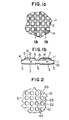
- a semiconductor wafer 1 of a large area in which a desired pn-juction is formed undergoes a treatment through which those portions of both major surfaces 11 and 12 of the semiconductor wafer 1 where solder layers are to be formed are rendered easy to be wetted with solder while the other portions being made difficult to be wetted with solder.
- a plurality of grooves 13 are formed in the one major surface 11 in such an array that the grooves 13 extend orthogonally in X- and Y-directions with the adjacent grooves being spaced at a substantially equal distance, whereby there are.produced a large number of mesa-like portions 14 each of a square surface in a matrix-like array, being partitioned from one another by the surrounding grooves.
- a metal electrode formed of a material exhibiting high wettability to the solder such as, for example, Ni, an alloy of Cr - Ni - Ag or the like.
- Similar metal electrodes 3 are also formed on the other major surface 12 of the semiconductor wafer 1 at locations corresponding to the mesa-like portions 14 in opposition thereto, respectively.
- the surfaces of the grooves 13 are covered with a passivation film 4 such as a glass film.
- the remaining portions of both the major surfaces are covered with a Si0 2 - film 5. Since the glass film 4 as well as the Si0 2 - film 5 is intrinsically poor in wettability to the solder, they are certainly effected in reducing the wettability to the solder at the portions covered with these films. It should however be noted that the inherent function of these films resides in passivating the active surfaces of the semiconductor surface. In other words, even when these portions of the semiconductor wafer are exposed as they are because of no passivation being required, the exposed surfaces can nevertheless be made difficult to be wetted with solder by virtue of the structure mentioned above.
- Fig. 2 illustrates a step for preparing a net-like solder foil 6 which has a uniform thickness and is provided with a number of circular or round meshes 61 formed and arrayed at the same pitch as the mesa-like portions 14 of the semiconductor wafer 1.
- the solder foil 6 may be considered to be constituted by a number of solder foil portions 62 arrayed in correspondence to the mesa-like portions 14 of the semiconductor wafer 1 and interconnecting portions or bridges 63 which connect the adjacent solder foil portions to one another.
- Each of the solder foil portions 62 is realized in an area smaller than that of the metal electrodes 2 and 3, while the interconnecting portion 63 is so formed as to present an intermediate portion of a reduced width as compared with the other portions thereof.
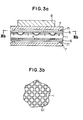
- Figs. 3a and 3b illustrate steps at which the solder foils 6 are positioned over both the major surfaces of the semiconductor wafer 1.
- a reference numeral 7 denotes a jig plate provided with a predetermined number of protrusions 71 each of a predetermined height.
- the solder foils 6 are positioned on both the major surfaces of the semiconductor wafer 1; respectively, in such a disposition that the solder foil portions 62 coincide with the metal electrodes 2 and 3, respectively, while the meshes 61 coincide, respectively, with those areas each defined among a quartet of the metal electrodes located adjacent to one another. More specifically, the solder foil 6 is positioned on the one major surface 11 of the semiconductor wafer 1 so that the meshes 61 coincide with the intersections of the grooves 13, respectively, while on the other major surface 12, the solder foil 6 is disposed so that the meshes 61 lie at locations which correspond to the projections of the said intersections on the other major surface 12, respectively.
- each of the meshes 61 is formed in such a size which allows the metal electrode (2; 3) to be partially exposed therethrough, when the solder foil 6 is disposed on the semiconductor wafer 1 in the manner described above.
- Each of the protrusions or projections 71 of the jig plate 7 has a height which is selected to be substantially equal to the thickness of the solder layer to be formed on the metal electrode (2; 3).
- the projections 71 are formed on the jig plate 7 at the positions which coincide with given ones of the metal electrodes (2; 3) or supporting studs formed previously on the semiconductor wafer 1.
- a reference numeral 8 denotes a load applying plate 8 disposed on the jig plate 7 for the purpose of preventing the semiconductor wafer 1 from being bent at a melting separation step described below.
- Figs. 4a to 4c are views for illustrating a manner in which the so-called melting separation of the solder foil 6 proceeds at the melting separation step which is carried out by heating up the laminated or stacked structure shown in Fig. 3 to a sufficiently high temperature for the solder foil 6 to be completely molten.
- the temperature in question lies in the range from 320°C to 450 o C when the solder being used is alloy of Pb - 5%Sn - 1.5%Ag.
- solder foil portions 62 being molten tend to spread over the respective underlying metal electrodes 2 due to the wettability thereof, while the interconnecting portions 63 tend to gather on the metal electrode 2 under the attraction exerted by a surface tension, as the result of which the state illustrated in Fig. 4b prevails in the solder foil 6.
- the interconnecting portions 63 are broken to be heaped on the metal electrodes, while gathered masses of the solder material spread wettingly all over the whole top surfaces of the metal electrodes 2, whereby the state illustrated in Fig. 4c is ultimately attained.
- the molten solder gathering on the metal electrode tends to become spherical under the surface tension. This tendency is however suppressed by the jig plate 7.
- a solder layer 9 having a flat top surface is obtained, as is shown in Fig. 5.
- the melting separation process described above should be carried out in a non-oxidizing atmosphere and more preferably in a reducing atmosphere such as hidrogen gas atmosphere.
- Fig. 5 shows the semiconductor wafer 1 provided with a number of the solder layers 9 formed on both the major surfaces through the steps elucidated above.
- the semiconductor wafer 1 thus finished is then cut along the grooves 13 with suitable means such as, for example, a laser beam into a number of semiconductor elements each of which is subsequently assembled to a semiconductor device after attachment of leads and air-tight sealing.
- Cince such assembling process is irrelevant to the essence of the present invention, description thereof will be unnecessary.
- a disc-like silicon wafer of 100mm in diameter was prepared. After formation of a pn-junction in this wafer, a number of the grooves each of 200 pm in width and 65 ⁇ m in depth were formed in one of the major surfaces of the wafer at a pitch of 1.9mm so that the grooves extend orthogonally in X- and Y- directions, as is shown in Fig. la, to thereby form a corresponding number of the mesa-like portions of 1.7 mm square in a juxtaposed array.
- the grooves were coated with a glass film of 5 ⁇ m in thickness.
- Metal electrodes of Cr - Ni - Ag each of 1.45 mm square and 2.2 ⁇ m thick were formed on the surface of the mesa-like portions, respectively.
- each metal electrode is coated with a Si0 2 - film in thickness of 1 pm.
- Metal electrodes of Cr - Ni - Ag each of 1.45 mm square and 2.2 pm thick were formed on the other major surface of the silicon wafer at positions corresponding to the mesa-like portions.
- the remaining portions of the other major surface was coated with a Si0 2 - film in thickness of 1 ⁇ m.
- a solder disc of Pb - Ag - Sn having a thickness of 100 ⁇ m and a diameter equal to that of the wafer was prepared.
- a number of through-holes each of 1.4 mm in diameter were formed in the solder disc in X- and Y- directions in a juxtaposed array at an inter-center pitch of 1.9 mm, to thereby form the so-called solder foil.
- Jig plates each composed of a disc having a thickness of 2.5 mm and a diameter equal to that of the wafer and a desired number (nine in this illustrated case) of projections of 100 pm in height formed on one or both surfaces of the disc were prepared.
- Five silicon war- fers were stacked with the solder foils and the jig plates being interposed in a laminated structure shown in Fig. 7.
- a load plate of 1.5 Kg was disposed on the top jig plate.
- the solder foil is molten and separated into the individual discrete solder layers formed on the metal electrodes, respectively. All the discrete solder layers formed on the metal electrodes were 100 um thick and presented flat surfaces of substantially same shape as those formed on the other major surface of the wafer.
Abstract
Description
- The present invention relates to an improvement of a method of forming a number of solder layers on one or both major surfaces of a semiconductor wafer.
- In fabrication of a semiconductor element of a small current capacity, it is generally adopted in practice that a single semiconductor wafer of a large area is first prepared in which a pn-junction is formed, which is followed by passivating treatment of the exposed portions of the pn-junction, provision of ohmic contacts and formation of solder layers on the ohmic contacts. Thereafter, the semiconductor wafer is divided into a number of semiconductor pellets from which the semiconductor elements are realized. This manufacturing method is certainly excellent in respect of the mass- productivity. There arise however problems in this manufacturing method in connection with the step of forming the solder layers.
- As a method of forming a number of discrete solder layers on the semiconductor wafer, it has heretofore been widely adopted that a semiconductor wafer provided with the ohmic contacts is immersed in a molten solder bath. This method in which difference in wettability to solder between the semiconductor and the ohmic contacts is taken advantage of is certainly a simple and convenient process for allowing the solder layers to be formed only on the ohmic contacts. However, this method suffers drawbacks which will be mentioned below.
- A drawback to be first mentioned is seen in the fact that the amount of deposited solder is uneven among the solder layers. The amount of solder deposited wettingly on the ohmic contacts will vary in dependence on an angle and a speed at which the semiconductor wafer is lifted or withdrawn upwardly from the molten solder bath as well as the temperature thereof. In the present state of the technical level, it is difficult to control the amount or quantity of solder deposited through wetting so that uniform thickness be attained for all the solder layers. A reduced quantity of the deposited solder will naturally result in a thin solder layer.
- In that case, when the pellet provided with such thin solder layer is assembled to a semiconductor device by attaching leads to the solder layers, significant stress is produced due to difference in thermal expansion between the semiconductor pellet and the lead attached to the solder layer, to thereby shorten the use life of the solder layer. On the contrary, deposition of solder in an excessive quantity results in formation of the solder layer of an increased thickness, increasing the heat resistance and electrical resistance of the solder layer, as the result of which thermal and electrical characteristics of the finished semiconductor device will inevitably be degraded. Further, in case a semiconductor device is to be constituted by a plurality of semiconductor elements disposed between rows of leads arrayed in opposition to each other with an equal distance between the leads in each row, which leads are attached to the respective semiconductor elements, uneveness in the thickness of the solder layers will involve uneveness among the individual semiconductor elements in respect of the contact area over which the lead is contacted to the solder layer, whereby the thermal and the electrical characteristics are made unbalanced among the semiconductor elements.
- A second drawback resides in that the surface of the molten solder mass constituting the solder layer tends to be spherical under the surface tension. When the surface of the molten solder layer becomes spherical, the lead to be attached may be inclined or positionally mis-aligned relative to the ohmic contact, providing an obstacle to attaining the desired structure of lead attachment. This problem is particularly serious when a plurality of semiconductor devices disposed between rows of the leads are to be attached with the leads.
- An object of the present invention is to provide a method of forming a number of discrete solder layers on a semiconductor wafer, in which the drawbacks of the prior art methods described above are eliminated.
- Another object of the present invention is to provide a method of forming a plurality of discrete solder layers on a semiconductor wafer, which solder layers are uniform in thickness and present flat top surfaces, respectively.
- A still further object of the present invention is to provide a method which is capable of forming a number of discrete solder layers on a semiconductor wafer having a uniformed thickness and presenting flat top surfaces with an improved reproducibility.
- In view of the objects mentioned above, a first feature of the method of forming discrete solder layers on a semiconductor wafer according to the invention resides in that those portions of one major surface of the semiconductor wafer having a large area on which the discrete solder layers are to be formed are rendered easier to be wetted with solder than the remaining portions, and a solder foil is disposed on the one major surface of the wafer to be subsequently heated. More specifically, those portions of the one major surface of the semiconductor wafer on which the solder layers are to be formed are provided with metal electrodes which can be ohmic-contacted to the semiconductor wafer and are easy to be wetted with solder, while at the remaining portions the surface of the semiconductor wafer is exposed as it is or alternatively coated with an insulation film. After the solder foil has been disposed on the semiconductor wafer, the stacked structure or assembly is heated. As the consequence, molten solder is gathered on each of the metal electrodes under surface tension, whereby a number of separated or discrete solder layers are formed on the semiconductor wafer. In conjunction with the first feature or aspect of the inventive method described above, the solder foil should preferably be realized in a net-like structure and disposed on the semiconductor wafer in such a manner that the center of each of meshes formed in the solder foil is located essentially at the center of an area defined by the adjacent metal electrodes among them, in order to assure the melting separation of the solder foil (i.e. separation of the solder foil into the discrete solder layers through melting of the former) in a satisfactory manner. In more concrete, when the metal electrodes of a same configuration are formed and disposed in a matrix-like array on the semiconductor wafer, the distance between any given meshes located adjacent to each other is so determined that each of the meshes lies among a given quartet of the adjacent metal electrodes. The solder foil thus prepared is disposed on the semiconductor wafer to be subsequently subjected to the heating process. In other words, it can be said that the solder foil prepared so as to meet the above geometrical or positional requirement is composed of solder foil portions provided in correspondence to the metal electrodes, respectively, and interconnecting portions or bridge portions for connecting or linking the solder foil portions to one another. The solder foil portion should preferably be of a slightly smaller area than that of the metal electrode so that solder material constituting the interconnection or bridge is also permitted to gather on the metal electrode when it is molten, to thereby assure the beakage of the interconnecting portion without fail. Further, it is preferred that the interconnecting bridge portion has a narrowed or constricted mid portion so that the breakage thereof through melting takes place at the well defined location, because the thickness of the solder layer as formed can then be made uniform more positively for all the metal electrodes.
- According to a second feature of the present invention, the step of separating or fragmenting the solder foil disposed on the semiconductor wafer into the discrete solder layers through melting is carried out in such a situation that the discrete solder layers may have a uniformed thickness and present respective flat top surfaces. To this end, a plate-like jig composed of a plate having a plurality of projections or protrusions which have a height equal to the thickness of the solder layer to be formed is disposed on the solder foil placed on the semiconductor wafer. The stacked assembly is subsequently heated to a melting temperature. The plate-like jig may be made of a material which is difficult to be wetted with solder and capable of withstanding the melting temperature of the solder material. In most of practical applications, the discrete solder layers will be formed simultaneously on a number of semiconductor wafers at both major surfaces thereof through the melting separation process. In such case, a single plate-like jig provided with the projections on both surfaces may be used for both the overlying and the underlying semiconductor wafers.
- According to a third feature of the solder layer forming method according to the present invention, the step of separating the solder foil disposed on the semiconductor wafer into the discrete solder layers through melting (i.e. the melting separation step or process) is carried out in non-oxidizing atmosphere. More specifically, the melting separation step is conducted in the atmosphere of an innert gas, a reducing gas or a gas mixture thereof. In particular, when the melting separation step is carried out in the atmosphere of a reducing gas, the wettability to solder as well as the surface tension can be enhanced to allow the melting separation process to be effected smoothly. Besides, the finished solder layers present pure and clear surfaces, facilitating attachment of leads, to a further advantage.
- The present invention will be more apparent from the following detailed description taken in conjunction with the accompanying drawings, in which:
- Fig. 1 to 5 are views for illustrating steps of a solder layer forming method according to a preferred embodiment of the invention;
- Figs. 6a and 6b are plan views showing modifications of a solder foil which can be used in carrying out the method according to the invention; and
- Fig. 7 snows in a schematic sectional view a version of the melting separation step involved in carrying out the method according to the invention.
- Now, the method of forming discrete solder layers according to the present invention will be described in detail in conjunction with its preferred embodiments by referring to the drawings.
- Figs. 1 to 5 are views which illustrate steps involved in carrying out the method according to a preferred embodiment of the invention.
- At steps illustrated in Figs. la and Ib, a semiconductor wafer 1 of a large area in which a desired pn-juction is formed undergoes a treatment through which those portions of both
major surfaces 11 and 12 of the semiconductor wafer 1 where solder layers are to be formed are rendered easy to be wetted with solder while the other portions being made difficult to be wetted with solder. To this end, a plurality of grooves 13 are formed in the one major surface 11 in such an array that the grooves 13 extend orthogonally in X- and Y-directions with the adjacent grooves being spaced at a substantially equal distance, whereby there are.produced a large number of mesa-like portions 14 each of a square surface in a matrix-like array, being partitioned from one another by the surrounding grooves. On each of the surfaces of the mesa-like portions 14, a metal electrode formed of a material exhibiting high wettability to the solder such as, for example, Ni, an alloy of Cr - Ni - Ag or the like.Similar metal electrodes 3 are also formed on the othermajor surface 12 of the semiconductor wafer 1 at locations corresponding to the mesa-like portions 14 in opposition thereto, respectively. The surfaces of the grooves 13 are covered with apassivation film 4 such as a glass film. Further, the remaining portions of both the major surfaces are covered with a Si02 -film 5. Since theglass film 4 as well as the Si02 -film 5 is intrinsically poor in wettability to the solder, they are certainly effected in reducing the wettability to the solder at the portions covered with these films. It should however be noted that the inherent function of these films resides in passivating the active surfaces of the semiconductor surface. In other words, even when these portions of the semiconductor wafer are exposed as they are because of no passivation being required, the exposed surfaces can nevertheless be made difficult to be wetted with solder by virtue of the structure mentioned above. - Fig. 2 illustrates a step for preparing a net-
like solder foil 6 which has a uniform thickness and is provided with a number of circular orround meshes 61 formed and arrayed at the same pitch as the mesa-like portions 14 of the semiconductor wafer 1. On account of the presence of themeshes 61, thesolder foil 6 may be considered to be constituted by a number ofsolder foil portions 62 arrayed in correspondence to the mesa-like portions 14 of the semiconductor wafer 1 and interconnecting portions orbridges 63 which connect the adjacent solder foil portions to one another. Each of thesolder foil portions 62 is realized in an area smaller than that of themetal electrodes portion 63 is so formed as to present an intermediate portion of a reduced width as compared with the other portions thereof. - Figs. 3a and 3b illustrate steps at which the
solder foils 6 are positioned over both the major surfaces of the semiconductor wafer 1. In Fig. 3a, areference numeral 7 denotes a jig plate provided with a predetermined number ofprotrusions 71 each of a predetermined height. The stacked or laminated structure in which the semiconductor wafer 1 sandwiched between two sheets of thesolder foil 6 is disposed between a pair of thejig plates 7 which are so positioned that therespective projections 71 faces each other in alignment. Referring to Fig. 3b, the solder foils 6 are positioned on both the major surfaces of the semiconductor wafer 1; respectively, in such a disposition that thesolder foil portions 62 coincide with themetal electrodes meshes 61 coincide, respectively, with those areas each defined among a quartet of the metal electrodes located adjacent to one another. More specifically, thesolder foil 6 is positioned on the one major surface 11 of the semiconductor wafer 1 so that themeshes 61 coincide with the intersections of the grooves 13, respectively, while on the othermajor surface 12, thesolder foil 6 is disposed so that themeshes 61 lie at locations which correspond to the projections of the said intersections on the othermajor surface 12, respectively. In this connection, it should be noted that each of themeshes 61 is formed in such a size which allows the metal electrode (2; 3) to be partially exposed therethrough, when thesolder foil 6 is disposed on the semiconductor wafer 1 in the manner described above. Each of the protrusions orprojections 71 of thejig plate 7 has a height which is selected to be substantially equal to the thickness of the solder layer to be formed on the metal electrode (2; 3). Theprojections 71 are formed on thejig plate 7 at the positions which coincide with given ones of the metal electrodes (2; 3) or supporting studs formed previously on the semiconductor wafer 1. In Fig. 3a, areference numeral 8 denotes aload applying plate 8 disposed on thejig plate 7 for the purpose of preventing the semiconductor wafer 1 from being bent at a melting separation step described below. - Figs. 4a to 4c are views for illustrating a manner in which the so-called melting separation of the
solder foil 6 proceeds at the melting separation step which is carried out by heating up the laminated or stacked structure shown in Fig. 3 to a sufficiently high temperature for thesolder foil 6 to be completely molten. The temperature in question lies in the range from 320°C to 450oC when the solder being used is alloy of Pb - 5%Sn - 1.5%Ag. When thesolder foil 6 of the initial configuration shown in Fig. 4a begins to be molten in the initial phase of this melting separation process, thesolder foil portions 62 being molten tend to spread over the respectiveunderlying metal electrodes 2 due to the wettability thereof, while the interconnectingportions 63 tend to gather on themetal electrode 2 under the attraction exerted by a surface tension, as the result of which the state illustrated in Fig. 4b prevails in thesolder foil 6. As the melting further proceeds, the interconnectingportions 63 are broken to be heaped on the metal electrodes, while gathered masses of the solder material spread wettingly all over the whole top surfaces of themetal electrodes 2, whereby the state illustrated in Fig. 4c is ultimately attained. In this case, the molten solder gathering on the metal electrode tends to become spherical under the surface tension. This tendency is however suppressed by thejig plate 7. Thus, asolder layer 9 having a flat top surface is obtained, as is shown in Fig. 5. The melting separation process described above should be carried out in a non-oxidizing atmosphere and more preferably in a reducing atmosphere such as hidrogen gas atmosphere. - Fig. 5 shows the semiconductor wafer 1 provided with a number of the solder layers 9 formed on both the major surfaces through the steps elucidated above. The semiconductor wafer 1 thus finished is then cut along the grooves 13 with suitable means such as, for example, a laser beam into a number of semiconductor elements each of which is subsequently assembled to a semiconductor device after attachment of leads and air-tight sealing.
- Cince such assembling process is irrelevant to the essence of the present invention, description thereof will be unnecessary.
- Advantageous effects involved in the method of forming the solder layers according to the teaching of the invention will be mentioned below:
- (1) By virtue of such provision that those portions of the major surfaces of the semiconductor wafer at which the solder layers are to be formed are rendered easily wettable with the molten solder material while the remaining portions being made difficult to be wetted, a number of the individual discrete solder layers can be realized through the single melting separation process merely by heating the solder foils disposed on the major surfaces of the semiconductor wafer. Assuming that the solder layers were connected to one another by the solder material to the contrary, the semiconductor pellets which are formed by mechanically cutting the semiconductor wafer provided with the interconnected solder layer would be inevitably polluted with the solder material at the cut faces, requiring thus troublesome and time consuming procedures for removing the pollution. The method of forming the discrete solder layers according to the preferred embodiment of the invention described above is immune to such difficulty.
- (2) Because the solder foil is realized in the net-like configuration in which the shapes and array of the portions of the semiconductor wafer to be provided with the solder layers is taken into account, the separation of the single solder foil into a number of the discrete solder layers by melting the foil (i.e. through the melting separation) can be smoothly and positively effected.
- (3) By virtue of such arrangement that the semiconductor foil of the net-like configuration includes a number of the solder foil portions positioned, respectively, on the metal electroces of the semiconductor wafer to be provided with the discrete solder layers, each portion having a slightly smaller area than that of the metal electrode, and the interconnecting bridges for linking the adjacent solder foil portions to one another, wherein each bridge is most reduced in width at the mid portion thereof, attraction of a relatively great strength :is available for pulling or gathering the molten solder mass forming the interconnection onto the metal electrodes, whereby the melting separation of the solder foil into the individual discrete solder layer can be effected without fail. Further, since the breakage of the interconnecting bridge through the melting necessarily occurs at the narrowest portion thereof, the amount of the molten solder material heaped up on the metal electrodes can be spontaneously made uniform throughout all the discrete solder layers.
- (4) Since the separation of the solder foil into the individual solder layers through the melting proceeds in the state in which the tendency of the molten solder material to become spherical under the surface tension is suppressed by the jig plate, the top surfaces of the solder layers can be flattened uniformly, involving no unevenness in level among the adjacent solder layers. Thus, the various problems arising in connection with the attachment of the leads to the semiconductor elements, as described hereinbefore, can be all disposed of in a satisfactory manner.
- (5) Because the melting separation of the solder foil is carried out in the non-oxidizing atmosphere and more preferably in the reducing atmosphere, the melting separation can take place smoothly with the surface of the solder layer being simultaneously purified.
- In the foregoing, the present invention has been described in conjunction with its preferred embodiment. The invention can moreover be carried out in various modified manners mentioned below:
- As a first modification, Figs. 6a and 6b show examples of the solder foil which may be used in carrying out the invention. In the case of the solder foil shown in Fig. 6a, the solder foil portion denoted by 62 is of a square shape like that of the metal electrode 2 (or 3). (The area of the former is however slightly smaller than the latter.) In this case, the interconnecting
bridge 63 should preferably be imparted with a reduced width at the mid portion thereof. In the case of the solder foil illustrated in Fig. 6b, the mesh is realized in a rectangular shape. In this connection, it should be mentioned that the solder foil having no meshes also may be used, although not shown. In that case, however, a lot of time will be involved in the melting separation. Besides, there is a possibility that the solder foil might not be divided perfectly into the individual solder layers. - A second conceivable modification concerns the semiconductor wafer. For example, a semiconductor wafer having the grooves formed in both the major surfaces, a semiconductor wafer provided with no grooves at both the major surfaces, a semiconductor wafer in which the metal electrode is round and the like may be equally employed.
- A third modification concerns the material of which the semiconductor wafer is made. The invention may be applied not only to the semiconductor wafer of silicon, but to those made of germanium, silicon carbide and a compound semiconductor, respectively.
- A fourth possible modification concerns the step illustrated in Fig. 3a, in which it is assumed that the solder layers are to be formed on the single semiconductor wafer. In case the solder layers are to be formed simultaneously on a plurality of semiconductor wafers, a desired number of the laminated structure illustrated in Fig. 3a may be stacked on one another. Alternatively, a plurality of the semiconductor wafers 1 may be stacked between the top and the
bottom jig plates 7, whereinjig plates 10 each havingprotrusions 101 and 102 formed at both surfaces and the solder foils 6 are interposed between the adjacent semiconductor wafers 1, as illustrated in Fig. 7. - Next, a numerical example of the invention will be mentioned below.
- A disc-like silicon wafer of 100mm in diameter was prepared. After formation of a pn-junction in this wafer, a number of the grooves each of 200 pm in width and 65 µm in depth were formed in one of the major surfaces of the wafer at a pitch of 1.9mm so that the grooves extend orthogonally in X- and Y- directions, as is shown in Fig. la, to thereby form a corresponding number of the mesa-like portions of 1.7 mm square in a juxtaposed array. The grooves were coated with a glass film of 5 µm in thickness. Metal electrodes of Cr - Ni - Ag each of 1.45 mm square and 2.2 µm thick were formed on the surface of the mesa-like portions, respectively. The remaining surface portion of each metal electrode is coated with a Si02 - film in thickness of 1 pm. Metal electrodes of Cr - Ni - Ag each of 1.45 mm square and 2.2 pm thick were formed on the other major surface of the silicon wafer at positions corresponding to the mesa-like portions. The remaining portions of the other major surface was coated with a Si02 - film in thickness of 1 µm. A solder disc of Pb - Ag - Sn having a thickness of 100 µm and a diameter equal to that of the wafer was prepared. A number of through-holes each of 1.4 mm in diameter were formed in the solder disc in X- and Y- directions in a juxtaposed array at an inter-center pitch of 1.9 mm, to thereby form the so-called solder foil. Jig plates each composed of a disc having a thickness of 2.5 mm and a diameter equal to that of the wafer and a desired number (nine in this illustrated case) of projections of 100 pm in height formed on one or both surfaces of the disc were prepared. Five silicon war- fers were stacked with the solder foils and the jig plates being interposed in a laminated structure shown in Fig. 7. A load plate of 1.5 Kg was disposed on the top jig plate. When the laminated or stacked structure was heated in a furnace at a temperature of 400°C, the solder foil is molten and separated into the individual discrete solder layers formed on the metal electrodes, respectively. All the discrete solder layers formed on the metal electrodes were 100 um thick and presented flat surfaces of substantially same shape as those formed on the other major surface of the wafer.
Claims (15)
Applications Claiming Priority (2)
| Application Number | Priority Date | Filing Date | Title |
|---|---|---|---|
| JP57017558A JPS58135654A (en) | 1982-02-08 | 1982-02-08 | Manufacture of semiconductor device |
| JP17558/82 | 1982-02-08 |
Publications (3)
| Publication Number | Publication Date |
|---|---|
| EP0085974A2 true EP0085974A2 (en) | 1983-08-17 |
| EP0085974A3 EP0085974A3 (en) | 1985-12-27 |
| EP0085974B1 EP0085974B1 (en) | 1989-04-26 |
Family
ID=11947237
Family Applications (1)
| Application Number | Title | Priority Date | Filing Date |
|---|---|---|---|
| EP83101135A Expired EP0085974B1 (en) | 1982-02-08 | 1983-02-07 | Method of forming a number of solder portions on a semiconductor wafer |
Country Status (4)
| Country | Link |
|---|---|
| US (1) | US4503597A (en) |
| EP (1) | EP0085974B1 (en) |
| JP (1) | JPS58135654A (en) |
| DE (1) | DE3379762D1 (en) |
Cited By (2)
| Publication number | Priority date | Publication date | Assignee | Title |
|---|---|---|---|---|
| EP0354114A1 (en) * | 1988-08-02 | 1990-02-07 | Mcnc | Method of building solder bumps and resulting structure |
| US5289631A (en) * | 1992-03-04 | 1994-03-01 | Mcnc | Method for testing, burn-in, and/or programming of integrated circuit chips |
Families Citing this family (9)
| Publication number | Priority date | Publication date | Assignee | Title |
|---|---|---|---|---|
| US4545761A (en) * | 1984-12-10 | 1985-10-08 | At&T Technologies, Inc. | Method and apparatus for securing articles in place on a substrate |
| US5003374A (en) * | 1988-05-23 | 1991-03-26 | North American Philips Corporation | Semiconductor wafer |
| US5096855A (en) * | 1988-05-23 | 1992-03-17 | U.S. Philips Corporation | Method of dicing semiconductor wafers which produces shards less than 10 microns in size |
| US5018002A (en) * | 1989-07-03 | 1991-05-21 | General Electric Company | High current hermetic package including an internal foil and having a lead extending through the package lid and a packaged semiconductor chip |
| US5567648A (en) * | 1994-08-29 | 1996-10-22 | Motorola, Inc. | Process for providing interconnect bumps on a bonding pad by application of a sheet of conductive discs |
| US5796169A (en) * | 1996-11-19 | 1998-08-18 | International Business Machines Corporation | Structurally reinforced ball grid array semiconductor package and systems |
| DE19707887C2 (en) * | 1997-02-27 | 2002-07-11 | Micronas Semiconductor Holding | Process for producing and separating electronic elements with conductive contact connections |
| US6472740B1 (en) * | 2001-05-30 | 2002-10-29 | International Business Machines Corporation | Self-supporting air bridge interconnect structure for integrated circuits |
| DE10312109A1 (en) * | 2003-03-19 | 2004-09-30 | Robert Bosch Gmbh | Manufacture of solder contacts on semiconductor wafer chip, by applying structured solder film to contact pad arrangement on chips and melting |
Citations (3)
| Publication number | Priority date | Publication date | Assignee | Title |
|---|---|---|---|---|
| FR2359508A1 (en) * | 1976-07-19 | 1978-02-17 | Silec Semi Conducteurs | Semiconductor diode with protective substance - which is onto lower surface of trench in PN slice and prevents adhesion of metal |
| DE2656019A1 (en) * | 1976-12-10 | 1978-06-15 | Bbc Brown Boveri & Cie | DEVICE FOR ALIGNMENT AND SOLDERING OF PLATFORMS OR. DISCS REGARDING THE OR ON THE LOETABLE OHMSCH CONTACTS OF SEMICONDUCTOR COMPONENTS |
| FR2487576A1 (en) * | 1980-07-24 | 1982-01-29 | Thomson Csf | Glass passivated mesa diode mfr. - by forming semiconductor layers, forming furrows, depositing sipox, glass, and nickel then dicing |
Family Cites Families (2)
| Publication number | Priority date | Publication date | Assignee | Title |
|---|---|---|---|---|
| US3112388A (en) * | 1958-03-24 | 1963-11-26 | Avco Corp | Brazing fixture |
| US3106014A (en) * | 1959-02-18 | 1963-10-08 | Continental Can Co | Production of laminate composite material by roll bonding procedures |
-
1982
- 1982-02-08 JP JP57017558A patent/JPS58135654A/en active Granted
-
1983
- 1983-02-07 EP EP83101135A patent/EP0085974B1/en not_active Expired
- 1983-02-07 DE DE8383101135T patent/DE3379762D1/en not_active Expired
- 1983-02-07 US US06/464,379 patent/US4503597A/en not_active Expired - Lifetime
Patent Citations (3)
| Publication number | Priority date | Publication date | Assignee | Title |
|---|---|---|---|---|
| FR2359508A1 (en) * | 1976-07-19 | 1978-02-17 | Silec Semi Conducteurs | Semiconductor diode with protective substance - which is onto lower surface of trench in PN slice and prevents adhesion of metal |
| DE2656019A1 (en) * | 1976-12-10 | 1978-06-15 | Bbc Brown Boveri & Cie | DEVICE FOR ALIGNMENT AND SOLDERING OF PLATFORMS OR. DISCS REGARDING THE OR ON THE LOETABLE OHMSCH CONTACTS OF SEMICONDUCTOR COMPONENTS |
| FR2487576A1 (en) * | 1980-07-24 | 1982-01-29 | Thomson Csf | Glass passivated mesa diode mfr. - by forming semiconductor layers, forming furrows, depositing sipox, glass, and nickel then dicing |
Non-Patent Citations (2)
| Title |
|---|
| IBM TECHNICAL DISCLOSURE BULLETIN, vol. 10, no. 1, June 1967, page 96, New York, US; J. Chu et al.:"Electrical contacts for semiconductor chips" * |
| IBM TECHNICAL DISCLOSURE BULLETIN, vol. 13, no. 8, January 1971, page 2320, New York, US; D.A. KOOP et al."Etched braze preform sheet" * |
Cited By (5)
| Publication number | Priority date | Publication date | Assignee | Title |
|---|---|---|---|---|
| EP0354114A1 (en) * | 1988-08-02 | 1990-02-07 | Mcnc | Method of building solder bumps and resulting structure |
| US4950623A (en) * | 1988-08-02 | 1990-08-21 | Microelectronics Center Of North Carolina | Method of building solder bumps |
| US5289631A (en) * | 1992-03-04 | 1994-03-01 | Mcnc | Method for testing, burn-in, and/or programming of integrated circuit chips |
| US5374893A (en) * | 1992-03-04 | 1994-12-20 | Mcnc | Apparatus for testing, burn-in, and/or programming of integrated circuit chips, and for placing solder bumps thereon |
| US5381946A (en) * | 1992-03-04 | 1995-01-17 | Mcnc | Method of forming differing volume solder bumps |
Also Published As
| Publication number | Publication date |
|---|---|
| EP0085974A3 (en) | 1985-12-27 |
| JPS634940B2 (en) | 1988-02-01 |
| EP0085974B1 (en) | 1989-04-26 |
| US4503597A (en) | 1985-03-12 |
| JPS58135654A (en) | 1983-08-12 |
| DE3379762D1 (en) | 1989-06-01 |
Similar Documents
| Publication | Publication Date | Title |
|---|---|---|
| US4503597A (en) | Method of forming a number of solder layers on a semiconductor wafer | |
| EP0147576B1 (en) | Process for forming elongated solder connections between a semiconductor device and a supporting substrate | |
| US4549200A (en) | Repairable multi-level overlay system for semiconductor device | |
| US4818728A (en) | Method of making a hybrid semiconductor device | |
| CA2456671C (en) | Light emitting or light receiving semiconductor module and making method thereof | |
| US5952728A (en) | Thermoelectric conversion module having channels filled with semiconducting material and insulating fillers | |
| US5994637A (en) | Thermoelectric conversion module and method of manufacturing the same | |
| EP0061863A1 (en) | Method of connecting metal leads with electrodes of semiconductor device and metal lead | |
| US4335501A (en) | Manufacture of monolithic LED arrays for electroluminescent display devices | |
| GB2150756A (en) | Methods of forming semiconductor device structures | |
| JPH01238148A (en) | Semiconductor device | |
| JPH0273648A (en) | Electronic circuit and its manufacture | |
| US5705434A (en) | Method of manufacturing thermoelectric conversion module | |
| US4760948A (en) | Leadless chip carrier assembly and method | |
| US3454774A (en) | Electrical connector for semiconductor devices | |
| US4350836A (en) | Solar array construction | |
| US4538346A (en) | Method for manufacture of selectively coated carrier plate | |
| US4714510A (en) | Method of bonding protective covers onto solar cells | |
| JPH06275858A (en) | Photovoltaic module and its manufacture | |
| EP0191434B1 (en) | Improved solder connection between microelectronic chip and substrate and method of manufacture | |
| EP0167030B1 (en) | Method of forming solder interconnections for semiconductor devices | |
| US6087596A (en) | Solder joints for printed circuit boards having intermediate metallic member | |
| EP0023534A2 (en) | Semiconductor device mounting structure and method of mounting | |
| JP2992873B2 (en) | Semiconductor device | |
| US4862248A (en) | Contacting system for bipolar electronic circuit elements, more particularly semiconductor circuit elements |
Legal Events
| Date | Code | Title | Description |
|---|---|---|---|
| PUAI | Public reference made under article 153(3) epc to a published international application that has entered the european phase |
Free format text: ORIGINAL CODE: 0009012 |
|
| AK | Designated contracting states |
Designated state(s): CH DE FR GB IT LI NL SE |
|
| PUAL | Search report despatched |
Free format text: ORIGINAL CODE: 0009013 |
|
| AK | Designated contracting states |
Designated state(s): CH DE FR GB IT LI NL SE |
|
| 17P | Request for examination filed |
Effective date: 19851231 |
|
| 17Q | First examination report despatched |
Effective date: 19870903 |
|
| GRAA | (expected) grant |
Free format text: ORIGINAL CODE: 0009210 |
|
| AK | Designated contracting states |
Kind code of ref document: B1 Designated state(s): CH DE FR GB IT LI NL SE |
|
| REF | Corresponds to: |
Ref document number: 3379762 Country of ref document: DE Date of ref document: 19890601 |
|
| ET | Fr: translation filed | ||
| ITF | It: translation for a ep patent filed |
Owner name: MODIANO & ASSOCIATI S.R.L. |
|
| PG25 | Lapsed in a contracting state [announced via postgrant information from national office to epo] |
Ref country code: GB Effective date: 19900207 |
|
| PLBE | No opposition filed within time limit |
Free format text: ORIGINAL CODE: 0009261 |
|
| STAA | Information on the status of an ep patent application or granted ep patent |
Free format text: STATUS: NO OPPOSITION FILED WITHIN TIME LIMIT |
|
| 26N | No opposition filed | ||
| PG25 | Lapsed in a contracting state [announced via postgrant information from national office to epo] |
Ref country code: NL Effective date: 19900901 |
|
| GBPC | Gb: european patent ceased through non-payment of renewal fee | ||
| NLV4 | Nl: lapsed or anulled due to non-payment of the annual fee | ||
| PGFP | Annual fee paid to national office [announced via postgrant information from national office to epo] |
Ref country code: SE Payment date: 19931208 Year of fee payment: 12 |
|
| PGFP | Annual fee paid to national office [announced via postgrant information from national office to epo] |
Ref country code: FR Payment date: 19931216 Year of fee payment: 12 |
|
| PGFP | Annual fee paid to national office [announced via postgrant information from national office to epo] |
Ref country code: DE Payment date: 19940428 Year of fee payment: 12 |
|
| PGFP | Annual fee paid to national office [announced via postgrant information from national office to epo] |
Ref country code: CH Payment date: 19940429 Year of fee payment: 12 |
|
| EAL | Se: european patent in force in sweden |
Ref document number: 83101135.8 |
|
| PG25 | Lapsed in a contracting state [announced via postgrant information from national office to epo] |
Ref country code: SE Effective date: 19950208 |
|
| PG25 | Lapsed in a contracting state [announced via postgrant information from national office to epo] |
Ref country code: LI Effective date: 19950228 Ref country code: CH Effective date: 19950228 |
|
| PG25 | Lapsed in a contracting state [announced via postgrant information from national office to epo] |
Ref country code: FR Effective date: 19951031 |
|
| PG25 | Lapsed in a contracting state [announced via postgrant information from national office to epo] |
Ref country code: DE Effective date: 19951101 |
|
| EUG | Se: european patent has lapsed |
Ref document number: 83101135.8 |
|
| REG | Reference to a national code |
Ref country code: FR Ref legal event code: ST |