EP0083240A2 - Solid state image sensor with high resolution - Google Patents
Solid state image sensor with high resolution Download PDFInfo
- Publication number
- EP0083240A2 EP0083240A2 EP82306971A EP82306971A EP0083240A2 EP 0083240 A2 EP0083240 A2 EP 0083240A2 EP 82306971 A EP82306971 A EP 82306971A EP 82306971 A EP82306971 A EP 82306971A EP 0083240 A2 EP0083240 A2 EP 0083240A2
- Authority
- EP
- European Patent Office
- Prior art keywords
- image sensor
- solid state
- cell columns
- ccd
- image sensing
- Prior art date
- Legal status (The legal status is an assumption and is not a legal conclusion. Google has not performed a legal analysis and makes no representation as to the accuracy of the status listed.)
- Granted
Links
- 239000007787 solid Substances 0.000 title claims abstract description 49
- 238000012546 transfer Methods 0.000 claims abstract description 59
- 239000000758 substrate Substances 0.000 claims description 22
- 238000006073 displacement reaction Methods 0.000 claims description 17
- 230000005855 radiation Effects 0.000 claims description 11
- 239000011159 matrix material Substances 0.000 claims description 6
- 241000736839 Chara Species 0.000 claims 1
- 239000004020 conductor Substances 0.000 claims 1
- 239000000463 material Substances 0.000 claims 1
- 238000001444 catalytic combustion detection Methods 0.000 description 47
- 230000010354 integration Effects 0.000 description 11
- 238000012986 modification Methods 0.000 description 10
- 230000004048 modification Effects 0.000 description 10
- 238000000034 method Methods 0.000 description 5
- 239000003795 chemical substances by application Substances 0.000 description 4
- 230000003287 optical effect Effects 0.000 description 4
- 230000035945 sensitivity Effects 0.000 description 4
- 239000000919 ceramic Substances 0.000 description 3
- 238000004519 manufacturing process Methods 0.000 description 3
- 238000005070 sampling Methods 0.000 description 3
- PXHVJJICTQNCMI-UHFFFAOYSA-N Nickel Chemical compound [Ni] PXHVJJICTQNCMI-UHFFFAOYSA-N 0.000 description 2
- XUIMIQQOPSSXEZ-UHFFFAOYSA-N Silicon Chemical compound [Si] XUIMIQQOPSSXEZ-UHFFFAOYSA-N 0.000 description 2
- BQCADISMDOOEFD-UHFFFAOYSA-N Silver Chemical class [Ag] BQCADISMDOOEFD-UHFFFAOYSA-N 0.000 description 2
- 239000000853 adhesive Substances 0.000 description 2
- 230000001070 adhesive effect Effects 0.000 description 2
- 230000002411 adverse Effects 0.000 description 2
- 230000003247 decreasing effect Effects 0.000 description 2
- 230000006866 deterioration Effects 0.000 description 2
- 230000000694 effects Effects 0.000 description 2
- 230000005684 electric field Effects 0.000 description 2
- 238000005516 engineering process Methods 0.000 description 2
- 238000007667 floating Methods 0.000 description 2
- 238000007493 shaping process Methods 0.000 description 2
- 229910052710 silicon Inorganic materials 0.000 description 2
- 239000010703 silicon Substances 0.000 description 2
- 229910052709 silver Inorganic materials 0.000 description 2
- 239000004332 silver Substances 0.000 description 2
- 206010047571 Visual impairment Diseases 0.000 description 1
- XAGFODPZIPBFFR-UHFFFAOYSA-N aluminium Chemical compound [Al] XAGFODPZIPBFFR-UHFFFAOYSA-N 0.000 description 1
- 229910052782 aluminium Inorganic materials 0.000 description 1
- 229910010293 ceramic material Inorganic materials 0.000 description 1
- 238000006243 chemical reaction Methods 0.000 description 1
- 238000010276 construction Methods 0.000 description 1
- 239000013078 crystal Substances 0.000 description 1
- 238000013461 design Methods 0.000 description 1
- 230000002542 deteriorative effect Effects 0.000 description 1
- 238000010586 diagram Methods 0.000 description 1
- 238000009792 diffusion process Methods 0.000 description 1
- 230000007274 generation of a signal involved in cell-cell signaling Effects 0.000 description 1
- 238000002955 isolation Methods 0.000 description 1
- 229910052759 nickel Inorganic materials 0.000 description 1
- 230000002093 peripheral effect Effects 0.000 description 1
- 238000012545 processing Methods 0.000 description 1
- 230000001360 synchronised effect Effects 0.000 description 1
Images


Classifications
-
- H—ELECTRICITY
- H01—ELECTRIC ELEMENTS
- H01L—SEMICONDUCTOR DEVICES NOT COVERED BY CLASS H10
- H01L27/00—Devices consisting of a plurality of semiconductor or other solid-state components formed in or on a common substrate
- H01L27/14—Devices consisting of a plurality of semiconductor or other solid-state components formed in or on a common substrate including semiconductor components sensitive to infrared radiation, light, electromagnetic radiation of shorter wavelength or corpuscular radiation and specially adapted either for the conversion of the energy of such radiation into electrical energy or for the control of electrical energy by such radiation
- H01L27/144—Devices controlled by radiation
- H01L27/146—Imager structures
- H01L27/148—Charge coupled imagers
- H01L27/14831—Area CCD imagers
-
- H—ELECTRICITY
- H04—ELECTRIC COMMUNICATION TECHNIQUE
- H04N—PICTORIAL COMMUNICATION, e.g. TELEVISION
- H04N23/00—Cameras or camera modules comprising electronic image sensors; Control thereof
- H04N23/58—Means for changing the camera field of view without moving the camera body, e.g. nutating or panning of optics or image sensors
-
- H—ELECTRICITY
- H04—ELECTRIC COMMUNICATION TECHNIQUE
- H04N—PICTORIAL COMMUNICATION, e.g. TELEVISION
- H04N25/00—Circuitry of solid-state image sensors [SSIS]; Control thereof
- H04N25/48—Increasing resolution by shifting the sensor relative to the scene
Definitions
- the present invention relates to solid state image sensors, and more particularly to solid state image sensors for reproducing high definition images.
- Charge transfer devices such as charge coupled devices have been known as solid state image sensors adaptable for standard television system, for example, National Television Systems Committee (NTSC) system and have found a variety of applications.
- NTSC National Television Systems Committee
- the number of vertical scanning lines is 512
- the scanning system is of an interlacing scanning type with two fields for one frame
- the aspect ratio is 3:4.
- the number of picture elements of a CCD adaptable for the standard TV system for example, in interline transfer type CCD (IT-CCD) is approximately 500 (vertical) x 400 (horizontal).
- the solid state image sensor such as the IT-CCD is superior to the conventional image pick-up tube in many points.
- the image sensor is small in size, light in weight, and high in reliability. Further, it is essentially free from the pattern distortion and sticking, and is little influenced by afterimage sensor with such excellent features has a prospect of increasing applications in many fields, for example, ITV, small commercial video cameras which will supercede the conventional cameras using silver salt-film. For applying the image sensor for such fields, a remarkable resolution improvement of the reproduced picture is required for the solid state image sensor in order to ensure a high quality of picture.
- High definition wide television system which can provide wide and high definition pictures are prospective television systems as the next generation television.
- the study of the high definition wide television system reports that the scanning lines must be 1,000 or more, for example, 1,125. To satisfy such requirement, the improvement of the resolution of the solid state image sensor is very of significance.
- the number of picture elements 500 x 400 of the currently used solid state image sensor is too small to realize the high resolution. Therefore, it is considered that the number of picture elements must be remarkably increased.
- the solid state image sensor currently used needs one of the largest chip sizes of LSIs. Therefore, if the number of picture elements is simply increased for the above purposes, the chip size of the image sensor is considerably increased. This leads to increase of the size and cost of the image sensor.
- the integration density of the chip must considerably be improved, for example, four times or more.
- the LSI chips with such a high integration density involves a difficulty in fabricating them by the fabricating technology at the present stage. Even if in the future, the fabricating technology advances and realizes the solid state image sensors with a high integration density, a new problem arises that a drive system for such image sensors must be complicated and consume large power.
- an object of the present invention is to provide a new and improved solid state image sensor with a high resolution.
- Another object of the present invention is to provide a new and improved solid state image sensor having a resolution comparable with that of the solid state image sensor which has successfully increased the number of picture elements without increasing the chip size or the integration density of picture elements.
- a solid state image sensor is provided with a solid state image sensing device such as a charge transfer device.
- the image sensing device includes a sensing section which receives incident radiation representing image information, generates and stores charges-corresponding to the radiation, and at least one transfer section.
- the sensing section is provided with at least one train of cells including a predetermined number of cells.
- the transfer section is disposed adjacent to and extends . along the cell train. The transfer section reads out and transfers the charges stored in the sensing section.
- the image sensor of the invention is further provided with a device for generating a vibration to provide a position reciprocal replacement of the cell train between the incident radiation and the image sensing device at given time periods.
- the vibration of the cell train is done for sensing the light image at different positions with respect to the incident radiation at different time points.
- an effective image sensing area of the image sensing device is increased. Consequently, the resolution of the reproduced picture may be improved without increasing the integration density of the cell train. Thus, fine and definite reproduced picture may be obtained.
- a solid state image sensor arrangement according to an embodiment of the present invention.
- the image sensor arrangement is so designed that a solid state image sensor per se vibrates or swings for incident light image.
- a solid stage image sensor for example, an interline transfer charge coupled device (IT-CCD) 10 has an ordinary number of picture elements, for example, 500 x 400.
- the IT-CCD is fixed to a vibrating table 12, at the rear side 10b opposite to the image sensing area 10a.
- the vibrating table 12 vibrates or swings in a plane normal to the incident image rays 16, in a given direction, for example, a horizontal direction as indicated by an arrow 18. Accordingly, the IT-CCD 10 fixed to the vibrating table 12 vibrates or swings in the vibrating mode, too.
- the IT-CCD 10 is electrically connected through a gate terminal 19 to a CCD driver 20.
- the CCD driver 20 responds to a sync pulse signal 24 generated by a sync signal generating circuit 22, thereby to mechanically drive the IT-CCD 10.
- the sync signal generating circuit 22 is also electrically connected to a wave shaping circuit 26 connected to the drive circuit 14.
- the wave shaping circuit 26 receives the sync pulse signal 24 from the sync signal generating circuit 22 and wave-shapes the sync pulse signal 24 to produce a sync pulse signal 28 necessary for vibrating the vibrating table 12.
- the wave-shaped sync pulse signal 28 is supplied to the drive circuit 14 for vibrating the table 12.
- the output terminal of the vibrating or swinging IT-CCD 10 is connected to a video signal amplifier 30.
- the IT-CCD 10 is provided with a photosensitive portion 32 made up of photosensitive elements, for example, photodiodes Pll, Pll', P12, P12', ... , PIN, P IN', ... , Pij, P ij ', ... , P MN , P MN '.
- photodiodes P vertically arranged, the adjacent photodiodes are paired and designated by paired notation, as just above. This is done for making the notation of the photodiodes arrayed comply with the conventional one adaptable for NTSC system.
- These photodiodes P are arrayed on a CC D substrate (not shown) in a matrix fashion.
- each column includes photodiodes of 2N and the columns of M are arrayed side by side.
- M vertical CCDs Cl to C M are disposed adjacent to the M photodiodes columns, respectively.
- the number of vertical CCDs C 1 to C M is equal to the number of vertical picture elements in the IT-CCD 10, that is, the half (N) of the number of photodiodes contained in each photodiode column.
- the vertical CCDs C 1 to C M are connected at their final transfer stage to a horizontal CCD shift register S.
- a field shift gate (FSG) 34 is arranged with the gate portions each extending through gaps between the vertical photodiode columns P1 to P M and the vertical CCDs Cl to C M .
- The.FSG 34 is electrically connected to the gate terminal 19.
- a pulse signal (a gate control signal) is applied from the CCD driver 20 to the FSG 34 through the gate terminal 19
- the signal charge stored in the photodiodes P is transferred to the vertical CCDs Cl to C M .
- the signal charge transferred to the vertical CCDs Cl to C M is sequentially transferred to the horizontal CCD shift register S for each stage. The charge is then read out from the output terminal 36 through the amplifier 30.
- Fig. 3 shows an enlarged plan view of an image sensing area corresponding to one picture element or one cell in the photosensitive portion 32 of the IT-CCD 10 in Fig. 2.
- a hatched portion 38 indicates an aluminum electrode serving to shut off the incident light.
- the At electrode 38 has an opening 40 under which the photodiode Pij' is located.
- the vertical CC D Ci and the FSG 34 run under the At electrode 38, and hence are optically shielded from light rays by the At electrode 38.
- An internal interconnection pattern (not shown) for driving the vertical CCD Ci is formed under an area 42 of the At electrode 38 located above the photodiode Pij.
- the area 42 of the Al electrode 38 performs optical isolation between the photodiodes Pij and Pij'.
- the present embodiment is applied for the image sensing based on NTSC television system. Accordingly, the IT-CCD 10 is vibrated or swinged horizontally in Fig. 1, i.e. in the horizontal direction, at a period corresponding to one frame period t F (two fields period) in the image sensing operation.
- the vibration mode (or swing mode) of the IT-CCD 10 will now be described referring to Figs. 4 and 5.
- Fig. 4A illustrates again the one cell area shown in Fig. 3 in a model, for explaining the swing mode of the IT-CCD 10.
- the IT-CCD 10 is swinged, according to a vibration waveform as shown in Fig. 4B, so that during a field A in one frame period t F , the opening 40 where the one cell Pij' of the IT-CCD 10 is located at a first location as indicated by a solid line in Fig. 4A, on the other hand, during a field B, it is positioned at a second location denoted by a dotted line 44.
- the swing width of the CCD is denoted as A.
- the CCD reciprocately swings a A/2 distance positively and negatively with respect to the center 0.
- the cell Since the amplitude A is set much smaller than the horizontal pitch length P H , the cell has substantially two different spatial sampling areas in the horizontal direction during the one frame period t F . While one cell P ij have typically been described, the same thing is true for the remaining cells.
- a voltage signal waveform ⁇ FSG from the photosensitive portion to the FSG 34 for controlling the transfer of the signal charge to the vertical CCDs C 1 to C M , and a time variation ⁇ A of the opening center 40c.
- the voltage signal from the CCD driver 20 in a pulse signal changing between a low level potential V L and a high level potential V H .
- the pulse component at high level potential V H is applied to the FSG 34 (Fig. 2).
- the signal charge stored in the photosensitive section 32 by image-sensing the incident image light rays is transferred through the FSG 34 to the vertical CCDs C 1 to C M .
- the IT-CCD 10 thus arranged according to the present invention, unlike the conventional IT-CCD picking up an image at the same position through the periods of fields A and B, may pick up an image from the incident image light at different positions during the periods of fields A and B.
- the resolution of the reproduced picture can be improved essentially two times.
- the cell center 40c merely reciprocates in horizontal direction every field period. The horizontal reciprocal movement of the IT-CCD 10 has little adverse influence on the vertical resolution of the reproduced picture.
- the present embodiment employs the solid state image sensor such as IT-CCD arranged such that the signal charge stored in the photosensitive section are simultaneously read out and transferred to the vertical CCD sections for each field and during the blanking period.
- the image sensor is vibrated or swinged in a vertical plane with respect to the incident image light.
- the image-sensor stops at two different positions.
- the image sensor reciprocately and radially moves between two different positions.
- the image sensor of the present invention is advantageous over such image sensor with high integration density and has the following advantages.
- the image sensor according to the present invention is free from such problem about the dynamic range characteristic. Further, it can excellently remove the deterioration of the picture quality (such as smear-or blooming) which arises from the diffusion of the signal charge in the substrate when the integration density is increased and hence the distance between the photosensitive portion and the vertical CCD is made small.
- the solid state image sensor with a wide dynamic range can be provided without using special and so high fabrication technique.
- the read speed of the cell signal (image-sensed signal) is substantially doubled.
- the image sensor of the present invention is free from such problems.
- the image sensor according to the present invention can substantially collect the light image data from the area corresponding to the actual ineffective area by the vibration of the image sensor per se.
- the image sensor of the present invention has an effectively wide area for collecting the optical image information.
- Fig. 6 shows a modification of the swing mode of the aforementioned embodiment.
- the opening center 40c in one cell area horizontally swings a distance of P H/ 4 from its swing center in the positive and negative directions.
- the other fundamental swinging operations are similar to those in the above embodiment.
- the waveform on the graph of Fig. 6B, which represents a vibration of IT-CCD, is a trapezoidal waveshape.
- FIG. '6A A model of the image sensing cells reciprocatingly moving rest at two different positions during both fields A and B when the IT-CCD 10 is vibrated or swinged, is illustrated in Fig. '6A.
- the cell array as a model in Fig. 6A is illustrated for each frame period.
- cell positions, as indicated by a solid line during a field A period and as indicated by a dotted line during a field B period are arranged so as to be distanced by equal pitch length P H /2 from one another. If the IT-CCD 10 is swinged under this cell array condition, it is possible to prevent generation of moire signal. Therefore, the resolution of the reproduced picture may further be improved.
- Fig. 7 there is shown still another modification of swing mode of the embodiments shown in Figs. 1 to 5.
- a "triangle swing mode” the IT-CCD horizontally swings with an amplitude P H -P A , where A H is a length of opening as horizontally viewed.
- the effective photosensitive cell area is uniformly and continuously expanded within a swing amplitude distance over an entire area of one frame period t F consisting of two periods of fields A and B, as shown in Fig. 7B.
- a "sinusoidal wave swing mode” which may be considered as a compromise of the "trapezoidal wave swing mode” and the "triangle wave swing mode”.
- the amplitude is P H . This instance may effect the image sensing with small ineffective area.
- the present invention is not limited by such instances in any way.
- image pick-up systems other than the television system for example, electronic camera (still camera) not using the silver salt-film and OCR, both being a closed system
- the scanning system is not limited by the two-field for one frame. Therefore, if the present invention is applied for such image pick-up system, the resolution is further improved.
- Fig. 9 shows a modification of the above-mentioned vibration mode when the present invention is applied for the image pick-up system of the multi-field for one frame type.
- the IT-CCD 10 is vibrated radially in four directions about the vibration center 0, corresponding to four field periods, as shown in Fig. 9A.
- the amplitudes of the X- and Y-axial swing components in the swing mode of this instance are, respectively, PG - A G and P G ' - A G ', where A G is the horizontal (X-axial) width of the cell area and A G ', the vertical (Y-axial) width.
- the vibration mode components in the respective directions are shown in Figs. 9B and 9C.
- FIG. 9D A waveform ⁇ FSG of the pulse signal or gate control signal applied to FSG 34 (Fig. 1), and a time variation of vibration of the IT-CCD are timed as shown in Fig. 9D, and substantially the same as in Fig. 5.
- the gate control signal FSG is at high voltage level Vg
- the IT-CCD 10 is positioned at the vibration center 0.
- a resolution of the reproduced picture is substantially four times that of the conventional IT-CCD which is not swinged for image sensing.
- ineffective portions 50-1, 50-2, 50-3 and 50-4 which are hatched in illustration, are present.
- the ineffective portion 50 may easily be improved by a skilled person in the art. For example, all one it may be improved by increasing the area of the opening portion 40.
- Fig. 10 shows an embodiment of the present invention which is arranged to reduce the ineffective area in the cell of the swinging IT-CCD.
- the IT-CCD 10 is swinged iri a manner that the opening center 40c moves along zig - zag locus so as to have the horizontal swing component and the vertical swing component as well.
- the swing mode as shown in Fig. 10B is employed for the horizontal swing mode, and is same as that of Fig. 7.
- the swinging frequency of the vertical component is selected higher than that of the horizontal components, as shown in Fig. 10C.
- P V is a vertical pitch length of one cell
- a V is a vertical length of the opening 40.
- Such an arrangement enables one frame to have many fields, for example, 8 fields.
- the image-sensed signals obtained from the fields are overlapped one another. Nevertheless, different eight photosensing areas may be obtained from one real photosensitive cell area during one frame period. Therefore, the resolution of the reproduced picture is considerably improved.
- the opening 40 is swinged in "8" shape (Fig. 11A) in a plane normal to the incident image light.
- the horizontal or X-axial vibration component may be the called “triangle swing mode” shown in Fig. 9B.
- the waveform of the Y-axial swing component is a complicated "triangle waveform" as it is returned during the field C period.
- the swing waveforms in the X- and Y-axial directions are simple sinusoidal waveforms, as shown in Figs. 11B and 11C. Therefore, the swing control of the IT-CCD is simplified.
- Fig. 12 shows a solid state image sensor including an IT-CCD 50 which is another embodiment of the present invention.
- the IT-CCD 50 is adaptable for the NTSC system.
- like reference numerals are used for designating like or equivalent portions in Fig. 1.
- the cell matrix includes columns of the cells P 1 to P M .
- Each cell column contains picture element cells of 2N Pl l , P 11 ', ... , P 1N , P 1N ', ... , P MN , P MN '.
- the vertical CCDs C 1 to C M of M are arranged in opposition to the cell columns P 1 to P M , with the FSG 34 interposing therebetween.
- the vertical CCDs C 1 to C M have the same number of transfer stages as the picture elements contained in the cell columns P 1 to P M .
- the first vertical CCD column C 1 includes transfer elements of 2N C 11 , C 11 ', ... , C 1N , C 1N '. The same thing is true for the remaining vertical CCD columns.
- the signal charges stored in the photocells P ll, P ll', ... , Pl N , P 1N ' in each photocell columns P l to P M are respectively and independently transferred to the transfer elements C 11 , C 11 ', ...
- the signal charges loaded into the vertical CCDs C 1 to C M are successively transferred to every unit of transfer elements of which the number is the same as that of the photocells included in each vertical cell columns. In the horizontal effective period, the charges are further transferred in a horizontal shift register S, and then produced through the amplifier 30 and the output terminal 36 in successive order.
- the IT-CCD 50 of Fig. 12 horizontally vibrates or swings in a plane normal to the incident image light and relative to the incident image light, according to the called "trapezoidal wave swing mode".
- the technique of vibrating the IT-CCD has already been described and hence no further explanation thereof will be given here.
- F ig. 13 shows a model of a moving state of the photosensitive section in the horizontal direction when the IT-CCD 50 of Fig. 12 swings in the "trapezoidal wave vibration mode".
- the amplitude of the vibration is 1/2 of the horizontal picture element pitch.
- the IT-CCD 50 just rests at a first image sensing position as indicated by a solid line. At the first image sensing position, it senses the incident light image.
- the field B period it rests at the second image sensing position as indicated by a dotted line in Fig. 13.
- the movement of the signal charges stored in the photocells to the vertical CCDs during each field period is performed during a period corresponding to the vertical blanking period in the scanning operation at the picture reproducing stage, for executing an effective image sensing operation.
- the image information may be obtained at first and second image-sensing positions which are shifted 1/2 pitch of the picture element from one another. Therefore, the present embodiment may attain a high horizontal resolution with the photocells 2N x M, or 500, and the horizontal resolution is comparable with that of the high density CCD with 1,000 picture element cells.
- the signal charges stored in the photocells are independently transferred to the corresponding transfer elements of the vertical CCD, respectively. Therefore, it is prevented that the signal charges from the picture elements adjacent to each other as viewed vertically are mixed when the signal charges are transferred in the vertical CCD. This feature is useful in improving the picture quality or the resolution of the reproduced picture.
- F ig. 14 shows an embodiment of the invention which may improve the horizontal resolution and the vertical resolution using a modification of the swing mode shown in Fig. 13.
- the IT-CCD 50 vibrates or swings in a slanted direction denoted as reference numeral 52.
- the X- and Y-axial swing components have the "trapezoidal wave vibration mode", for example.
- the X-axial swing component has an amplitude of the half of the photocell pitch length A x as horizontally viewed.
- the Y-axial vibration component has an amplitude of the half of the cell pitch Ay as vertically viewed.
- the movement of the photocell Pij of the IT-CCD 50 vibrating in such vibration mode is indicated by an arrow 54.
- each of picture element cells rests at a first image sensing position as indicated by a solid line in Fig. 14 and the image sensing is thus performed at this position.
- the cells stop and rest at a second image sensing position as indicated by a dotted line, which is different from the first image sensing position in the Fig. 13 embodiment.
- the image sensing is performed at this position. This operation is repeated every frame period.
- the field image read out in synchronism with the read out clock in the fields A and B may easily provide a normal reproduced picture by vertically shifting them by the 1/2 picture element period.
- the field image signal components (N-1)H A , NH A , (N+1)H A , (N+2)H A , (N+3)H A , ... are read out in the field A period.
- the field picture signal components (N-l)H B , NH B , (N+1)H B , (N+2)H B , (N+3)H Bi ... are read out.
- the interlacing image sensing is performed not only in the horizontal direction but also in the vertical direction, corresponding to the interlacing scanning in the picture display. Almost ideal interlacing image sensing is possible, accordingly.
- a high vertical resolution comparable with that as given by 1,000 vertical scanning lines can be attained.
- the horizontal resolution may be improved doubly.
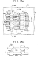
- Fig. 15A is a plan view of a planar structure of a part of the IT-CCD 10 formed on the substrate 51.
- the photodiode areas 52-1, ... , 52-i, ... serving as photocells are shaded only for ease of illustration.
- Vertical CCD channels 54-1, 54-2, ... extend between cell columns including the cell regions 52-1, ... , 52-i on the substrate 51 in parallel fashion.
- Formed on the vertical CCD channels 54-1, 54-2, ... are first transfer electrodes 56-1, 56-2, ...
- FIG. 15B A gap 60-1 extends between a convex portion 58a of the second transfer electrode 58-1 and a convex portion 56a of the first transfer electrode 56-2.
- the gap 60-1 is located at about mid-point in the width Ap of the cell column in the vertical direction.
- the remaining electrodes are also arranged in a similar fashion. In Fig. 15A, only one of the other gaps is typically illustrated using reference numeral 60-2.
- Third electrode layers 61-2, 62-2, ... are formed on the columns of the convex portion 58a, ...
- Fig. 16 shows a cross sectional view of the IT-CCD 50 taken on line XVI-XVI in Fig. 15A.
- An N + layer 64 serving as a buried channel is deposited on the top surface of the substrate 51 made of P type silicon, for example.
- a gate oxide film 66 is deposited on the N + layer 64.
- the first transfer electrodes 56-1, 56-2, ... are formed on the gate oxide film 66.
- the second transfer electrodes 58-1, 58-2, ... partially overlay the first transfer electrodes 56-1, 56-2, ... , through insulative films 66-1, 66-2, ...
- the overlaying portion of these electrodes are denoted as Ao.
- the electrode layer 62-1 is deposited.
- Three phase clock pulse voltages are applied to the first to third transfer electrodes 56, 58 and 62, respectively.
- a transfer element or a transfer unit is formed, which is composed of the first transfer electrode 56-2, the second transfer electrode 58-1, and the third transfer electrode 62-1 between the adjoining first and second transfer electrodes.
- the transfer unit corresponds to one transfer stage of the vertical CCD.
- the cross sectional structure of the IT-CCD 50 taken along line XVII-XVII in Fig. 15A has a simple structure in which the first transfer electrodes 56-1, 56-2, ... and the second transfer electrodes 58-1, 58-2, ... are laid one upon another, as shown in Fig. 17.
- the IT-CCD 50 thus arranged is simple in construction and has little deterioration of sensitivity, and is preferable for the present invention.
- FIG. 18 there is schematically shown an embodiment of an image sensor driving device (deflection device) for vibrating the Fig. 12 IT-CCD 50 in the vibration mode shown in Fig. 13.
- the IT-CCD 50 is driven to vibrate in the horizontal direction by rectangular bimorph piezoelectric elements (e.g. ceramic) of the open side type.
- a plate base (referred to as a "mother board” hereinafter) 104 has at both side edges a plurality of electrode pins 106 coupled with an external IC socket (not shown).
- a support table 108 is fixed on the mother board 100.
- the plate like bimorph piezoelectric elements 100 and 102 are fixed at one ends thereof to the support table 108 by means of adhesive, for example.
- the piezoelectric elements 100 and 102 are firmly bonded to each other, having flexible print circuited substrates (referred to as "film connectors” hereinafter) 110 and 112 sandwiched therebetween.
- the film connectors 110 and 112 electrically connect the IT-CCD 50 to the electrode pins 106 of the mother board 104.
- the image-sensed signal derived from the IT-CCD 50 is supplied to the electrode pins 106.
- the rectangular piezoelectric elements 100 and 102 are fixed to the support table 108 substantially orthogonal to the top surface of the mother board 104. Accordingly, the piezoelectric elements 100 and 102 are allowed to vibrate at the free ends thereof in the horizontal direction as indicated by an arrow 18.
- the piezoelectric elements 100 and 102 are provided at the principal surfaces with electrodes (not shown). These elements 100 and 102 are connected through the electrodes to an external circuit.
- the IT-CCD 50 is bonded to the side faces of the free ends of the pair of piezoelectric elements 100 and 102.
- the film connectors 110 and 112 are formed to substantially have a letter "Z" shape.
- Wiring patterns 113 extend along the stepped portions on the surface of the film connectors 110 and 112.
- End portions 110a and 112a of the film connectors 110 and 112 are bent in the directions of arrows 114 and 116, as shown in Fig. 18B.
- the bent end portions 110a and l12a are mounted to both sides of the IT-CCD 50 which are opposite to each other, as shown in Fig. 18A.
- the other end portions 110b and 112b of the film connectors are bent in the directions of arrows 118 and 120, as shown in Fig.
- connection area of the mother board 104 is electrically connected to the pins 106 by printed patterns (not shown) on the mother board 104.
- the image-sensed signals derived from the IT-CCD 50 are supplied to the pins 106, through the film connectors 110 and 112. The structure thus arrangeed is packed in a package (not shown).
- the image sensor deflection device thus constructed may effectively swing the IT-CCD 50 in the above-mentioned swing mode.
- the main portions of the film connectors 110 and 112, connecting the IT-CCD 50 and the pins 106 are layered and sandwiched between the pair of the piezoelectric plates 100 and 102.
- This feature prevents the vibration or swing range of the IT-CCD 50 from being limited by the film connectors 110 and 112.
- the film connectors 110 and 112 are arranged so as not to be a real load for the CCD vibration. Therefore, the IT-CCD 50 may be effectively swinged by the bimorph piezoelectric elements 100 and 102.
- Fig. 19 shows another embodiment of the invention so arranged as to vibrate or swing the IT-CCD 50 using a bimorph vibrating element of the both-end support type.
- a couple of support tables 122 and 124 are fixed in a face-to-face fashion on the top surface of the mother board 104.
- a couple of rectangular plate like bimorph piezoelectric elements 126 and 128 are fixed by the support tables 122 and 124 in a manner that their principal surfaces are faced with each other. That is, the piezoelectric plate 126 is fixed at both ends by the two support tables 122 and 124 using adhesive, for example.
- the piezoelectric plate 126 is disposed substantially normal to the mother board 104.
- the piezoelectric plate 128 is also fixedly supported at both ends by the support tables 122 and 124, and are disposed substantially in parallel with the piezoelectric plate 126. Therefore, both the piezoelectric plates 126 and 128, vibrating in the same swing mode or in a synchronized manner, serve as displacement generating elements with both ends supported.
- the piezoelectric plate 126 is made up of a couple of elemental piezoelectric plates 126-1 and 126-2. These elemental plates 126-1 and 126-2 are bonded to each other to have the film connector 130 inserted therebetween.
- the connector 130 is substantially T-shaped. Its first end portion 130a is bent to the direction of an arrow 132, and is mounted to the one of the sides of the IT-CCD 50. Second and third end portions 130b and 130c of the film connector 130 are bent to the directions of arrows 134 and 136, respectively.
- the film connector 130 is'connected at their end faces 130d and 130e to a connection area 138 formed on the top surface of the mother board 104.
- the other piezoelectric plate 128 is also constructed in a similar fashion.
- the IT-CCD 50 is bonded to the intermediate portions of the side faces of the piezoelectric plates 126 and 128. With this arrangement, the IT-CCD 50 is swinged in the horizontal direction of an arrow 18 with the vibration of the piezoelectric elements 126 and 128. Therefore, unlike the embodiment of Fig. 18, the IT-CCD 50 may exactly be swinged in the horizontal direction. Since the two piezoelectric elements 126 and 128 are used, the IT-CCD 50 is stably fixed thereon and its manufacturing is easy.
- two rectangular plate like bimorph piezoelectric elements 140 and 142 are mounted to a frame 144 fixed to the top surface of the mother board 104 through a resilient support plates 146 and 148.
- Conventional piezoelectric ceramic material of ternary system piezoelectric ceramics was used for the piezoelectric elements 140 and 142.
- the piezoelectric plates 140 and 142 were each formed by sticking together two piezoelectric ceramic plates of 5 mm in width, 18 mm in length and 0.15 mm in thickness.
- the support plates 146 and 148 are each formed by working a nickel plate of 5 mm in width and 50 ⁇ m in thickness so as to have a maximum of its displacement.
- the support plate 146 has bent portions 146a and 146b serving as spring at locations near its both ends.
- the other support plate 148 has likewise bent portions 148a and 148b.
- the piezoelectric plates 140 and 142 are fixed at the intermediate portions of the resilient support plates 146 and 148.
- the piezoelectric elements 140 and 142 thus constructed are arranged to be in parallel with each other and to vibrate in the direction of an arrow 18 together. An electric field applied to the piezoelectric elements 140 and 142 are controlled so that these plates vibrate in the same vibration mode (having the displacements and directions at a time point).
- a film connector 150 is sticked to the rear surface of the IT-CCD 50.
- the film connector 150 is made up of a main body 150-1, a pair of C-shaped legs 150-2 and 150-3 integrally connected to both ends of the main body 150-1, and a plurality of connecting portions 160 made of rubber and connected to the C-shaped legs 150-2 and 150-3.
- a necessary number of wiring patterns 162 extends following the configuration.
- the IT-CCD 50 is bonded to the side faces of the two piezoelectric plates 140 and 142, through the film connector 150.
- the C-shaped legs 150-2 and 150-3 of the film connector 150 are bent, whereby the connecting portions 160 are electrically connected, in one-to-one correspondence, to the printed patterns 164 provided on the top surface of the mother board 104 corresponding to the pins 106.
- the piezoelectric elements 140 and 142 are mounted in a floating manner to the frame 144, through support plates 146 and 148 having a spring function.
- the piezoelectric plates 140 and 142 are structured such that these are substantially floated in space, having essentially no portion fixedly coupled with other members. This unique structure of the plates remarkably increases an amount of their displacement in the vibration of the piezoelectric elements 140 and 142.
- This means that the present embodiment is well adaptable for the case to vibrate or swing a relatively heavy object (e.g. 5g) such as the IT-CCD 50.
- a relatively heavy object e.g. 5g
- a curve 170 indicate a variation of the displacement by the conventional piezoelectric element of the both-end supporting type
- a curve 172 indicates a variation of the displacement by the floating type piezoelectric elements 140 and 142 of this invention.
- a displacement corresponding to an amplitude of the drive force for swinging the IT-CCD 50 is about three times larger than that by the piezoelectric element of the both-end supporting type.
- the image sensor itself is swinged.
- the incident image light rays may be swinged against the image sensing face of the image sensor which is at a standstill.
- Fig. 22 shows a horizontal cross section of an image intensifier 180 of the electron impact type.
- photoelectrons as directed by an arrow 184 are radiated from the photosensitive face 182.
- the photoelectrons 184 are accelerated and focused by an electric field developed in the internal space of the image intensifier 180 with aid of the electrodes 186 and 188.
- the photoelectrons hit the solid state image sensor with an image sensing face 192 disposed in opposition to the photosensitive face 182 in the internal space of the image intensifier 180.
- the photoelectrons are converted into a great number of electron-hole pairs according to the known electron multiplying effect.
- the image intensifier 180 is further provided with a pair of deflection electrode plates 194 and 196.
- the electrode plates 194 and 196, provided in the image intensifier 180 are arranged oppositely each other with the photoelectron path located therebetween.
- the electrode plate 196 is grounded and the electrode 194 is electrically connected to the signal input terminal 198.
- a deflection control signal with a pulsate wave shape 200 is applied to the terminal 198.
- the voltage applied to the polarizing electrode 194 is zero.
- the field B period it is a deflection voltage V DEF .
- the photoelectrons 184 are - deflected in the horizontal direction of an arrow 202 by an amount of deflection corresponding to an intensity of the deflection field developed between the electrodes 194 and 196 by the deflection voltage V DEF applied therebetween.
- the deflection field disappears, so that the electron stream takes again the optical path as indicated by a solid line.
- This operation is repeated to substantially double the optical data collecting area of a CCD 190. Therefore, it is seen that according to the theory already described referring to Figs. 1 through 14, the incident light image may be picked up with the doubled resolution.
- the present invention which has been described using the IT-CCD, may of course be embodied using a frame transfer CCD (FT-CCD) as described in a paper bearing a title "512 x 340 Picture Elements Image Sensor" in Journal of Television Institute, pp.536 to 541, July, Vol.33, No.7.
- a common point in the image sensing operation by the solid state image sensor chip substrate between these CCD systems resides in that the signal charges stored in the photosensitive portion of each cell are simultaneously read out during the vertical blanking period. This fact implies that the solid state image sensor chip substrate, if it has the function resemble with that of these CCD systems, may be used for the present invention.
- the shape of the opening 40 was rectangular for ease of explanation.
- the IT-CCD shown in Figs. 2 and 3 employs photosensitive cells Pij, Pij' vertically arrayed in a line in each cell column, as described above.
- the photosensitive cells may be arrayed in a zig-zag fashion. The zig-zag arrayed photosensitive portions will further improve the resolution in question.
- this invention is applicable for a color television camera with one, two or three image sensors. If the combination of this invention and the picture elements swinging method as mentioned above is applied for the two- or three-plate television camera, the resolution is further improved.
- the amplitude of the vibration is shorter than the cell pitch in the aforementioned embodiments.
- the picture element pitch is longer than that of the above-mentioned case. Therefore, if the present invention is applied for the single-plate color television camera, it is preferable to extend the swing amplitude up to the distance between the adjacent cells, for lessening the moire signals produced for the color signal.
- the present invention may change the vibration amplitude so long as the high resolution is kept.
- the present invention is also applicable for a called two-stage sensor in which a photoconductive film is used for the photoelectric conversion, and the conventional silicon single crystal substrate, for example, is used for the read scanning.
- the time point of the signal charge shift from the photosensitive portions to the vertical CCDs Cl to CM is exactly coincident with the time that the vibrating the IT-CCD passes the vibration center. This time coincidence between them is not essential in the present invention, however. In contract with this, these timings may be shifted positively. If so, the increased sensitivities of the picture elements of the vibrating CCD are superposed to prevent undesirable phenomenon originating from the false signal generation, such as moire.
Abstract
Description
- The present invention relates to solid state image sensors, and more particularly to solid state image sensors for reproducing high definition images.
- Charge transfer devices (CTD) such as charge coupled devices have been known as solid state image sensors adaptable for standard television system, for example, National Television Systems Committee (NTSC) system and have found a variety of applications. In NTSC system, the number of vertical scanning lines is 512, the scanning system is of an interlacing scanning type with two fields for one frame, and the aspect ratio is 3:4. The number of picture elements of a CCD adaptable for the standard TV system, for example, in interline transfer type CCD (IT-CCD) is approximately 500 (vertical) x 400 (horizontal).
- The solid state image sensor such as the IT-CCD is superior to the conventional image pick-up tube in many points. For example, the image sensor is small in size, light in weight, and high in reliability. Further, it is essentially free from the pattern distortion and sticking, and is little influenced by afterimage sensor with such excellent features has a prospect of increasing applications in many fields, for example, ITV, small commercial video cameras which will supercede the conventional cameras using silver salt-film. For applying the image sensor for such fields, a remarkable resolution improvement of the reproduced picture is required for the solid state image sensor in order to ensure a high quality of picture.
- High definition wide television system, which can provide wide and high definition pictures are prospective television systems as the next generation television. The study of the high definition wide television system reports that the scanning lines must be 1,000 or more, for example, 1,125. To satisfy such requirement, the improvement of the resolution of the solid state image sensor is very of significance.
- The number of picture elements 500 x 400 of the currently used solid state image sensor, for example, IT-CCD, is too small to realize the high resolution. Therefore, it is considered that the number of picture elements must be remarkably increased. It is to be noted that the solid state image sensor currently used needs one of the largest chip sizes of LSIs. Therefore, if the number of picture elements is simply increased for the above purposes, the chip size of the image sensor is considerably increased. This leads to increase of the size and cost of the image sensor. On the other hand, if the number of picture elements is increased while keeping the present chip size of the image sensor, the integration density of the chip must considerably be improved, for example, four times or more. The LSI chips with such a high integration density, however, involves a difficulty in fabricating them by the fabricating technology at the present stage. Even if in the future, the fabricating technology advances and realizes the solid state image sensors with a high integration density, a new problem arises that a drive system for such image sensors must be complicated and consume large power.
- Accordingly, an object of the present invention is to provide a new and improved solid state image sensor with a high resolution.
- Another object of the present invention is to provide a new and improved solid state image sensor having a resolution comparable with that of the solid state image sensor which has successfully increased the number of picture elements without increasing the chip size or the integration density of picture elements.
- A solid state image sensor according to the present invention is provided with a solid state image sensing device such as a charge transfer device. The image sensing device includes a sensing section which receives incident radiation representing image information, generates and stores charges-corresponding to the radiation, and at least one transfer section. The sensing section is provided with at least one train of cells including a predetermined number of cells. The transfer section is disposed adjacent to and extends . along the cell train. The transfer section reads out and transfers the charges stored in the sensing section. The image sensor of the invention is further provided with a device for generating a vibration to provide a position reciprocal replacement of the cell train between the incident radiation and the image sensing device at given time periods. The vibration of the cell train is done for sensing the light image at different positions with respect to the incident radiation at different time points. With this arrangement, an effective image sensing area of the image sensing device is increased. Consequently, the resolution of the reproduced picture may be improved without increasing the integration density of the cell train. Thus, fine and definite reproduced picture may be obtained.
- The present invention is best understood by reference to the accompanying drawings, in which:
-
- Fig. 1 is a block diagram showing an overall arrangement of a solid state image sensor according to one embodiment of the present invention;
- Fig. 2 is a plan view of an image sensing area of an interline transfer charge coupled device (IT-CCD) of Fig. 1;
- Fig. 3 is a partial plan view of an area in the image sensing area of Fig. 2, which corresponds to one picture element;
- Fig. 4A illustrates a model of a vibration or swing of one picture element area in Fig. 3 for illustrating an IT-CCD swing mode in Fig. 1;
- Fig. 4B shows a waveform of vibration of IT-CCD illustrated corresponding to one picture element area in Fig. 3A;
- Fig. 5A is a waveform of an electrical signal supplied to a field shift gate (FSG) of IT-CCD in Fig. 1 during a period of one frame;
- Fig. 5B shows a waveform of swing of the IT-CCD illustrated corresponding to the signal waveform of Fig. 5A;
- Fig. 6A illustrates a model of swing of a part of the image sensing area for explaining another swing mode of the IT-CCD of Fig. 1;
- Fig. 6B is a waveform of another swing mode of the IT-CCD illustrated corresponding to the partial image sensing area of Fig. 6A;
- Fig. 7A illustrates a waveform of swing illustrating yet another swing mode of the IT-CCD;
- Fig. 7B illustrates an effective photosensint distribution of the IT-CCD vibrating in the swing mode of Fig. 7A;
- Fig. 7C shows an effective photosensing distribution of the IT-CCD vibrating in a trapezoidal wave swing mode shown in Figs. 4B and 6B;
- Fig. 8 shows a waveform illustrating a sinusoidal swing mode as a modification of the triangle swing mode of Fig. 7A;
- Fig. 9A illustrates a model of one cell area illustrating a swing mode adaptable for an image sensing or pick-up system in which one frame is composed of four fields;
- Figs. 9B and 9C show graphs illustrating X- and Y-axial displacements of the IT-CCD swinging in the swing mode of Fig. 9A with respect to time;
- Fig. 9D illustrates a waveform of an electrical signal supplied on an FSG in the IT-CCD swinging in the swing mode of Fig. 9A;
- Fig. 10A shows a model of a modification of a swing mode shown in Fig. 9A;
- Figs. 10B and 10C are graphs illustrating X- and Y-axial displacements of the IT-CCD swinging in the swing mode of Fig. 10A;
- Fig. 10D shows a graph illustrating a swing waveform in a swing mode adaptable for an image sensing system of the type in which one frame is composed of eight fields;
- Fig. 11A is a model illustrating another modification of the swing mode shown in Fig. 9A;
- Figs. 11B and 11C show graphs illustrating X- and Y-axial displacements of the IT-CCD swinging in the swing mode shown in Fig. 11A;
- Fig. 12 shows an arrangement of an IT-CCD which corresponds to the Fig. 2 IT-CCD of which the planer surface of the image sensing area is modified, with the vertical CCD having the same number of transfer stages as that of the number of picture elements of the cell line adjacent to the vertical CCD;
- Fig. 13 shows a partial plan view of the image sensing area of the IT-CCD for illustrating a displacement of a cell matrix of IT-CCD when the Fig. 12 IT-CCD is horizontally vibrated;
- Fig. 14 shows a partial plan view of the image sensing area of the IT-CCD for illustrating a displacement of the cell array for vibrating the Fig. 12 IT-CCD in a slanted direction;
- Fig. 15A is a partial plan view showing the practical structure of the IT-CCD of Fig. 12;
- Fig. 15B shows an enlarged plan view of a part of the IT-CCD for definitely illustrating electrode layers overlaid with respect to each other in Fig. 15A;
- Fig. 16 shows a partial cross sectional view taken on line XVI-XVI;
- Fig. 17 shows a partial cross sectional view illustrating a cross sectional view taken on line XVII-XVII in Fig. 15A;
- Fig. 18A is a perspective view of an image sensor deflection device for vibrating or swinging the Fig. 12 IT-CCD in the vibration mode of Fig. 13;
- Fig. 18B shows a perspective view of a structure of a plate type bimorph vibrating element fixed sandwiching the film connector of Fig. 18A;
- Fig. 19A shows a perspective view of a modification of the image sensor deflection device of Fig. 18A;
- Fig. 19B shows a perspective view of an arrangement of one of the bimorph piezoelectric elements used in the image sensor deflection device of Fig. 19A;
- Fig. 20 shows a perspective view of another modification of the image sensor deflection device of Fig. 18A;
- Fig. 21 shows a displacement characteristic of a bimorph piezoelectric element of the image sensor deflection device of Fig. 20; and
- Fig. 22 is a longitudinal cross sectional view of an image intensifier which is another embodiment of the present invention.
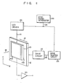
- Referring now to Fig. 1, there is schematically shown a solid state image sensor arrangement according to an embodiment of the present invention. The image sensor arrangement is so designed that a solid state image sensor per se vibrates or swings for incident light image. In Fig. 1, a solid stage image sensor, for example, an interline transfer charge coupled device (IT-CCD) 10 has an ordinary number of picture elements, for example, 500 x 400. The IT-CCD is fixed to a vibrating table 12, at the rear side 10b opposite to the image sensing area 10a. The vibrating table 12 vibrates or swings in a plane normal to the incident image rays 16, in a given direction, for example, a horizontal direction as indicated by an
arrow 18. Accordingly, the IT-CCD 10 fixed to the vibrating table 12 vibrates or swings in the vibrating mode, too. - The IT-
CCD 10 is electrically connected through agate terminal 19 to aCCD driver 20. TheCCD driver 20 responds to async pulse signal 24 generated by a syncsignal generating circuit 22, thereby to mechanically drive the IT-CCD 10. The syncsignal generating circuit 22 is also electrically connected to awave shaping circuit 26 connected to thedrive circuit 14. Thewave shaping circuit 26 receives thesync pulse signal 24 from the syncsignal generating circuit 22 and wave-shapes thesync pulse signal 24 to produce async pulse signal 28 necessary for vibrating the vibrating table 12. The wave-shapedsync pulse signal 28 is supplied to thedrive circuit 14 for vibrating the table 12. The output terminal of the vibrating or swinging IT-CCD 10 is connected to avideo signal amplifier 30. - The IT-
CCD 10 is provided with aphotosensitive portion 32 made up of photosensitive elements, for example, photodiodes Pll, Pll', P12, P12', ... , PIN, PIN', ... , Pij, Pij', ... , PMN, PMN'. Of photodiodes P vertically arranged, the adjacent photodiodes are paired and designated by paired notation, as just above. This is done for making the notation of the photodiodes arrayed comply with the conventional one adaptable for NTSC system. These photodiodes P are arrayed on a CCD substrate (not shown) in a matrix fashion. In the matrix array each column includes photodiodes of 2N and the columns of M are arrayed side by side. M vertical CCDs Cl to CM are disposed adjacent to the M photodiodes columns, respectively. The number of vertical CCDs C1 to CM is equal to the number of vertical picture elements in the IT-CCD 10, that is, the half (N) of the number of photodiodes contained in each photodiode column. The vertical CCDs C1 to CM are connected at their final transfer stage to a horizontal CCD shift register S. A field shift gate (FSG) 34 is arranged with the gate portions each extending through gaps between the vertical photodiode columns P1 to PM and the vertical CCDs Cl to CM. The.FSG 34 is electrically connected to thegate terminal 19. When a pulse signal (a gate control signal) is applied from theCCD driver 20 to theFSG 34 through thegate terminal 19, the signal charge stored in the photodiodes P is transferred to the vertical CCDs Cl to CM. The signal charge transferred to the vertical CCDs Cl to CM is sequentially transferred to the horizontal CCD shift register S for each stage. The charge is then read out from theoutput terminal 36 through theamplifier 30. - Fig. 3 shows an enlarged plan view of an image sensing area corresponding to one picture element or one cell in the
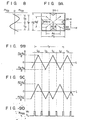
photosensitive portion 32 of the IT-CCD 10 in Fig. 2. A hatchedportion 38 indicates an aluminum electrode serving to shut off the incident light. TheAt electrode 38 has anopening 40 under which the photodiode Pij' is located. The vertical CCD Ci and theFSG 34 run under theAt electrode 38, and hence are optically shielded from light rays by theAt electrode 38. An internal interconnection pattern (not shown) for driving the vertical CCD Ci is formed under anarea 42 of theAt electrode 38 located above the photodiode Pij. Thearea 42 of theAℓ electrode 38 performs optical isolation between the photodiodes Pij and Pij'. - The present embodiment is applied for the image sensing based on NTSC television system. Accordingly, the IT-
CCD 10 is vibrated or swinged horizontally in Fig. 1, i.e. in the horizontal direction, at a period corresponding to one frame period tF (two fields period) in the image sensing operation. The vibration mode (or swing mode) of the IT-CCD 10 will now be described referring to Figs. 4 and 5. - Fig. 4A illustrates again the one cell area shown in Fig. 3 in a model, for explaining the swing mode of the IT-
CCD 10. The IT-CCD 10 is swinged, according to a vibration waveform as shown in Fig. 4B, so that during a field A in one frame period tF, theopening 40 where the one cell Pij' of the IT-CCD 10 is located at a first location as indicated by a solid line in Fig. 4A, on the other hand, during a field B, it is positioned at a second location denoted by a dottedline 44. The swing width of the CCD is denoted as A. If the center of the swing in this coordinates system is 0, the CCD reciprocately swings a A/2 distance positively and negatively with respect to the center 0. If the period ts (Fig. 4B) that the center 40c of theopening 40 of theAℓ electrode 38 moves from X = A/2 to -X = A/2 is sufficiently shorter than the one frame period tF, the opening center 40c, i.e. the center of the cell Pij', rests at X = A/2 during the field A period ta. During the field B period tb, it rests at X = -A/2. Since the amplitude A is set much smaller than the horizontal pitch length PH, the cell has substantially two different spatial sampling areas in the horizontal direction during the one frame period tF. While one cell Pij have typically been described, the same thing is true for the remaining cells. - In Fig. 5, there are shown a voltage signal waveform φFSG from the photosensitive portion to the
FSG 34 for controlling the transfer of the signal charge to the vertical CCDs C1 to CM, and a time variation φA of the opening center 40c. As shown in Fig. 5A, the voltage signal from theCCD driver 20 in a pulse signal changing between a low level potential VL and a high level potential VH. During the vertical blanking period tVB of the IT-CCD 10, the pulse component at high level potential VH is applied to the FSG 34 (Fig. 2). The signal charge stored in thephotosensitive section 32 by image-sensing the incident image light rays is transferred through theFSG 34 to the vertical CCDs C1 to CM. The time variation waveform φA of position of the cell center 40c shown in Fig.. 5B is so arranged as to cross the coordinate X = 0 during the vertical blanking period tVB and within a period that the pulse signal from theCCD driver 20 shown in Fig. 5A is at VH. Accordingly, the signal charge stored in thephotosensitive section 32 during the field A period ta corresponds to the image light incident on the IT-CCD 10 when the IT-CCD 10 is positioned at X = A/2. The signal charge obtained during the field B period tb corresponds to the image light incident on the IT-CCD 10 when the IT-CCD 10 is at X = -A/2. - The IT-
CCD 10 thus arranged according to the present invention, unlike the conventional IT-CCD picking up an image at the same position through the periods of fields A and B, may pick up an image from the incident image light at different positions during the periods of fields A and B. In reproducing the image thus formed, if the read out cell signals or the image picture signals of the fields A and B thus obtained are visualized spacially shifted in horizontal direction so as to be adapted for the aforementioned CCD sampling operation, the resolution of the reproduced picture can be improved essentially two times. In the present embodiment, the cell center 40c merely reciprocates in horizontal direction every field period. The horizontal reciprocal movement of the IT-CCD 10 has little adverse influence on the vertical resolution of the reproduced picture. - As described above, the present embodiment employs the solid state image sensor such as IT-CCD arranged such that the signal charge stored in the photosensitive section are simultaneously read out and transferred to the vertical CCD sections for each field and during the blanking period. The image sensor is vibrated or swinged in a vertical plane with respect to the incident image light. In more particular, during the periods of the fields A and B, the image-sensor stops at two different positions. And during the blanking period,. the image sensor reciprocately and radially moves between two different positions. With such an arrangement, the effective horizontal resolution may be doubled without deteriorating the vertical resolution, thus providing a fine and high quality picture reproduced.
- Even if the fabrication technique in this field will further be increased and this technique may realize a solid state image sensor of which the picture elements are packed in density two times in horizontal direction, it should be noted that the image sensor of the present invention is advantageous over such image sensor with high integration density and has the following advantages.
- (1) In the image sensor with highly density integration, the cell pitch is halved. Therefore, the saturation signal level is remarkably reduced to cause the dynamic range to be excessively narrower. On the other hand, the image sensor according to the present invention is free from such problem about the dynamic range characteristic. Further, it can excellently remove the deterioration of the picture quality (such as smear-or blooming) which arises from the diffusion of the signal charge in the substrate when the integration density is increased and hence the distance between the photosensitive portion and the vertical CCD is made small. Thus, according to the present invention, the solid state image sensor with a wide dynamic range can be provided without using special and so high fabrication technique.
- (2) On the image sensor with high integration density, the read speed of the cell signal (image-sensed signal) is substantially doubled. Many problems undesirably arises from this: for example, increase of power consumption and difficulty in circuit design on the circuits for driving the highly packed image sensor and the peripheral circuits for signal processing. The image sensor of the present invention is free from such problems.
- (3) In the image sensor with high integration density, a ratio of each cell area to the substrate area is of necessity small. Accordingly, ratio of the opening area in each cell to the substrate area is also small and is never large. It can not be expected accordingly that the increase of the integration density brings about decrease of the ineffective area in the photosensitive area of such image sensor in collecting light image information. On the other hand, the image sensor according to the present invention can substantially collect the light image data from the area corresponding to the actual ineffective area by the vibration of the image sensor per se. Thus, the image sensor of the present invention has an effectively wide area for collecting the optical image information.
- As described above, how to set up a relationship between the time variation of position φA of the chip substrate of the swinging solid state image sensor and the signal charge read out operation, is one of the most important factor in realizing the high resolution of the reproduced picture.
- Fig. 6 shows a modification of the swing mode of the aforementioned embodiment. In this swing mode, the opening center 40c in one cell area horizontally swings a distance of
P H/4 from its swing center in the positive and negative directions. The other fundamental swinging operations are similar to those in the above embodiment. The waveform on the graph of Fig. 6B, which represents a vibration of IT-CCD, is a trapezoidal waveshape. - A model of the image sensing cells reciprocatingly moving rest at two different positions during both fields A and B when the IT-
CCD 10 is vibrated or swinged, is illustrated in Fig. '6A. The cell array as a model in Fig. 6A is illustrated for each frame period. In Fig. 6A, cell positions, as indicated by a solid line during a field A period and as indicated by a dotted line during a field B period, are arranged so as to be distanced by equal pitch length PH/2 from one another. If the IT-CCD 10 is swinged under this cell array condition, it is possible to prevent generation of moire signal. Therefore, the resolution of the reproduced picture may further be improved. - Turning now to Fig. 7, there is shown still another modification of swing mode of the embodiments shown in Figs. 1 to 5. According to a "triangle swing mode" the IT-CCD horizontally swings with an amplitude PH-PA, where AH is a length of opening as horizontally viewed. In the present instance, the swing center of the IT-CCD is just positioned at the coordinate X = 0 during the vertical blanking period, as in the previous instances. When such "triangle vibration mode" is used, the effective photosensitive cell area is uniformly and continuously expanded within a swing amplitude distance over an entire area of one frame period tF consisting of two periods of fields A and B, as shown in Fig. 7B. In Fig. 7B, symbol "e" indicates a sensitivity. This arises from the fact that, during one frame period tF, the IT-CCD senses the light image while always moving without the rest of the
opening 40. In this instance, therefore, the ineffective area for the image sensing (the area is ineffective in photosensing or image sensing) may be remarkably reduced. When the called "trapezoidal swing mode" already referred to Figs. 4B and 6B is used, extremely low sensitivity areas denoted as 48 are necessarily present. Accordingly, undesirable moire signal tends to generate. Particularly, when the IT-CCD having a cell opening with a small horizontal length AH is used, the adverse influence by the false signals is serious. When the "triangle wave swing mode" shown in Fig. 7A is used, however, this problem may easily be solved. - In Fig. 8, there is shown a "sinusoidal wave swing mode", which may be considered as a compromise of the "trapezoidal wave swing mode" and the "triangle wave swing mode". In this instance, the amplitude is PH. This instance may effect the image sensing with small ineffective area.
- While having been described using the embodiment applied for the NTSC television-system, the present invention is not limited by such instances in any way. In image pick-up systems other than the television system, for example, electronic camera (still camera) not using the silver salt-film and OCR, both being a closed system, the scanning system is not limited by the two-field for one frame. Therefore, if the present invention is applied for such image pick-up system, the resolution is further improved.
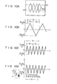
- Fig. 9 shows a modification of the above-mentioned vibration mode when the present invention is applied for the image pick-up system of the multi-field for one frame type. In this instance, four fields A, B, C and D make up one frame. The IT-
CCD 10 is vibrated radially in four directions about the vibration center 0, corresponding to four field periods, as shown in Fig. 9A. In Fig. 9A, the amplitudes of the X- and Y-axial swing components in the swing mode of this instance are, respectively, PG - AG and PG' - AG', where AG is the horizontal (X-axial) width of the cell area and AG', the vertical (Y-axial) width. The vibration mode components in the respective directions are shown in Figs. 9B and 9C. - By using such vibration mode, four effective image sensing picture elements may be obtained for one real cell during one frame period. A waveform φFSG of the pulse signal or gate control signal applied to FSG 34 (Fig. 1), and a time variation of vibration of the IT-CCD are timed as shown in Fig. 9D, and substantially the same as in Fig. 5. When the gate control signal FSG is at high voltage level Vg, the IT-
CCD 10 is positioned at the vibration center 0. A resolution of the reproduced picture is substantially four times that of the conventional IT-CCD which is not swinged for image sensing. In Fig. 9A, ineffective portions 50-1, 50-2, 50-3 and 50-4, which are hatched in illustration, are present. Theineffective portion 50 may easily be improved by a skilled person in the art. For example, all one it may be improved by increasing the area of the openingportion 40. - Fig. 10 shows an embodiment of the present invention which is arranged to reduce the ineffective area in the cell of the swinging IT-CCD. As shown in Fig. 10A, the IT-
CCD 10 is swinged iri a manner that the opening center 40c moves along zig-zag locus so as to have the horizontal swing component and the vertical swing component as well. By using this swing mode, the ineffective area is further decreased. In this case, the swing mode as shown in Fig. 10B is employed for the horizontal swing mode, and is same as that of Fig. 7. The swinging frequency of the vertical component is selected higher than that of the horizontal components, as shown in Fig. 10C. In Fig. 10C, PV is a vertical pitch length of one cell, and AV is a vertical length of theopening 40. - Incidentally, in a closed system, the gate control signal with a waveform φFSG like that of the above case is applied to the
FSG 34 to read out the signal charge stored in the photosensitive section 32 (Fig. 1) and transfer it to the vertical CCDs C1 to CM, when the vibration center of the vertical swing component is positioned at Y = 0, as shown in Fig. 10D. Such an arrangement enables one frame to have many fields, for example, 8 fields. In this case, as seen from Fig. 10A, the image-sensed signals obtained from the fields are overlapped one another. Nevertheless, different eight photosensing areas may be obtained from one real photosensitive cell area during one frame period. Therefore, the resolution of the reproduced picture is considerably improved. - In Fig. ll, the
opening 40 is swinged in "8" shape (Fig. 11A) in a plane normal to the incident image light. In the embodiment of Fig. 9, the horizontal or X-axial vibration component may be the called "triangle swing mode" shown in Fig. 9B. The waveform of the Y-axial swing component is a complicated "triangle waveform" as it is returned during the field C period. In the swing mode of Fig. 11A, the swing waveforms in the X- and Y-axial directions are simple sinusoidal waveforms, as shown in Figs. 11B and 11C. Therefore, the swing control of the IT-CCD is simplified. - Fig. 12 shows a solid state image sensor including an IT-
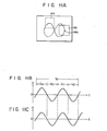
CCD 50 which is another embodiment of the present invention. The IT-CCD 50 is adaptable for the NTSC system. In Fig. 12, like reference numerals are used for designating like or equivalent portions in Fig. 1. The solid state image sensor is composed of a matrix array of photodiodes or picture element cells P of 2N x M (N = 250 and M = 400). The cell matrix includes columns of the cells P1 to PM. Each cell column contains picture element cells of 2N Pll, P11', ... , P1N, P1N', ... , PMN, PMN'. The vertical CCDs C1 to CM of M are arranged in opposition to the cell columns P1 to PM, with theFSG 34 interposing therebetween. The vertical CCDs C1 to CM have the same number of transfer stages as the picture elements contained in the cell columns P1 to PM. The first vertical CCD column C1 includes transfer elements of 2N C11, C11', ... , C1N, C1N'. The same thing is true for the remaining vertical CCD columns. The signal charges stored in the photocells Pll, Pll', ... , PlN, P1N' in each photocell columns Pl to PM are respectively and independently transferred to the transfer elements C11, C11', ... , C1N, C1N, in opposition to the vertical CCDs C1 to CM through theFSG 34, during the horizontal effective period. The signal charges loaded into the vertical CCDs C1 to CM are successively transferred to every unit of transfer elements of which the number is the same as that of the photocells included in each vertical cell columns. In the horizontal effective period, the charges are further transferred in a horizontal shift register S, and then produced through theamplifier 30 and theoutput terminal 36 in successive order. - The IT-
CCD 50 of Fig. 12 horizontally vibrates or swings in a plane normal to the incident image light and relative to the incident image light, according to the called "trapezoidal wave swing mode". The technique of vibrating the IT-CCD has already been described and hence no further explanation thereof will be given here. - Fig. 13 shows a model of a moving state of the photosensitive section in the horizontal direction when the IT-
CCD 50 of Fig. 12 swings in the "trapezoidal wave vibration mode". The amplitude of the vibration is 1/2 of the horizontal picture element pitch. In Fig. 13, during the field A in one frame period, the IT-CCD 50 just rests at a first image sensing position as indicated by a solid line. At the first image sensing position, it senses the incident light image. During the field B period, it rests at the second image sensing position as indicated by a dotted line in Fig. 13. The movement of the signal charges stored in the photocells to the vertical CCDs during each field period, is performed during a period corresponding to the vertical blanking period in the scanning operation at the picture reproducing stage, for executing an effective image sensing operation. Accordingly, during the fields A and B of one frame period, the image information may be obtained at first and second image-sensing positions which are shifted 1/2 pitch of the picture element from one another. Therefore, the present embodiment may attain a high horizontal resolution with the photocells 2N x M, or 500, and the horizontal resolution is comparable with that of the high density CCD with 1,000 picture element cells. According to the present embodiment, the signal charges stored in the photocells are independently transferred to the corresponding transfer elements of the vertical CCD, respectively. Therefore, it is prevented that the signal charges from the picture elements adjacent to each other as viewed vertically are mixed when the signal charges are transferred in the vertical CCD. This feature is useful in improving the picture quality or the resolution of the reproduced picture. - Fig. 14 shows an embodiment of the invention which may improve the horizontal resolution and the vertical resolution using a modification of the swing mode shown in Fig. 13. In Fig. 14, the IT-
CCD 50 vibrates or swings in a slanted direction denoted asreference numeral 52. Also in this case, the X- and Y-axial swing components have the "trapezoidal wave vibration mode", for example. The X-axial swing component has an amplitude of the half of the photocell pitch length Ax as horizontally viewed. The Y-axial vibration component has an amplitude of the half of the cell pitch Ay as vertically viewed. The movement of the photocell Pij of the IT-CCD 50 vibrating in such vibration mode is indicated by anarrow 54. During the field A period, each of picture element cells rests at a first image sensing position as indicated by a solid line in Fig. 14 and the image sensing is thus performed at this position. During the field B period, the cells stop and rest at a second image sensing position as indicated by a dotted line, which is different from the first image sensing position in the Fig. 13 embodiment. During this period, the image sensing is performed at this position. This operation is repeated every frame period. - For reproducing the image signal obtained according to the present image sensing system, the field image read out in synchronism with the read out clock in the fields A and B may easily provide a normal reproduced picture by vertically shifting them by the 1/2 picture element period. According to this image sensing system, as shown in Fig. 14, the field image signal components (N-1)HA, NHA, (N+1)HA, (N+2)HA, (N+3)HA, ... are read out in the field A period. In the field B period, the field picture signal components (N-l)HB, NHB, (N+1)HB, (N+2)HB, (N+3)HBi ... are read out. Therefore, the interlacing image sensing is performed not only in the horizontal direction but also in the vertical direction, corresponding to the interlacing scanning in the picture display. Almost ideal interlacing image sensing is possible, accordingly. Thus, a high vertical resolution comparable with that as given by 1,000 vertical scanning lines can be attained. Further, the horizontal resolution may be improved doubly.
- A practical arrangement of the IT-
CCD 50, which is well adaptable for the two embodiments shown in Figs. 12 to 14, will be described referring to Figs. 15 to 17. Fig. 15A is a plan view of a planar structure of a part of the IT-CCD 10 formed on thesubstrate 51. In the figure, the photodiode areas 52-1, ... , 52-i, ... serving as photocells are shaded only for ease of illustration. Vertical CCD channels 54-1, 54-2, ... extend between cell columns including the cell regions 52-1, ... , 52-i on thesubstrate 51 in parallel fashion. Formed on the vertical CCD channels 54-1, 54-2, ... are first transfer electrodes 56-1, 56-2, ... forming a first layer, which extend normal to the CCD channels 54-1, 54-2, ... Second transfer electrodes 58-1, 58-2, ... forming a second layer are further formed on the first transfer electrodes 56-1, 56-2, ... The planar structure of the first and second transfer electrodes 56 and 58 are clearly illustrated in an enlarged manner in Fig. 15B. A gap 60-1 extends between a convex portion 58a of the second transfer electrode 58-1 and a convex portion 56a of the first transfer electrode 56-2. The gap 60-1 is located at about mid-point in the width Ap of the cell column in the vertical direction. The remaining electrodes are also arranged in a similar fashion. In Fig. 15A, only one of the other gaps is typically illustrated using reference numeral 60-2. Third electrode layers 61-2, 62-2, ... are formed on the columns of the convex portion 58a, ... - Fig. 16 shows a cross sectional view of the IT-
CCD 50 taken on line XVI-XVI in Fig. 15A. An N+ layer 64 serving as a buried channel is deposited on the top surface of thesubstrate 51 made of P type silicon, for example. Agate oxide film 66 is deposited on the N+ layer 64. The first transfer electrodes 56-1, 56-2, ... are formed on thegate oxide film 66. The second transfer electrodes 58-1, 58-2, ... partially overlay the first transfer electrodes 56-1, 56-2, ... , through insulative films 66-1, 66-2, ... The overlaying portion of these electrodes are denoted as Ao. After insulative films 68-l, 68-2, ... are formed on the structure, the electrode layer 62-1 is deposited. - Three phase clock pulse voltages are applied to the first to third transfer electrodes 56, 58 and 62, respectively. With the application of the pulse voltages, a transfer element or a transfer unit is formed, which is composed of the first transfer electrode 56-2, the second transfer electrode 58-1, and the third transfer electrode 62-1 between the adjoining first and second transfer electrodes. The transfer unit corresponds to one transfer stage of the vertical CCD. The cross sectional structure of the IT-
CCD 50 taken along line XVII-XVII in Fig. 15A, has a simple structure in which the first transfer electrodes 56-1, 56-2, ... and the second transfer electrodes 58-1, 58-2, ... are laid one upon another, as shown in Fig. 17. The IT-CCD 50 thus arranged is simple in construction and has little deterioration of sensitivity, and is preferable for the present invention. - In Fig. 18, there is schematically shown an embodiment of an image sensor driving device (deflection device) for vibrating the Fig. 12 IT-
CCD 50 in the vibration mode shown in Fig. 13. The IT-CCD 50 is driven to vibrate in the horizontal direction by rectangular bimorph piezoelectric elements (e.g. ceramic) of the open side type. - In Fig. 18A, a plate base (referred to as a "mother board" hereinafter) 104 has at both side edges a plurality of electrode pins 106 coupled with an external IC socket (not shown). A support table 108 is fixed on the
mother board 100. The plate like bimorphpiezoelectric elements piezoelectric elements film connectors CCD 50 to the electrode pins 106 of themother board 104. With this connection, the image-sensed signal derived from the IT-CCD 50 is supplied to the electrode pins 106. The rectangularpiezoelectric elements mother board 104. Accordingly, thepiezoelectric elements arrow 18. Thepiezoelectric elements elements - The IT-
CCD 50 is bonded to the side faces of the free ends of the pair ofpiezoelectric elements film connectors Wiring patterns 113 extend along the stepped portions on the surface of thefilm connectors film connectors arrows CCD 50 which are opposite to each other, as shown in Fig. 18A. Theother end portions 110b and 112b of the film connectors are bent in the directions ofarrows 118 and 120, as shown in Fig. 18B, and are connected to the connection area of themother board 104, as shown in Fig. 18A. The connection area of themother board 104 is electrically connected to thepins 106 by printed patterns (not shown) on themother board 104. With this arrangement, the image-sensed signals derived from the IT-CCD 50 are supplied to thepins 106, through thefilm connectors - The image sensor deflection device thus constructed may effectively swing the IT-
CCD 50 in the above-mentioned swing mode. As described above, the main portions of thefilm connectors CCD 50 and thepins 106, are layered and sandwiched between the pair of thepiezoelectric plates CCD 50 from being limited by thefilm connectors film connectors CCD 50 may be effectively swinged by the bimorphpiezoelectric elements - Fig. 19 shows another embodiment of the invention so arranged as to vibrate or swing the IT-
CCD 50 using a bimorph vibrating element of the both-end support type. A couple of support tables 122 and 124 are fixed in a face-to-face fashion on the top surface of themother board 104. A couple of rectangular plate like bimorphpiezoelectric elements piezoelectric plate 126 is fixed at both ends by the two support tables 122 and 124 using adhesive, for example. Thepiezoelectric plate 126 is disposed substantially normal to themother board 104. Thepiezoelectric plate 128 is also fixedly supported at both ends by the support tables 122 and 124, and are disposed substantially in parallel with thepiezoelectric plate 126. Therefore, both thepiezoelectric plates - The
piezoelectric plate 126 is made up of a couple of elemental piezoelectric plates 126-1 and 126-2. These elemental plates 126-1 and 126-2 are bonded to each other to have thefilm connector 130 inserted therebetween. Theconnector 130 is substantially T-shaped. Its first end portion 130a is bent to the direction of anarrow 132, and is mounted to the one of the sides of the IT-CCD 50. Second andthird end portions 130b and 130c of thefilm connector 130 are bent to the directions ofarrows film connector 130 is'connected at their end faces 130d and 130e to aconnection area 138 formed on the top surface of themother board 104. The otherpiezoelectric plate 128 is also constructed in a similar fashion. - The IT-
CCD 50 is bonded to the intermediate portions of the side faces of thepiezoelectric plates CCD 50 is swinged in the horizontal direction of anarrow 18 with the vibration of thepiezoelectric elements CCD 50 may exactly be swinged in the horizontal direction. Since the twopiezoelectric elements CCD 50 is stably fixed thereon and its manufacturing is easy. - In an embodiment of Fig. 20, two rectangular plate like bimorph
piezoelectric elements frame 144 fixed to the top surface of themother board 104 through aresilient support plates piezoelectric elements piezoelectric plates support plates support plate 146 has bentportions 146a and 146b serving as spring at locations near its both ends. Theother support plate 148 has likewise bentportions 148a and 148b. Thepiezoelectric plates resilient support plates piezoelectric elements arrow 18 together. An electric field applied to thepiezoelectric elements - A
film connector 150 is sticked to the rear surface of the IT-CCD 50. Thefilm connector 150 is made up of a main body 150-1, a pair of C-shaped legs 150-2 and 150-3 integrally connected to both ends of the main body 150-1, and a plurality of connectingportions 160 made of rubber and connected to the C-shaped legs 150-2 and 150-3. In the legs 150-2 and 150-3, a necessary number ofwiring patterns 162 extends following the configuration. The IT-CCD 50 is bonded to the side faces of the twopiezoelectric plates film connector 150. At this time, the C-shaped legs 150-2 and 150-3 of thefilm connector 150 are bent, whereby the connectingportions 160 are electrically connected, in one-to-one correspondence, to the printedpatterns 164 provided on the top surface of themother board 104 corresponding to thepins 106. - According to the embodiment of Fig. 20, the
piezoelectric elements frame 144, throughsupport plates piezoelectric plates piezoelectric elements CCD 50. Fig. 21 illustrates a graph of experimental data displacements given by the conventional bimorph piezoelectric element of the both-end supporting type and by the bimorph piezoelectric element of the open-end type of this invention with respect to the applied voltage. In the figure, acurve 170 indicate a variation of the displacement by the conventional piezoelectric element of the both-end supporting type, and acurve 172 indicates a variation of the displacement by the floating typepiezoelectric elements CCD 50 is about three times larger than that by the piezoelectric element of the both-end supporting type. - Although the present invention has been shown and described with respect to particular embodiments, nevertheless, various changes and modifications which are obvious to a person skilled in the art to which the invention pertains are deemed to lie within the spirit, scope, and contemplation of the invention.
- In the above-described embodiments, in order to attain a relative swing between the incident image light rays and the solid state image sensor such as the IT-CCD, the image sensor itself is swinged. It should be understood that the present invention is not limited by such embodiments. For example, the incident image light rays may be swinged against the image sensing face of the image sensor which is at a standstill.
- This instance will be described in detail referring to Fig. 22. Fig. 22 shows a horizontal cross section of an
image intensifier 180 of the electron impact type. When theimage light 181 is incident on the photosensitive face, photoelectrons as directed by anarrow 184 are radiated from thephotosensitive face 182. Thephotoelectrons 184 are accelerated and focused by an electric field developed in the internal space of theimage intensifier 180 with aid of theelectrodes image sensing face 192 disposed in opposition to thephotosensitive face 182 in the internal space of theimage intensifier 180. The photoelectrons are converted into a great number of electron-hole pairs according to the known electron multiplying effect. Theimage intensifier 180 is further provided with a pair ofdeflection electrode plates electrode plates image intensifier 180, are arranged oppositely each other with the photoelectron path located therebetween. - Of these electrodes, the
electrode plate 196 is grounded and theelectrode 194 is electrically connected to thesignal input terminal 198. When this embodiment is used in NTSC television system, a deflection control signal with apulsate wave shape 200 is applied to the terminal 198. In a field A period, the voltage applied to thepolarizing electrode 194 is zero. In the field B period, it is a deflection voltage VDEF. Accordingly, when the field period is shifted from the field A period to the field B period, thephotoelectrons 184 are - deflected in the horizontal direction of anarrow 202 by an amount of deflection corresponding to an intensity of the deflection field developed between theelectrodes CCD 190. Therefore, it is seen that according to the theory already described referring to Figs. 1 through 14, the incident light image may be picked up with the doubled resolution. - The present invention, which has been described using the IT-CCD, may of course be embodied using a frame transfer CCD (FT-CCD) as described in a paper bearing a title "512 x 340 Picture Elements Image Sensor" in Journal of Television Institute, pp.536 to 541, July, Vol.33, No.7. A common point in the image sensing operation by the solid state image sensor chip substrate between these CCD systems resides in that the signal charges stored in the photosensitive portion of each cell are simultaneously read out during the vertical blanking period. This fact implies that the solid state image sensor chip substrate, if it has the function resemble with that of these CCD systems, may be used for the present invention. In the above-mentioned embodiments, the shape of the
opening 40 was rectangular for ease of explanation. If the opening has other shapes, the number of the sampling points are not decreased. Such shapes may of course be involved in this invention. The IT-CCD shown in Figs. 2 and 3 employs photosensitive cells Pij, Pij' vertically arrayed in a line in each cell column, as described above. The photosensitive cells may be arrayed in a zig-zag fashion. The zig-zag arrayed photosensitive portions will further improve the resolution in question. - It is evident that this invention is applicable for a color television camera with one, two or three image sensors. If the combination of this invention and the picture elements swinging method as mentioned above is applied for the two- or three-plate television camera, the resolution is further improved.
- The amplitude of the vibration is shorter than the cell pitch in the aforementioned embodiments. In the single-plate color television camera, the picture element pitch is longer than that of the above-mentioned case. Therefore, if the present invention is applied for the single-plate color television camera, it is preferable to extend the swing amplitude up to the distance between the adjacent cells, for lessening the moire signals produced for the color signal. The present invention may change the vibration amplitude so long as the high resolution is kept.
- The present invention-is also applicable for a called two-stage sensor in which a photoconductive film is used for the photoelectric conversion, and the conventional silicon single crystal substrate, for example, is used for the read scanning.
- In the Figs. 4 to 11 embodiments, the time point of the signal charge shift from the photosensitive portions to the vertical CCDs Cl to CM is exactly coincident with the time that the vibrating the IT-CCD passes the vibration center. This time coincidence between them is not essential in the present invention, however. In contract with this, these timings may be shifted positively. If so, the increased sensitivities of the picture elements of the vibrating CCD are superposed to prevent undesirable phenomenon originating from the false signal generation, such as moire.
Claims (20)
Applications Claiming Priority (8)
| Application Number | Priority Date | Filing Date | Title |
|---|---|---|---|
| JP56209381A JPS58111580A (en) | 1981-12-25 | 1981-12-25 | Solid-state image pickup device |
| JP209381/81 | 1981-12-25 | ||
| JP57039429A JPS58157263A (en) | 1982-03-15 | 1982-03-15 | Image pickup system of solid-state image pickup device |
| JP39429/82 | 1982-03-15 | ||
| JP57078331A JPS58196775A (en) | 1982-05-12 | 1982-05-12 | Deflecting device of solid-state image pickup element |
| JP57078328A JPS58196773A (en) | 1982-05-12 | 1982-05-12 | Deflecting device of solid-state image pickup element |
| JP78328/82 | 1982-05-12 | ||
| JP78331/82 | 1982-05-12 |
Publications (3)
| Publication Number | Publication Date |
|---|---|
| EP0083240A2 true EP0083240A2 (en) | 1983-07-06 |
| EP0083240A3 EP0083240A3 (en) | 1984-09-12 |
| EP0083240B1 EP0083240B1 (en) | 1988-06-01 |
Family
ID=27460758
Family Applications (1)
| Application Number | Title | Priority Date | Filing Date |
|---|---|---|---|
| EP82306971A Expired EP0083240B1 (en) | 1981-12-25 | 1982-12-24 | Solid state image sensor with high resolution |
Country Status (2)
| Country | Link |
|---|---|
| EP (1) | EP0083240B1 (en) |
| DE (1) | DE3278604D1 (en) |
Cited By (15)
| Publication number | Priority date | Publication date | Assignee | Title |
|---|---|---|---|---|
| EP0150973A2 (en) * | 1984-01-31 | 1985-08-07 | Kabushiki Kaisha Toshiba | Wobbling-swing driven image sensor |
| EP0161752A2 (en) * | 1984-04-13 | 1985-11-21 | Kabushiki Kaisha Toshiba | Image signal reproduction circuit for swing image sensor |
| GB2172168A (en) * | 1985-03-09 | 1986-09-10 | English Electric Valve Co Ltd | Camera tilt/pan mechanisms |
| GB2204210A (en) * | 1987-04-27 | 1988-11-02 | Marconi Gec Ltd | Imaging system |
| EP0395913A2 (en) * | 1989-05-03 | 1990-11-07 | Robert Bosch Gmbh | Image pickup device |
| US4975779A (en) * | 1985-12-06 | 1990-12-04 | The Computer Film Company Limited | Method of recording an image |
| EP0490246A1 (en) * | 1990-12-11 | 1992-06-17 | Sony Corporation | Solid-state imager |
| EP0506188A1 (en) * | 1991-03-29 | 1992-09-30 | Koninklijke Philips Electronics N.V. | Charge-coupled device |
| WO1992022092A1 (en) * | 1991-06-07 | 1992-12-10 | Eastman Kodak Company | Ccd electrode structure for image sensors |
| DE4223693A1 (en) * | 1992-07-21 | 1994-01-27 | Siemens Ag | X=ray image intensifier e.g. for medical diagnosis - has image sensor comprising layer system with semiconductor layer of amorphous semiconductor material for electron conversion |
| US5349178A (en) * | 1992-06-22 | 1994-09-20 | Siemens Aktiengesellschaft | Image intensifier with protected image sensor |
| EP0697786A1 (en) * | 1994-08-16 | 1996-02-21 | Matra Marconi Space France | Device for earth sensing for satellite or similar having an array of pyroelectrical detectors |
| WO2000041034A1 (en) * | 1998-12-31 | 2000-07-13 | Metis Systems, S.R.L. | High-resolution photographic apparatus, in particular for wide dimensioned objects |
| DE10033751B4 (en) * | 2000-07-12 | 2004-09-16 | Lenz, Reimar, Dr. | Digital, high-resolution cinema film camera |
| EP1931133A1 (en) | 2006-12-07 | 2008-06-11 | Sick Ag | Method and device for optical acquisition of a structure |
Citations (3)
| Publication number | Priority date | Publication date | Assignee | Title |
|---|---|---|---|---|
| FR2486387A1 (en) * | 1980-07-11 | 1982-01-15 | Siemens Ag | RADIODIAGNOSTIC INSTALLATION WITH SOLID STATE IMAGE CONVERTER |
| EP0065885A1 (en) * | 1981-03-27 | 1982-12-01 | Thomson-Csf | Device for producing television pictures with a charge-transfer matrix |
| EP0067043A2 (en) * | 1981-06-10 | 1982-12-15 | Kabushiki Kaisha Toshiba | Solid-state color television camera device |
-
1982
- 1982-12-24 DE DE8282306971T patent/DE3278604D1/en not_active Expired
- 1982-12-24 EP EP82306971A patent/EP0083240B1/en not_active Expired
Patent Citations (3)
| Publication number | Priority date | Publication date | Assignee | Title |
|---|---|---|---|---|
| FR2486387A1 (en) * | 1980-07-11 | 1982-01-15 | Siemens Ag | RADIODIAGNOSTIC INSTALLATION WITH SOLID STATE IMAGE CONVERTER |
| EP0065885A1 (en) * | 1981-03-27 | 1982-12-01 | Thomson-Csf | Device for producing television pictures with a charge-transfer matrix |
| EP0067043A2 (en) * | 1981-06-10 | 1982-12-15 | Kabushiki Kaisha Toshiba | Solid-state color television camera device |
Non-Patent Citations (1)
| Title |
|---|
| IEEE TRANSACTIONS ON ELECTRON DEVICES, vol. ED-20, no. 6, June 1973, pages 535-541, New York, US C.H. SEQUIN: "Interlacing in charge-coupled imaging devices" * |
Cited By (23)
| Publication number | Priority date | Publication date | Assignee | Title |
|---|---|---|---|---|
| EP0150973A3 (en) * | 1984-01-31 | 1987-09-16 | Kabushiki Kaisha Toshiba | Wobbling-swing driven image sensor |
| EP0150973A2 (en) * | 1984-01-31 | 1985-08-07 | Kabushiki Kaisha Toshiba | Wobbling-swing driven image sensor |
| EP0161752A2 (en) * | 1984-04-13 | 1985-11-21 | Kabushiki Kaisha Toshiba | Image signal reproduction circuit for swing image sensor |
| EP0161752A3 (en) * | 1984-04-13 | 1988-06-22 | Kabushiki Kaisha Toshiba | Image signal reproduction circuit for swing image sensor |
| GB2172168A (en) * | 1985-03-09 | 1986-09-10 | English Electric Valve Co Ltd | Camera tilt/pan mechanisms |
| US4975779A (en) * | 1985-12-06 | 1990-12-04 | The Computer Film Company Limited | Method of recording an image |
| GB2204210B (en) * | 1987-04-27 | 1991-09-25 | Marconi Gec Ltd | Imaging system |
| GB2204210A (en) * | 1987-04-27 | 1988-11-02 | Marconi Gec Ltd | Imaging system |
| US4920418A (en) * | 1987-04-27 | 1990-04-24 | Gec-Marconi Limited | Imaging system having a swing-driven image sensor |
| EP0395913A3 (en) * | 1989-05-03 | 1992-03-04 | Robert Bosch Gmbh | Image pickup device |
| EP0395913A2 (en) * | 1989-05-03 | 1990-11-07 | Robert Bosch Gmbh | Image pickup device |
| EP0490246A1 (en) * | 1990-12-11 | 1992-06-17 | Sony Corporation | Solid-state imager |
| EP0506188A1 (en) * | 1991-03-29 | 1992-09-30 | Koninklijke Philips Electronics N.V. | Charge-coupled device |
| WO1992022092A1 (en) * | 1991-06-07 | 1992-12-10 | Eastman Kodak Company | Ccd electrode structure for image sensors |
| US5349178A (en) * | 1992-06-22 | 1994-09-20 | Siemens Aktiengesellschaft | Image intensifier with protected image sensor |
| US5365056A (en) * | 1992-07-21 | 1994-11-15 | Siemens Aktiengesellschaft | X-ray image intensifier having an image sensor with amorphous semiconductor material layer |
| DE4223693A1 (en) * | 1992-07-21 | 1994-01-27 | Siemens Ag | X=ray image intensifier e.g. for medical diagnosis - has image sensor comprising layer system with semiconductor layer of amorphous semiconductor material for electron conversion |
| EP0697786A1 (en) * | 1994-08-16 | 1996-02-21 | Matra Marconi Space France | Device for earth sensing for satellite or similar having an array of pyroelectrical detectors |
| FR2723810A1 (en) * | 1994-08-16 | 1996-02-23 | Matra Marconi Space France | SQUARE SENSOR DEVICE FOR SATELLITE OR SIMILAR, WITH PYROELECTRIC DETECTOR MATRIX |
| US5585633A (en) * | 1994-08-16 | 1996-12-17 | Matra Marconi Space France | Terrestrial sensor device for satellite or the like |
| WO2000041034A1 (en) * | 1998-12-31 | 2000-07-13 | Metis Systems, S.R.L. | High-resolution photographic apparatus, in particular for wide dimensioned objects |
| DE10033751B4 (en) * | 2000-07-12 | 2004-09-16 | Lenz, Reimar, Dr. | Digital, high-resolution cinema film camera |
| EP1931133A1 (en) | 2006-12-07 | 2008-06-11 | Sick Ag | Method and device for optical acquisition of a structure |
Also Published As
| Publication number | Publication date |
|---|---|
| EP0083240A3 (en) | 1984-09-12 |
| DE3278604D1 (en) | 1988-07-07 |
| EP0083240B1 (en) | 1988-06-01 |
Similar Documents
| Publication | Publication Date | Title |
|---|---|---|
| US4543601A (en) | Solid state image sensor with high resolution | |
| EP0083240B1 (en) | Solid state image sensor with high resolution | |
| EP0120678B1 (en) | Color solid-state image sensor | |
| US5446493A (en) | Solid state image sensors for reproducing high definition images | |
| US5723884A (en) | Charge coupled device image sensor having optical shielding metal | |
| US4689514A (en) | Displacement generating device | |
| US4535363A (en) | Electronic image sensing apparatus | |
| EP0641026A2 (en) | Solid-state image pickup device comprising power feeding wires each divided into plural ones | |
| US5781234A (en) | Charge-coupled image sensor operable to simultaneously transfer pixels from adjacent image acquisition and image storage areas at different pixel transfer rates | |
| US20060072026A1 (en) | Solid-state image pickup device and method for driving the same | |
| US4554586A (en) | Solid state image sensing device | |
| JPH06121238A (en) | Ccd imaging element | |
| US4566037A (en) | Solid-state area imaging apparatus | |
| US4675887A (en) | Solid state imaging device and method with row-by-row charge transfer | |
| JPS5838026B2 (en) | color signal generator | |
| JPH0514816A (en) | Solid state image pickup device and driving method therefor | |
| JP2695841B2 (en) | Solid-state imaging device | |
| JPH0245872B2 (en) | ||
| JPS59172888A (en) | Solid-state image pickup device | |
| JPS58111580A (en) | Solid-state image pickup device | |
| JPH0318389B2 (en) | ||
| JPS604379A (en) | Solid-state camera | |
| JP2904180B2 (en) | Driving method of charge transfer device | |
| Tanuma et al. | A High Resolution CCD Imager Module with Swing Operation | |
| JPH06252376A (en) | Wiring structure of solid-state image pickup element |
Legal Events
| Date | Code | Title | Description |
|---|---|---|---|
| PUAI | Public reference made under article 153(3) epc to a published international application that has entered the european phase |
Free format text: ORIGINAL CODE: 0009012 |
|
| 17P | Request for examination filed |
Effective date: 19830110 |
|
| AK | Designated contracting states |
Designated state(s): DE FR GB NL |
|
| PUAL | Search report despatched |
Free format text: ORIGINAL CODE: 0009013 |
|
| AK | Designated contracting states |
Designated state(s): DE FR GB NL |
|
| RAP1 | Party data changed (applicant data changed or rights of an application transferred) |
Owner name: KABUSHIKI KAISHA TOSHIBA |
|
| 17Q | First examination report despatched |
Effective date: 19860130 |
|
| GRAA | (expected) grant |
Free format text: ORIGINAL CODE: 0009210 |
|
| AK | Designated contracting states |
Kind code of ref document: B1 Designated state(s): DE FR GB NL |
|
| REF | Corresponds to: |
Ref document number: 3278604 Country of ref document: DE Date of ref document: 19880707 |
|
| ET | Fr: translation filed | ||
| PLBE | No opposition filed within time limit |
Free format text: ORIGINAL CODE: 0009261 |
|
| STAA | Information on the status of an ep patent application or granted ep patent |
Free format text: STATUS: NO OPPOSITION FILED WITHIN TIME LIMIT |
|
| 26N | No opposition filed | ||
| PGFP | Annual fee paid to national office [announced via postgrant information from national office to epo] |
Ref country code: FR Payment date: 19961211 Year of fee payment: 15 |
|
| PGFP | Annual fee paid to national office [announced via postgrant information from national office to epo] |
Ref country code: GB Payment date: 19961216 Year of fee payment: 15 |
|
| PGFP | Annual fee paid to national office [announced via postgrant information from national office to epo] |
Ref country code: NL Payment date: 19961231 Year of fee payment: 15 Ref country code: DE Payment date: 19961231 Year of fee payment: 15 |
|
| PG25 | Lapsed in a contracting state [announced via postgrant information from national office to epo] |
Ref country code: GB Free format text: LAPSE BECAUSE OF NON-PAYMENT OF DUE FEES Effective date: 19971224 |
|
| PG25 | Lapsed in a contracting state [announced via postgrant information from national office to epo] |
Ref country code: FR Free format text: THE PATENT HAS BEEN ANNULLED BY A DECISION OF A NATIONAL AUTHORITY Effective date: 19971231 |
|
| PG25 | Lapsed in a contracting state [announced via postgrant information from national office to epo] |
Ref country code: NL Free format text: LAPSE BECAUSE OF NON-PAYMENT OF DUE FEES Effective date: 19980701 |
|
| GBPC | Gb: european patent ceased through non-payment of renewal fee |
Effective date: 19971224 |
|
| NLV4 | Nl: lapsed or anulled due to non-payment of the annual fee |
Effective date: 19980701 |
|
| PG25 | Lapsed in a contracting state [announced via postgrant information from national office to epo] |
Ref country code: DE Free format text: LAPSE BECAUSE OF NON-PAYMENT OF DUE FEES Effective date: 19980901 |
|
| REG | Reference to a national code |
Ref country code: FR Ref legal event code: ST |