EP0082999B1 - MOS-Schaltung mit bestimmtem Verhältnis Geschwindigkeit/Leistung - Google Patents
MOS-Schaltung mit bestimmtem Verhältnis Geschwindigkeit/Leistung Download PDFInfo
- Publication number
- EP0082999B1 EP0082999B1 EP82111416A EP82111416A EP0082999B1 EP 0082999 B1 EP0082999 B1 EP 0082999B1 EP 82111416 A EP82111416 A EP 82111416A EP 82111416 A EP82111416 A EP 82111416A EP 0082999 B1 EP0082999 B1 EP 0082999B1
- Authority
- EP
- European Patent Office
- Prior art keywords
- transistor
- channel
- implant
- enhancement
- type implant
- Prior art date
- Legal status (The legal status is an assumption and is not a legal conclusion. Google has not performed a legal analysis and makes no representation as to the accuracy of the status listed.)
- Expired
Links
Images
Classifications
-
- H—ELECTRICITY
- H10—SEMICONDUCTOR DEVICES; ELECTRIC SOLID-STATE DEVICES NOT OTHERWISE PROVIDED FOR
- H10D—INORGANIC ELECTRIC SEMICONDUCTOR DEVICES
- H10D62/00—Semiconductor bodies, or regions thereof, of devices having potential barriers
- H10D62/10—Shapes, relative sizes or dispositions of the regions of the semiconductor bodies; Shapes of the semiconductor bodies
- H10D62/17—Semiconductor regions connected to electrodes not carrying current to be rectified, amplified or switched, e.g. channel regions
- H10D62/213—Channel regions of field-effect devices
- H10D62/221—Channel regions of field-effect devices of FETs
- H10D62/235—Channel regions of field-effect devices of FETs of IGFETs
- H10D62/299—Channel regions of field-effect devices of FETs of IGFETs having lateral doping variations
-
- H—ELECTRICITY
- H10—SEMICONDUCTOR DEVICES; ELECTRIC SOLID-STATE DEVICES NOT OTHERWISE PROVIDED FOR
- H10B—ELECTRONIC MEMORY DEVICES
- H10B20/00—Read-only memory [ROM] devices
-
- H—ELECTRICITY
- H10—SEMICONDUCTOR DEVICES; ELECTRIC SOLID-STATE DEVICES NOT OTHERWISE PROVIDED FOR
- H10D—INORGANIC ELECTRIC SEMICONDUCTOR DEVICES
- H10D30/00—Field-effect transistors [FET]
- H10D30/60—Insulated-gate field-effect transistors [IGFET]
-
- H—ELECTRICITY
- H10—SEMICONDUCTOR DEVICES; ELECTRIC SOLID-STATE DEVICES NOT OTHERWISE PROVIDED FOR
- H10D—INORGANIC ELECTRIC SEMICONDUCTOR DEVICES
- H10D84/00—Integrated devices formed in or on semiconductor substrates that comprise only semiconducting layers, e.g. on Si wafers or on GaAs-on-Si wafers
- H10D84/80—Integrated devices formed in or on semiconductor substrates that comprise only semiconducting layers, e.g. on Si wafers or on GaAs-on-Si wafers characterised by the integration of at least one component covered by groups H10D12/00 or H10D30/00, e.g. integration of IGFETs
- H10D84/82—Integrated devices formed in or on semiconductor substrates that comprise only semiconducting layers, e.g. on Si wafers or on GaAs-on-Si wafers characterised by the integration of at least one component covered by groups H10D12/00 or H10D30/00, e.g. integration of IGFETs of only field-effect components
- H10D84/83—Integrated devices formed in or on semiconductor substrates that comprise only semiconducting layers, e.g. on Si wafers or on GaAs-on-Si wafers characterised by the integration of at least one component covered by groups H10D12/00 or H10D30/00, e.g. integration of IGFETs of only field-effect components of only insulated-gate FETs [IGFET]
- H10D84/8311—Integrated devices formed in or on semiconductor substrates that comprise only semiconducting layers, e.g. on Si wafers or on GaAs-on-Si wafers characterised by the integration of at least one component covered by groups H10D12/00 or H10D30/00, e.g. integration of IGFETs of only field-effect components of only insulated-gate FETs [IGFET] the IGFETs characterised by having different channel structures
Definitions
- the present invention pertains to MOS (metal oxide semiconductor) circuits and in particular to the control of power consumption for such circuits.
- Certain types of integrated circuits such as dynamic and static random access memories can be speed sorted.
- the fast devices can then be sold at a premium to those customers who require high speed parts.
- the slower devices can then be sold to customers who do not have such a high speed requirement. This is conventional in the industry.
- the power consumption of an integrated circuit is typically related to its speed. That is, the greater the speed the greater the power consumption. Therefore there is often a trade off between the speed of a part and the power it consumes.
- US Patent 3,995,172 shows a way of obtaining a compromise for both logic as well as memory circuits with the aid of adjacent depletion and enhancement transistors conducted in parallel between common source and drain regions.
- the depletion region of the channel is preferably formed by ion implanting an N-type dopant into the region and the enhancement region of the channel may have the same doping level as the substrate or a P-type dopant may be ion implanted.
- Read only memory (ROM) circuits are fabricated with a customer bit pattern that is unique for each customer. In a sale to a customer purchasing a ROM circuit there is generally designated a minimum operating speed for the part. When the ROM circuits are tested those circuits that do not meet this minimal requirement cannot be used for any purpose and therefore must be discarded. This can constitute a substantial overhead expense for the manufacturer of ROM circuits.
- a basic ROM circuit is typically designed for the widest application and then custom programmed for. each individual customer application. In this case the basic circuit must have a speed capability sufficiently fast for that of the most demanding customer. Since the economies of manufacturing require one basic manufacturing process, all of the customers must receive the same basic part. Therefore many of the customers receive parts that operate at a much higher speed and consume much more power than they require. The custom design of parts would be far too expensive in this market.
- the circuit 10 includes a pull-up transistor 12 which is an N-channel depletion device.
- the drain terminal of transistor 12 is connected to a power terminal labeled V cc .
- the source terminal of transistor 12 is connected to a node 14.
- the node 14 has a capacitive load indicated by a capacitor 16 which is connected between node 14 and ground.
- the gate terminal of transistor 12 is connected to receive a signal labeled A.
- Circuit 10 further includes a pull-down transistor 18 which has its drain terminal connected to node 14 and its source terminal connected to ground. The gate terminal of transistor 18 is connected to receive an input signal B.
- the signals A and B have inverse states such that the transistors 12 and 18 are not driven to conductive states at the same time.
- the signal generated at the node 14 is typically utilized to drive a circuit, such as a row decoder, in a read only memory. Such a circuit generally has a substantial capacitive load as indicated by the capacitor 16.
- the transistor 12 is typically fabricated to have a pinch-off voltage (Vp) of -1.0 volts.
- Transistor 18 is an enhancement device.
- circuit 10 drives node 14 to a high voltage level of approximately V cc . This can be done due to the use of the depletion transistor 12. If an enhancement transistor were used in place of depletion transistor 12, the node 14 could be driven only to within one voltage threshold of the power supply V cc without boosting the voltage at the gate terminal of transistor 12. In a second state the node 14 is pulled to ground potential.
- the circuit 10 In a large memory the circuit 10 is replicated a great may times such that the power consumption of the overall integrated circuit memory is closely related to the power consumption of each of the driver circuits.
- the speed at which node 14 can be driven from a low to a high voltage state is of primary importance.
- the transistor 12 For rapidly driving node 14, the transistor 12 is generally fabricated to be a relatively large device.
- Transistor 18 is made large enough to insure a good low level at node 14 when the gate of transistor 12 is low because transistor 12 is still conductive due to its negative threshold.
- signal A is a low voltage and signal B is at a high voltage. This pulls node 14 to ground. Since transistor.12 is a depletion device, it will be somewhat conductive with a ground potential applied to the gate terminal. Under this condition, transistor 18 is driven conductive. Therefore, there will be a static current flow through transistors 12 and 18. This static current causes power consumption by circuit 10 and the power consumption is a function of the amplitude of this current.
- signal A is a high level and signal B is at a low level.
- the low level of signal B turns off transistor 18, thus permitting transistor 12 to pull node 14 high.
- current will flow through transistor 12 to charge capacitor 16.
- the size of transistor 12 essentially determines the amplitude of current which passes through the transistor. Therefore, the circuit 10 can be made faster by fabricating the transistor 12 to have a large channel area, width, but this increases power consumption as described above.
- the power consumption of circuit 10 can be reduced by fabricating the channel of transistor 12 to the relatively small, narrow, but this reduces the rate at which the node 14 can be driven. Thus, there is a trade off between speed and power consumption.
- the transistor 12 is initially fabricated in a basic circuit to have a given width forhigh speed operation. This width is then reduced in accordance with the customer speed/ power requirements to produce a memory circuit which is optimized for a particular application.
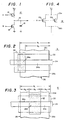
- the method for manufacturing the transistor 12 and controlling the size of its channel is illustrated in Figure 2.
- the channel of the transistor 12 is designated by the numeral 24.
- the channel is located in an active area 26 where the source is designated 26a and the drain is 26b.
- the length of the channel of an MOS transistor is typically made as small as possible.
- the width is then selected to meet the current requirement for the transistor.
- the channel is fabricated to have an initial width which is indicated as W 1 .
- the transistor 12 in a preferred embodiment receives a depletion implant 30 over an area indicated by a dashed line.
- the depletion implant 30 fully encloses the channel 24 of the transistor.
- the implant 30 is applied only to the channel region within the active area 26 due to the fabrication of oxide, not shown, above the source 26a and drain 26b.
- the depletion implant 30 is larger than the channel 24 within the transistor to ensure that the channel is fully covered.
- the depletion implant is applied to produce a pinch-off voltage (Vp) of approximately -1.0 volts. This makes transistor 12 a lightly depleted device which is utilized to drive a node, such as 14, to a full V cc .
- the scaling of the power consumption for transistor 12 is carried out as follows.
- An enhancement implant 32 shown by the area enclosed by a solid line is applied to the transistor 12.
- the enhancement implant 32 is applied by means of a mask to cover a selected portion 24a of channel 24.
- the area of the enhancement implant 32 is larger than the channel 24 to compensate for any errors of alignment in the manufacture of the integrated circuit.
- the extent of overlap of the enhancement implant over the channel determines the power scaling factor for the transistor 12. In the illustrated embodiment, approximately 20% of the channel region receives the enhancement implant. This serves to reduce the effective width of the channel 24 to that shown as W 2 .
- Approximately a 6.0 volt enhancement implant 32 is applied to the transistor 12. This results in a net implant of +5.0 volts in section 24a of the channel 24 and leaves a -1.0 volt implant in the remaining section 24b.
- the power supply V cc is typically 5.0 volts which is also the limit for the input signals A and B. Under these conditions the section 24a of channel 24 cannot be driven to a conductive state. Therefore the effective conductive width of channel 24 is that of section 24b. Since the current flow through the transistor 12 is essentially proportional to the width of the channel 24, the transistor 12 has had its current flow reduced by approximately 20%. This also corresponds to the reduction in power consumption by the transistor 12.
- the implant 32 need not fully block the source-drain current across the channel section it implants, but can be a selected level of implant to reduce the current flow across the channel section it implants.
- a polysilicon line is fabricated directly above the channel 24 to serve as a gate for the transistor.
- the implant 32 in Figure 2 is shown covering one end of the channel 24 it may also be placed in a center section of channel 24 leaving conductive portions on either side of the enhancement implant. This is shown in Figure 3.
- the implant 32 covers section 24d of the channel and does not affect sections 24c and 24e.
- the sections 24c, 24d and 24e have respective widths W 3 , W 4 and W s .
- the implant configuration shown in Figure 3 produces effectively the same result as that described in reference to Figure 2.
- FIG. 4 An equivalent circuit to the transistor 12 shown in Figure 2 is illustrated in Figure 4.
- the transistor 12 can be represented as two separate transistors having a common drain and common source.
- a transistor 12a has the source 26a and drain 26b with the channel region corresponding to section 24a.
- a transistor 12b has the source 26a and drain 26b with the channel region corresponding to section 24b.
- the transistor 12a is an enhancement device while the transistor 12b is a depletion device.
- the transistor 12a has a V T of +5.0 volts and the transistor 12b has a Vp of -1.0 volts.
- the current conductivity of transistor 12b is less than that of transistor 12 prior to the application of the enhancement implant 32. With a 5.0 volt supply the transistor 12a will not be rendered conductive. However, as noted above, the section 24a can be implanted so that transistor 12a is partially conductive.
- the size of the enhancement area 32 shown in Figure 2 can be made to cover any portion of the channel 24 desired. The greater the coverage the less will be the resulting current flow through the transistor 12 and the corresponding reduced power consumption of the transistor 12.
- the programming of the customer code is typically done by means of ion implantation in accordance with the pattern provided by the customer. At some state in the manufacturing process ion implantation is carried out to program the memory array of the circuit with the customer code.
- the method of the present invention can be easily incorporated into this programming step such that the second implantation of the channel region, enhancement implant 32, can be included in the operation of programming the customer code into the memory array of the ROM circuit.
- the method of the present invention can be easily incorporated into current ROM manufacturing techniques without the need for any additional manufacturing operations.
- the customer can further specify the speed and power consumption of his part at the same time he is specifying the bit pattern to be programmed into the memory.
- a selected embodiment of the . present invention comprises a method for scaling the speed and power consumption of an MOS transistor by controlling the effective width of the conductive channel of selected transistors by means of first and second ion implantation operations.
- the preferred application is for depletion, pull-up transistors in a read only memory circuit.
Landscapes
- Semiconductor Memories (AREA)
- Read Only Memory (AREA)
- Metal-Oxide And Bipolar Metal-Oxide Semiconductor Integrated Circuits (AREA)
- Logic Circuits (AREA)
- Power Conversion In General (AREA)
- Amplifiers (AREA)
- Insulated Gate Type Field-Effect Transistor (AREA)
Claims (6)
Priority Applications (1)
| Application Number | Priority Date | Filing Date | Title |
|---|---|---|---|
| AT82111416T ATE41077T1 (de) | 1981-12-28 | 1982-12-09 | Mos-schaltung mit bestimmtem verhaeltnis geschwindigkeit/leistung. |
Applications Claiming Priority (2)
| Application Number | Priority Date | Filing Date | Title |
|---|---|---|---|
| US33490081A | 1981-12-28 | 1981-12-28 | |
| US334900 | 1981-12-28 |
Publications (3)
| Publication Number | Publication Date |
|---|---|
| EP0082999A2 EP0082999A2 (de) | 1983-07-06 |
| EP0082999A3 EP0082999A3 (en) | 1985-04-17 |
| EP0082999B1 true EP0082999B1 (de) | 1989-03-01 |
Family
ID=23309356
Family Applications (1)
| Application Number | Title | Priority Date | Filing Date |
|---|---|---|---|
| EP82111416A Expired EP0082999B1 (de) | 1981-12-28 | 1982-12-09 | MOS-Schaltung mit bestimmtem Verhältnis Geschwindigkeit/Leistung |
Country Status (5)
| Country | Link |
|---|---|
| EP (1) | EP0082999B1 (de) |
| JP (2) | JPH0638488B2 (de) |
| AT (1) | ATE41077T1 (de) |
| CA (1) | CA1211230A (de) |
| DE (1) | DE3279496D1 (de) |
Family Cites Families (5)
| Publication number | Priority date | Publication date | Assignee | Title |
|---|---|---|---|---|
| JPS5629391B2 (de) * | 1973-05-23 | 1981-07-08 | ||
| JPS5198938A (de) * | 1975-02-26 | 1976-08-31 | ||
| US3995172A (en) * | 1975-06-05 | 1976-11-30 | International Business Machines Corporation | Enhancement-and depletion-type field effect transistors connected in parallel |
| JPS6043693B2 (ja) * | 1975-09-23 | 1985-09-30 | 株式会社東芝 | 駆動回路 |
| JPS53130987A (en) * | 1977-04-20 | 1978-11-15 | Matsushita Electric Ind Co Ltd | Semiconductor device and its manufacture |
-
1982
- 1982-12-09 AT AT82111416T patent/ATE41077T1/de active
- 1982-12-09 DE DE8282111416T patent/DE3279496D1/de not_active Expired
- 1982-12-09 EP EP82111416A patent/EP0082999B1/de not_active Expired
- 1982-12-23 CA CA000418514A patent/CA1211230A/en not_active Expired
- 1982-12-28 JP JP57227816A patent/JPH0638488B2/ja not_active Expired - Lifetime
-
1993
- 1993-01-21 JP JP5024919A patent/JPH0689987A/ja active Pending
Also Published As
| Publication number | Publication date |
|---|---|
| DE3279496D1 (en) | 1989-04-06 |
| CA1211230A (en) | 1986-09-09 |
| JPH0638488B2 (ja) | 1994-05-18 |
| EP0082999A3 (en) | 1985-04-17 |
| JPS58147073A (ja) | 1983-09-01 |
| EP0082999A2 (de) | 1983-07-06 |
| JPH0689987A (ja) | 1994-03-29 |
| ATE41077T1 (de) | 1989-03-15 |
Similar Documents
| Publication | Publication Date | Title |
|---|---|---|
| US6044018A (en) | Single-poly flash memory cell for embedded application and related methods | |
| US6239649B1 (en) | Switched body SOI (silicon on insulator) circuits and fabrication method therefor | |
| US5761121A (en) | PMOS single-poly non-volatile memory structure | |
| US5596524A (en) | CMOS memory cell with gate oxide of both NMOS and PMOS transistors as tunneling window for program and erase | |
| US5384473A (en) | Semiconductor body having element formation surfaces with different orientations | |
| US4549336A (en) | Method of making MOS read only memory by specified double implantation | |
| US6417550B1 (en) | High voltage MOS devices with high gated-diode breakdown voltage and punch-through voltage | |
| EP0776049A1 (de) | Nichtflüchtige PMOS-Speicheranordnung mit einer einzigen Polysiliziumschicht | |
| US7253047B2 (en) | Semiconductor processing methods of forming transistors, semiconductor processing methods of forming dynamic random access memory circuitry, and related integrated circuitry | |
| US6201761B1 (en) | Field effect transistor with controlled body bias | |
| US4573144A (en) | Common floating gate programmable link | |
| US5604700A (en) | Non-volatile memory cell having a single polysilicon gate | |
| US6118157A (en) | High voltage split gate CMOS transistors built in standard 2-poly core CMOS | |
| US5786618A (en) | ROM memory cell with non-uniform threshold voltage | |
| US6646919B1 (en) | Apparatus and method for margin testing single polysilicon EEPROM cells | |
| US6291862B1 (en) | Supply voltage reduction circuit for integrated circuit | |
| US5295095A (en) | Method of programming electrically erasable programmable read-only memory using particular substrate bias | |
| EP0082999B1 (de) | MOS-Schaltung mit bestimmtem Verhältnis Geschwindigkeit/Leistung | |
| US5666309A (en) | Memory cell for a programmable logic device (PLD) avoiding pumping programming voltage above an NMOS threshold | |
| US20050124119A1 (en) | Open drain input/output structure and manufacturing method thereof in semiconductor device | |
| US5319594A (en) | Semiconductor memory device including nonvolatile memory cells, enhancement type load transistors, and peripheral circuits having enhancement type transistors | |
| JPH05225778A (ja) | ワード線駆動回路 | |
| EP0472945A2 (de) | Integrierte Halbleiterschaltung | |
| JP2003007877A (ja) | Famosメモリ・セルおよび類似メモリ・セルを消去する方法 | |
| JP2005346912A (ja) | 半導体集積回路装置 |
Legal Events
| Date | Code | Title | Description |
|---|---|---|---|
| PUAI | Public reference made under article 153(3) epc to a published international application that has entered the european phase |
Free format text: ORIGINAL CODE: 0009012 |
|
| AK | Designated contracting states |
Designated state(s): AT DE FR GB NL |
|
| PUAL | Search report despatched |
Free format text: ORIGINAL CODE: 0009013 |
|
| AK | Designated contracting states |
Designated state(s): AT DE FR GB NL |
|
| 17P | Request for examination filed |
Effective date: 19851005 |
|
| 17Q | First examination report despatched |
Effective date: 19860528 |
|
| RAP1 | Party data changed (applicant data changed or rights of an application transferred) |
Owner name: THOMSON COMPONENTS-MOSTEK CORPORATION |
|
| RAP1 | Party data changed (applicant data changed or rights of an application transferred) |
Owner name: THOMSON COMPONENTS-MOSTEK CORPORATION |
|
| GRAA | (expected) grant |
Free format text: ORIGINAL CODE: 0009210 |
|
| AK | Designated contracting states |
Kind code of ref document: B1 Designated state(s): AT DE FR GB NL |
|
| REF | Corresponds to: |
Ref document number: 41077 Country of ref document: AT Date of ref document: 19890315 Kind code of ref document: T |
|
| REF | Corresponds to: |
Ref document number: 3279496 Country of ref document: DE Date of ref document: 19890406 |
|
| ET | Fr: translation filed | ||
| PG25 | Lapsed in a contracting state [announced via postgrant information from national office to epo] |
Ref country code: AT Effective date: 19891209 |
|
| PGFP | Annual fee paid to national office [announced via postgrant information from national office to epo] |
Ref country code: NL Payment date: 19891231 Year of fee payment: 8 |
|
| PLBE | No opposition filed within time limit |
Free format text: ORIGINAL CODE: 0009261 |
|
| STAA | Information on the status of an ep patent application or granted ep patent |
Free format text: STATUS: NO OPPOSITION FILED WITHIN TIME LIMIT |
|
| 26N | No opposition filed | ||
| PG25 | Lapsed in a contracting state [announced via postgrant information from national office to epo] |
Ref country code: NL Effective date: 19910701 |
|
| NLV4 | Nl: lapsed or anulled due to non-payment of the annual fee | ||
| REG | Reference to a national code |
Ref country code: GB Ref legal event code: 732E |
|
| REG | Reference to a national code |
Ref country code: FR Ref legal event code: TP |
|
| PGFP | Annual fee paid to national office [announced via postgrant information from national office to epo] |
Ref country code: GB Payment date: 19971201 Year of fee payment: 16 |
|
| PGFP | Annual fee paid to national office [announced via postgrant information from national office to epo] |
Ref country code: FR Payment date: 19971209 Year of fee payment: 16 |
|
| PGFP | Annual fee paid to national office [announced via postgrant information from national office to epo] |
Ref country code: DE Payment date: 19971212 Year of fee payment: 16 |
|
| PG25 | Lapsed in a contracting state [announced via postgrant information from national office to epo] |
Ref country code: GB Free format text: LAPSE BECAUSE OF NON-PAYMENT OF DUE FEES Effective date: 19981209 |
|
| GBPC | Gb: european patent ceased through non-payment of renewal fee |
Effective date: 19981209 |
|
| PG25 | Lapsed in a contracting state [announced via postgrant information from national office to epo] |
Ref country code: FR Free format text: LAPSE BECAUSE OF NON-PAYMENT OF DUE FEES Effective date: 19990831 |
|
| REG | Reference to a national code |
Ref country code: FR Ref legal event code: ST |
|
| PG25 | Lapsed in a contracting state [announced via postgrant information from national office to epo] |
Ref country code: DE Free format text: LAPSE BECAUSE OF NON-PAYMENT OF DUE FEES Effective date: 19991001 |