EP0081096A2 - Image rotate control circuitry - Google Patents
Image rotate control circuitry Download PDFInfo
- Publication number
- EP0081096A2 EP0081096A2 EP82110439A EP82110439A EP0081096A2 EP 0081096 A2 EP0081096 A2 EP 0081096A2 EP 82110439 A EP82110439 A EP 82110439A EP 82110439 A EP82110439 A EP 82110439A EP 0081096 A2 EP0081096 A2 EP 0081096A2
- Authority
- EP
- European Patent Office
- Prior art keywords
- display
- line
- buffer
- data
- column
- Prior art date
- Legal status (The legal status is an assumption and is not a legal conclusion. Google has not performed a legal analysis and makes no representation as to the accuracy of the status listed.)
- Ceased
Links
Images


Classifications
-
- G—PHYSICS
- G06—COMPUTING; CALCULATING OR COUNTING
- G06K—GRAPHICAL DATA READING; PRESENTATION OF DATA; RECORD CARRIERS; HANDLING RECORD CARRIERS
- G06K15/00—Arrangements for producing a permanent visual presentation of the output data, e.g. computer output printers
-
- G—PHYSICS
- G06—COMPUTING; CALCULATING OR COUNTING
- G06T—IMAGE DATA PROCESSING OR GENERATION, IN GENERAL
- G06T3/00—Geometric image transformation in the plane of the image
- G06T3/60—Rotation of a whole image or part thereof
-
- G—PHYSICS
- G06—COMPUTING; CALCULATING OR COUNTING
- G06K—GRAPHICAL DATA READING; PRESENTATION OF DATA; RECORD CARRIERS; HANDLING RECORD CARRIERS
- G06K2215/00—Arrangements for producing a permanent visual presentation of the output data
- G06K2215/0082—Architecture adapted for a particular function
- G06K2215/0091—Outputting only video data, e.g. Hard copy of CRT display
Definitions
- This invention relates to image rotate control circuitry for rotating image display data and transferring the rotated data to a printer as a horizontal print line of data.
- the present invention finds particular utility in a display copier system where displayed data is copied by a printer and particularly where the printer is operating in synchronism with the display.
- Rotation of print data is well known in the art.
- the reason for rotating the print data is generally to enable printing a longer character line than is possible if the print line is not rotated; i.e., the width of the paper in the printer is fixed whereas its length is variable, particularly when using a roll of paper or continuous forms.
- Rotation of print data is also well known in systems where the image data to be printed is serial and the printer has a plural element print head for printing data in parallel along a horizontal print line.
- Such a system is described in U. S. Patent 4,084,195. In that system; however, it is necessary to buffer the entire image and thereafter strips of the image are successively removed and stored in a horizontal strip buffer. Rotation is accomplished as alternate bytes within a given byte column are transferred from the horizontal strip buffer into one of a pair of vertical strip buffers. The alternate bytes are removed from the horizontal strip buffer in groups which are stored in registers within the rotator.
- a single random access buffer is used to store a column of image data. The column of image data, of course, does not exceed the length of the horizontal print line.
- a column of image data is stored in a buffer and then transferred serially from the buffer during vertical blanking using a divided video dot rate signal to clock the buffer to perform the transfer.
- Printing of a horizontal line takes place as the printer is strobed with a signal generated relative to the vertical sync signal.
- another column of image data is stored and transferred to the printer. The process repeats until all columns of the image have been stored and transferred to the printer.
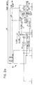
- the display copier system of Fig. 1 includes a display 100, an adapter 200 and a printer 300.
- Display 100 includes character generator 110, CRT control and timing 120, attribute control and video 140 and cathode ray tube (CRT) 150.
- the video data displayed by CRT 150 which is received from attribute control and video 140 is also applied to adapter 200 via line 145.
- CRT control and timing 120 provides timing and control signals to adapter 200 via control lines 125.
- Control lines 125 include a dot clock line 126, Fig. 2b, a vertical sync line 127 and a horizontal sync line 128.
- Adapter 200, Fig. 1 in addition to receiving inputs from display 100 also receives an input from printer 300.
- This input is in the form of a print switch signal on line 310.
- Printer 300 is substantially the same as the printer set forth in the referenced E.P.A. 12,858.
- the display 100 has more dots in a horizontal scan line than the printer 300 has print elements in the print head.
- the number of horizontal scan lines in display 100 is less than the number of print elements in the print head of printer 300.
- printer 300 as a display copier printer for display 100 by rotating the image data 90°.
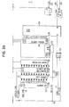
- Adapter 200 rotates the image data 90° by buffering a column of display or image data in random access storage 250, Fig. 2b.
- the video data which is displayed by CRT 150 as illustrated in Fig. 4 is in serial form on line 145 which is applied to AND circuit 201 in adapter 200, Figs. 2a and 2b.
- AND circuit 201 is conditioned by the output of compare logic 206 which compares the count value in dot counter 205 with the count value in print line or column counter 207.
- Print line counter 207 is clocked by the vertical sync signal on line 127 whereas dot counter 205 is clocked by the dot clock signal on line 126.
- the dot counter 205 is cleared by the horizontal sync signal on line 128 and the print line counter 207 is cleared by a print switch signal on line 310.
- a print switch signal is generated whenever print switch 309, Fig. 1 is activated. Basically there is a single print switch signal for a document. In this particular example there are 1320 lines per document. Thus print line counter 207 is initially cleared by the print switch signal and then counts from zero to 1319 and then is cleared again by the next print switch signal on line 310. Dot counter 205 counts from zero to 1319 for every column of image data to be printed in a horizontal print line. When the value in dot counter 205 equals the value in print line counter 207 as determined by compare logic 206, AND circuit 201 is conditioned to pass the state of the serialized video data on line 145 to the data input of trigger 203. The output of trigger 203 feeds the data input of random access storage 250.
- Random access storage 250 is addressed by the contents of address counter 240.
- address counter 240 can address 1K of storage, however, only 400 lines are displayed on CRT 150 and therefore only 400 bits of storage are required because even though there are 1320 bits in a line, only one bit from each line; i.e., a column of data is stored.
- Storages are usually commercially available in sizes other than 400 bits such as lK of storage.
- Address counter 240 is cleared by the print switch signal on line 310 or by the minus vertical sync (-V Sync) signal, these signals being applied to address counter 240 via OR circuit 239.
- the minus vertical sync signal is first applied to single shot multivibrator 235 whose output feeds OR circuit 239.
- Address counter 240 is clocked by the output of multiplexer 238 which has the vertical sync signal applied to its control input 237 which controls the passage of the plus horizontal sync signal when the control input is at a one level and the passage of the dot clock signal divided by four when the control input is at a zero level.
- Random access storage 250 is either operating in a read or a write mode.
- the read and write modes are controlled by block 230 which receives the signal from the divide by four logic block 236.
- Read/write control block 230 also receives the horizontal and vertical sync signals as well as the dot clock signal. Data is written into storage 250 at the frequency of the horizontal sync signal.
- dot counter 205 will count from zero to 1319 four hundred times; i.e., once for each horizontal scan line of the scan lines on display CRT 150.
- the value in print line counter 207 does not change until after 400 horizontal scans have been made.
- AND circuit 201 is conditioned 400 times to pass the video data on line 145 for reading into storage 250.
- Latch 225 is set and reset under control of a 10-bit binary counter 222 which is cleared by the plus vertical sync signal on line 127 and clocked by the output of divide by 128 circuit 221 which receives the dot clock signal as an input.
- Binary counter 222 is decoded by decodes 223 and 224 which feed the set and reset inputs of latch 225, respectively to generate the 5 ms strobe pulse on line 226.
- the print switch and run motor signals are shown in Fig. 3.
- Fig. 3 it is seen that there are 1320 lines of data (READ) sent to the printer 300 and each line of data contains 400 bits.
- the data line and shift register clock are each shown on two different scales. On one scale the single heavy lines represents the entire 400 bits and shift register clock. The other scale partially shows the individual bits and individual shift register clock pulses. Data is read from storage 250 much faster than when it is written therein. This is because only one video dot is written into storage for each horizontal scan during the collection of a column of video dots or data bits.
- the horizontal sync signal is also shown on a different scale.
- the video dot or data bit is written into storage 250 during the time data (write) is up; i.e., during minus horizontal sync, and the specific time depends upon which column is being collected.
- the strobe signal occurs once for each line printed and during the first part of each refresh which is controlled by the vertical sync signal.
Abstract

Description
- This invention relates to image rotate control circuitry for rotating image display data and transferring the rotated data to a printer as a horizontal print line of data.
- The present invention finds particular utility in a display copier system where displayed data is copied by a printer and particularly where the printer is operating in synchronism with the display.
- Rotation of print data is well known in the art. The reason for rotating the print data is generally to enable printing a longer character line than is possible if the print line is not rotated; i.e., the width of the paper in the printer is fixed whereas its length is variable, particularly when using a roll of paper or continuous forms.
- Rotation of print data is also well known in systems where the image data to be printed is serial and the printer has a plural element print head for printing data in parallel along a horizontal print line. Such a system is described in U. S. Patent 4,084,195. In that system; however, it is necessary to buffer the entire image and thereafter strips of the image are successively removed and stored in a horizontal strip buffer. Rotation is accomplished as alternate bytes within a given byte column are transferred from the horizontal strip buffer into one of a pair of vertical strip buffers. The alternate bytes are removed from the horizontal strip buffer in groups which are stored in registers within the rotator. In the present invention a single random access buffer is used to store a column of image data. The column of image data, of course, does not exceed the length of the horizontal print line. There is no need to buffer the entire display image and remap as in the prior art. Column one of the display is printed as horizontal line one and this process repeats until all columns of the display are printed as horizontal lines. For further simplicity the printer is strobed by and receives clocks from the display whereby it operates in synchronism with the display but at its refresh rate. That is for each full image display, one horizontal line of printing is developed and transferred to the printer during vertical blanking and then a new horizontal line of printing is developed during refresh. The image is successively refreshed until all columns of image data have been printed as horizontal rows. Other prior art for manipulating image data by 90° rotation but having the need to buffer the entire image includes U. S. Patents 3,924,225 and 3,976,982.
- A column of image data is stored in a buffer and then transferred serially from the buffer during vertical blanking using a divided video dot rate signal to clock the buffer to perform the transfer. Printing of a horizontal line takes place as the printer is strobed with a signal generated relative to the vertical sync signal. During the next refresh of the image another column of image data is stored and transferred to the printer. The process repeats until all columns of the image have been stored and transferred to the printer.
-
- Fig. 1 is a schematic diagram illustrating an image display copier system incorporating the present invention;
- Figs. 2a and 2 b with Fig. 2a disposed above Fig. 2b taken together are a schematic diagram illustrating the adapter shown in block form in Fig. 1;
- Fig. 3 is a timing diagram; and
- Fig. 4 is a diagram illustrating the display image and the printed output.
- With reference to the drawings and particularly to Fig. 1 the invention is illustrated by way of example as being incorporated in a display copier system shown and described in E.P.A. No. 12,858. The display copier system of Fig. 1 includes a
display 100, anadapter 200 and aprinter 300.Display 100 includes character generator 110, CRT control andtiming 120, attribute control andvideo 140 and cathode ray tube (CRT) 150. The video data displayed by CRT 150 which is received from attribute control andvideo 140 is also applied to adapter 200 vialine 145. CRT control andtiming 120 provides timing and control signals to adapter 200 viacontrol lines 125.Control lines 125 include adot clock line 126, Fig. 2b, avertical sync line 127 and ahorizontal sync line 128. -
Adapter 200, Fig. 1, in addition to receiving inputs fromdisplay 100 also receives an input fromprinter 300. This input is in the form of a print switch signal online 310.Printer 300 is substantially the same as the printer set forth in the referenced E.P.A. 12,858. Thedisplay 100, however, has more dots in a horizontal scan line than theprinter 300 has print elements in the print head. The number of horizontal scan lines indisplay 100; however, is less than the number of print elements in the print head ofprinter 300. Thus it is possible to useprinter 300 as a display copier printer fordisplay 100 by rotating the image data 90°. -
Adapter 200 rotates the image data 90° by buffering a column of display or image data inrandom access storage 250, Fig. 2b. The video data which is displayed by CRT 150 as illustrated in Fig. 4 is in serial form online 145 which is applied to ANDcircuit 201 inadapter 200, Figs. 2a and 2b. ANDcircuit 201 is conditioned by the output of comparelogic 206 which compares the count value in dot counter 205 with the count value in print line orcolumn counter 207.Print line counter 207 is clocked by the vertical sync signal online 127 whereas dot counter 205 is clocked by the dot clock signal online 126. The dot counter 205 is cleared by the horizontal sync signal online 128 and theprint line counter 207 is cleared by a print switch signal online 310. - A print switch signal is generated whenever print switch 309, Fig. 1 is activated. Basically there is a single print switch signal for a document. In this particular example there are 1320 lines per document. Thus
print line counter 207 is initially cleared by the print switch signal and then counts from zero to 1319 and then is cleared again by the next print switch signal online 310. Dot counter 205 counts from zero to 1319 for every column of image data to be printed in a horizontal print line. When the value in dot counter 205 equals the value inprint line counter 207 as determined by comparelogic 206, ANDcircuit 201 is conditioned to pass the state of the serialized video data online 145 to the data input oftrigger 203. The output oftrigger 203 feeds the data input ofrandom access storage 250.Random access storage 250 is addressed by the contents ofaddress counter 240. In this particular example,address counter 240 can address 1K of storage, however, only 400 lines are displayed onCRT 150 and therefore only 400 bits of storage are required because even though there are 1320 bits in a line, only one bit from each line; i.e., a column of data is stored. Storages, however, are usually commercially available in sizes other than 400 bits such as lK of storage. -
Address counter 240 is cleared by the print switch signal online 310 or by the minus vertical sync (-V Sync) signal, these signals being applied to address counter 240 via ORcircuit 239. The minus vertical sync signal is first applied tosingle shot multivibrator 235 whose output feeds ORcircuit 239.Address counter 240 is clocked by the output ofmultiplexer 238 which has the vertical sync signal applied to itscontrol input 237 which controls the passage of the plus horizontal sync signal when the control input is at a one level and the passage of the dot clock signal divided by four when the control input is at a zero level. -
Random access storage 250 is either operating in a read or a write mode. The read and write modes are controlled byblock 230 which receives the signal from the divide by fourlogic block 236. Read/write control block 230 also receives the horizontal and vertical sync signals as well as the dot clock signal. Data is written intostorage 250 at the frequency of the horizontal sync signal. For example, dot counter 205 will count from zero to 1319 four hundred times; i.e., once for each horizontal scan line of the scan lines ondisplay CRT 150. The value inprint line counter 207 does not change until after 400 horizontal scans have been made. Thus there are 400 comparisons and ANDcircuit 201 is conditioned 400 times to pass the video data online 145 for reading intostorage 250. - After one vertical column of video data has been stored in
storage 250 there is a vertical retrace or blanking ofdisplay 100 and then the display is refreshed. During the vertical retrace or blanking data is read fromstorage 250 and transferred to shiftregisters printer 300, Fig. 1. The output ofstorage 250 is applied to a twobit shift register 251 which is clocked by the output ofmultiplexer 238. The output ofmultiplexer 238 is divided by two bylogic block 252 to provide a shift register clock signal online 253. Both the odd and even outputs fromshift register 251 are sent tobuffers printer 300 onlines adapter 200 online 226 fromlatch 225. -
Latch 225 is set and reset under control of a 10-bitbinary counter 222 which is cleared by the plus vertical sync signal online 127 and clocked by the output of divide by 128circuit 221 which receives the dot clock signal as an input.Binary counter 222 is decoded bydecodes latch 225, respectively to generate the 5 ms strobe pulse online 226. - As a horizontal line is being printed by
printer 300 the next line to be printed is being collected and stored instorage 250 in the manner previously described but with print line counter having been advanced by the vertical sync signal. Thus the next column of image data is stored bystorage 250. In this particular example there are 1320 columns to be printed as horizontal lines. Thus whenprint line counter 207 reaches 1319 as determined bybinary decode line 310 will be reset to causemotor 351 inprinter 300 to stop.Latch 209 provides a minus run motor signal online 210 tomotor 351, Fig. 1. - The print switch and run motor signals are shown in Fig. 3. In Fig. 3 it is seen that there are 1320 lines of data (READ) sent to the
printer 300 and each line of data contains 400 bits. The data line and shift register clock are each shown on two different scales. On one scale the single heavy lines represents the entire 400 bits and shift register clock. The other scale partially shows the individual bits and individual shift register clock pulses. Data is read fromstorage 250 much faster than when it is written therein. This is because only one video dot is written into storage for each horizontal scan during the collection of a column of video dots or data bits. The horizontal sync signal is also shown on a different scale. The video dot or data bit is written intostorage 250 during the time data (write) is up; i.e., during minus horizontal sync, and the specific time depends upon which column is being collected. The strobe signal occurs once for each line printed and during the first part of each refresh which is controlled by the vertical sync signal.
Claims (8)
Applications Claiming Priority (2)
| Application Number | Priority Date | Filing Date | Title |
|---|---|---|---|
| US06/327,307 US4467448A (en) | 1981-12-04 | 1981-12-04 | Image rotate control circuitry |
| US327307 | 1981-12-04 |
Publications (2)
| Publication Number | Publication Date |
|---|---|
| EP0081096A2 true EP0081096A2 (en) | 1983-06-15 |
| EP0081096A3 EP0081096A3 (en) | 1984-04-25 |
Family
ID=23276023
Family Applications (1)
| Application Number | Title | Priority Date | Filing Date |
|---|---|---|---|
| EP82110439A Ceased EP0081096A3 (en) | 1981-12-04 | 1982-11-12 | Image rotate control circuitry |
Country Status (3)
| Country | Link |
|---|---|
| US (1) | US4467448A (en) |
| EP (1) | EP0081096A3 (en) |
| JP (1) | JPS5898263A (en) |
Cited By (3)
| Publication number | Priority date | Publication date | Assignee | Title |
|---|---|---|---|---|
| EP0137147A2 (en) * | 1983-09-30 | 1985-04-17 | International Business Machines Corporation | Pattern processing system |
| GB2154348A (en) * | 1984-02-15 | 1985-09-04 | Citizen Watch Co Ltd | Bit pattern conversion apparatus |
| US5733051A (en) * | 1992-06-11 | 1998-03-31 | Esselte N.V. | Label printing apparatus |
Families Citing this family (16)
| Publication number | Priority date | Publication date | Assignee | Title |
|---|---|---|---|---|
| CA1252902A (en) * | 1985-10-31 | 1989-04-18 | David R. Pruett | Method for rotating a binary image |
| US5093906A (en) * | 1986-03-05 | 1992-03-03 | Unisys Corporation | Text orientation system for dot matrix printers |
| GB2229835B (en) * | 1989-03-07 | 1993-03-24 | Brother Ind Ltd | Text processing device |
| US4977519A (en) * | 1989-07-12 | 1990-12-11 | Ricoh Company, Ltd. | Laser printer controller flexible frame buffer architecture which allows software to change X and Y dimensions of the buffer |
| US4984182A (en) * | 1989-07-12 | 1991-01-08 | Ricoh Company, Ltd. | Laser printer controller flexible frame buffer achitecture which allows software to initiate the loading of a frame buffer start address |
| US6115543A (en) * | 1989-11-01 | 2000-09-05 | Canon Kabushiki Kaisha | Data communication apparatus having a handy scanner |
| US5199101A (en) * | 1990-10-03 | 1993-03-30 | Bell & Howell Publication Systems Company | On the fly image rotation system for high-speed printers |
| US5299310A (en) * | 1992-01-15 | 1994-03-29 | Ricoh Company, Ltd. | Flexible frame buffer for raster output devices |
| JPH06290016A (en) * | 1993-03-31 | 1994-10-18 | Fujitsu Ltd | Display device for face-to-face dealing and its control method |
| US5870536A (en) * | 1995-07-11 | 1999-02-09 | Canon Kabushiki Kaisha | Data conversion apparatus and image recording apparatus |
| US5634088A (en) * | 1995-11-01 | 1997-05-27 | Xerox Corporation | Method and apparatus for rotation of high addressability bitmap images |
| US6226016B1 (en) * | 1996-02-05 | 2001-05-01 | Seiko Epson Corporation | Display apparatus and method capable of rotating an image by 180 degrees |
| US5870581A (en) * | 1996-12-20 | 1999-02-09 | Oak Technology, Inc. | Method and apparatus for performing concurrent write operations to a single-write-input register file and an accumulator register |
| US5946222A (en) * | 1996-12-20 | 1999-08-31 | Oak Technology, Inc. | Method and apparatus for performing a masked byte addition operation |
| US6223181B1 (en) | 1997-07-31 | 2001-04-24 | Oak Technology, Inc. | Memory conserving and compression technique-compatible image rotation system |
| US9087337B2 (en) * | 2008-10-03 | 2015-07-21 | Google Inc. | Displaying vertical content on small display devices |
Citations (6)
| Publication number | Priority date | Publication date | Assignee | Title |
|---|---|---|---|---|
| DE2153884A1 (en) * | 1970-10-30 | 1972-05-04 | Agfa Gevaert Ag | Method and apparatus for registering two-dimensional patterns |
| US3924225A (en) * | 1973-05-30 | 1975-12-02 | Olympia Werke Ag | Character display dot raster signal generator provided with character memory |
| US4084195A (en) * | 1976-12-30 | 1978-04-11 | International Business Machines Corporation | Image data remapping system |
| FR2443335A1 (en) * | 1978-12-06 | 1980-07-04 | Cii Honeywell Bull | RECORDING CONTROL DEVICE FOR POINT RECORDING MACHINE |
| EP0012858A1 (en) * | 1978-12-26 | 1980-07-09 | International Business Machines Corporation | Display and recording apparatus |
| EP0013709A1 (en) * | 1979-01-18 | 1980-08-06 | Robert Bosch Gmbh | Method for recording an information consisting of a plurality of alphanumeric characters |
Family Cites Families (4)
| Publication number | Priority date | Publication date | Assignee | Title |
|---|---|---|---|---|
| US3918041A (en) * | 1974-08-05 | 1975-11-04 | Roger A Mao | Multiplex display system |
| US3976982A (en) * | 1975-05-12 | 1976-08-24 | International Business Machines Corporation | Apparatus for image manipulation |
| US4158203A (en) * | 1977-09-30 | 1979-06-12 | Buckeye International, Inc. | Arrangement for recording images appearing on a cathode ray tube |
| JPS55127682A (en) * | 1979-03-24 | 1980-10-02 | Hitachi Ltd | Crt hard copy unit |
-
1981
- 1981-12-04 US US06/327,307 patent/US4467448A/en not_active Expired - Fee Related
-
1982
- 1982-10-13 JP JP57178615A patent/JPS5898263A/en active Granted
- 1982-11-12 EP EP82110439A patent/EP0081096A3/en not_active Ceased
Patent Citations (6)
| Publication number | Priority date | Publication date | Assignee | Title |
|---|---|---|---|---|
| DE2153884A1 (en) * | 1970-10-30 | 1972-05-04 | Agfa Gevaert Ag | Method and apparatus for registering two-dimensional patterns |
| US3924225A (en) * | 1973-05-30 | 1975-12-02 | Olympia Werke Ag | Character display dot raster signal generator provided with character memory |
| US4084195A (en) * | 1976-12-30 | 1978-04-11 | International Business Machines Corporation | Image data remapping system |
| FR2443335A1 (en) * | 1978-12-06 | 1980-07-04 | Cii Honeywell Bull | RECORDING CONTROL DEVICE FOR POINT RECORDING MACHINE |
| EP0012858A1 (en) * | 1978-12-26 | 1980-07-09 | International Business Machines Corporation | Display and recording apparatus |
| EP0013709A1 (en) * | 1979-01-18 | 1980-08-06 | Robert Bosch Gmbh | Method for recording an information consisting of a plurality of alphanumeric characters |
Cited By (7)
| Publication number | Priority date | Publication date | Assignee | Title |
|---|---|---|---|---|
| EP0137147A2 (en) * | 1983-09-30 | 1985-04-17 | International Business Machines Corporation | Pattern processing system |
| EP0137147A3 (en) * | 1983-09-30 | 1985-05-22 | International Business Machines Corporation | Pattern processing system |
| GB2154348A (en) * | 1984-02-15 | 1985-09-04 | Citizen Watch Co Ltd | Bit pattern conversion apparatus |
| US4691364A (en) * | 1984-02-15 | 1987-09-01 | Citizen Watch Co., Ltd. | Bit pattern conversion apparatus |
| US5733051A (en) * | 1992-06-11 | 1998-03-31 | Esselte N.V. | Label printing apparatus |
| US5967679A (en) * | 1992-06-11 | 1999-10-19 | Esselte N.V. | Label printing apparatus |
| US6079889A (en) * | 1992-06-11 | 2000-06-27 | Esselte N.V. | Label printing apparatus |
Also Published As
| Publication number | Publication date |
|---|---|
| JPS5898263A (en) | 1983-06-11 |
| US4467448A (en) | 1984-08-21 |
| JPS6367190B2 (en) | 1988-12-23 |
| EP0081096A3 (en) | 1984-04-25 |
Similar Documents
| Publication | Publication Date | Title |
|---|---|---|
| US4467448A (en) | Image rotate control circuitry | |
| EP0153197B1 (en) | A method of operating a display system | |
| US4417239A (en) | Interactive combination display | |
| US3634828A (en) | Graphical data processing apparatus | |
| EP0321491B1 (en) | Print engine drive interface | |
| US4075620A (en) | Video display system | |
| US4486856A (en) | Cache memory and control circuit | |
| US4399435A (en) | Memory control unit in a display apparatus having a buffer memory | |
| US3685038A (en) | Video data color display system | |
| US4455554A (en) | Proportionality in minature displays | |
| EP0215984B1 (en) | Graphic display apparatus with combined bit buffer and character graphics store | |
| US4378594A (en) | High speed to low speed data buffering means | |
| EP0140555B1 (en) | Apparatus for displaying images defined by a plurality of lines of data | |
| EP0120142B1 (en) | Graphic display system | |
| US4937565A (en) | Character generator-based graphics apparatus | |
| US4418345A (en) | Displaying a full page representation | |
| EP0186070A2 (en) | Apparatus for distortion free clearing of a display during a single frame time | |
| US4500928A (en) | Storage apparatus for video data | |
| GB2185608A (en) | Laser printer control system | |
| US5012232A (en) | Bit mapped memory plane with character attributes for video display | |
| EP0092995B1 (en) | Method and apparatus for reading and writing display data | |
| EP0283579A2 (en) | Raster scan display system with random access memory character generator | |
| JP2564513B2 (en) | Printer control device | |
| SU1741123A1 (en) | Apparatus for representing information | |
| JPS60159789A (en) | Display memory control system |
Legal Events
| Date | Code | Title | Description |
|---|---|---|---|
| PUAI | Public reference made under article 153(3) epc to a published international application that has entered the european phase |
Free format text: ORIGINAL CODE: 0009012 |
|
| AK | Designated contracting states |
Designated state(s): DE FR GB |
|
| 17P | Request for examination filed |
Effective date: 19831021 |
|
| PUAL | Search report despatched |
Free format text: ORIGINAL CODE: 0009013 |
|
| AK | Designated contracting states |
Designated state(s): DE FR GB |
|
| STAA | Information on the status of an ep patent application or granted ep patent |
Free format text: STATUS: THE APPLICATION HAS BEEN REFUSED |
|
| 18R | Application refused |
Effective date: 19890203 |
|
| REG | Reference to a national code |
Ref country code: GB Ref legal event code: 732 |
|
| APAF | Appeal reference modified |
Free format text: ORIGINAL CODE: EPIDOSCREFNE |
|
| RIN1 | Information on inventor provided before grant (corrected) |
Inventor name: SENDELBACH, LEE ANTON Inventor name: REGEHR, JOHN LEON |