EP0079805A2 - Gehäuse für Fernmeldeeinrichtung - Google Patents
Gehäuse für Fernmeldeeinrichtung Download PDFInfo
- Publication number
- EP0079805A2 EP0079805A2 EP82306120A EP82306120A EP0079805A2 EP 0079805 A2 EP0079805 A2 EP 0079805A2 EP 82306120 A EP82306120 A EP 82306120A EP 82306120 A EP82306120 A EP 82306120A EP 0079805 A2 EP0079805 A2 EP 0079805A2
- Authority
- EP
- European Patent Office
- Prior art keywords
- printed
- jack
- printed circuit
- circuit board
- board
- Prior art date
- Legal status (The legal status is an assumption and is not a legal conclusion. Google has not performed a legal analysis and makes no representation as to the accuracy of the status listed.)
- Granted
Links
Images


Classifications
-
- H—ELECTRICITY
- H01—ELECTRIC ELEMENTS
- H01R—ELECTRICALLY-CONDUCTIVE CONNECTIONS; STRUCTURAL ASSOCIATIONS OF A PLURALITY OF MUTUALLY-INSULATED ELECTRICAL CONNECTING ELEMENTS; COUPLING DEVICES; CURRENT COLLECTORS
- H01R12/00—Structural associations of a plurality of mutually-insulated electrical connecting elements, specially adapted for printed circuits, e.g. printed circuit boards [PCB], flat or ribbon cables, or like generally planar structures, e.g. terminal strips, terminal blocks; Coupling devices specially adapted for printed circuits, flat or ribbon cables, or like generally planar structures; Terminals specially adapted for contact with, or insertion into, printed circuits, flat or ribbon cables, or like generally planar structures
- H01R12/70—Coupling devices
- H01R12/71—Coupling devices for rigid printing circuits or like structures
- H01R12/75—Coupling devices for rigid printing circuits or like structures connecting to cables except for flat or ribbon cables
-
- H—ELECTRICITY
- H01—ELECTRIC ELEMENTS
- H01R—ELECTRICALLY-CONDUCTIVE CONNECTIONS; STRUCTURAL ASSOCIATIONS OF A PLURALITY OF MUTUALLY-INSULATED ELECTRICAL CONNECTING ELEMENTS; COUPLING DEVICES; CURRENT COLLECTORS
- H01R12/00—Structural associations of a plurality of mutually-insulated electrical connecting elements, specially adapted for printed circuits, e.g. printed circuit boards [PCB], flat or ribbon cables, or like generally planar structures, e.g. terminal strips, terminal blocks; Coupling devices specially adapted for printed circuits, flat or ribbon cables, or like generally planar structures; Terminals specially adapted for contact with, or insertion into, printed circuits, flat or ribbon cables, or like generally planar structures
-
- H—ELECTRICITY
- H05—ELECTRIC TECHNIQUES NOT OTHERWISE PROVIDED FOR
- H05K—PRINTED CIRCUITS; CASINGS OR CONSTRUCTIONAL DETAILS OF ELECTRIC APPARATUS; MANUFACTURE OF ASSEMBLAGES OF ELECTRICAL COMPONENTS
- H05K7/00—Constructional details common to different types of electric apparatus
- H05K7/14—Mounting supporting structure in casing or on frame or rack
- H05K7/1438—Back panels or connecting means therefor; Terminals; Coding means to avoid wrong insertion
- H05K7/1447—External wirings; Wiring ducts; Laying cables
Definitions
- the present invention relates to a housing device for housing communication circuits and equipment such as data circuits for transmitting various data, telephone circuits, and facsimile circuits.
- a plurality of printed circuit board units which convert data or sounds to transmission signals are housed within a rack of a communication apparatus.
- Outer main circuit cables which connect. the printed circuit board units with units of another communication apparatus and inner distribution cables for supplying power and connecting the printed circuit board to the ground or to an alarm line are arranged within the rack.
- a test jack socket is mounted on the front end of the printed circuit board to enable the function of the printed circuit board to be tested and to check the connection between the printed circuit board and the circuit cables. It is desirable that the housing or rack of such a communication apparatus is simple in construction so that it can be easily assembled and desirable that it occupies a small area.
- Wiring patterns which connect the test jack socket on the front end of the printed circuit board and the connectors on the rear end of the printed board are formed on the printed circuit board. These wiring patterns occupy a space on the printed circuit board, and therefore, the space for mounting electronic parts or wiring patterns for communication circuits on the printed board is decreased.
- a housing device housing communication circuits and equipment comprising a frame which receives a plurality of printed circuit boards circuit cables arranged along it and connectors mounted on it, each of the printed circuit boards including a communication circuit, a test jack socket for testing arranged at its front end and a connector arranged at its rear end and connected to the connectors mounted on the frame, the jack sockets including first and second connection leads mounted in a moulded body having an opening at the front of the printed circuit board so that a co-operating jack plug can be inserted in a direction parallel with the printed circuit board, the first and second connecting leads being formed so that they contact one another adjacent the opening in the absence of the jack plug and so that they are separate from each other at the rear of the jack socket and project out of the moulded body, is characterised in that the first connecting lead of each jack socket is connected to the communication circuit formed on its printed circuit board and in that the second conn- ! ecting lead of each jack socket is directly connected to one of the circuit cables.
- a test jack device 102 is mounted on the front end of a printed board 101.
- a connector 104 is mounted on the rear end of the printed board 10.
- the connector 104 is coupled with a connector 105 which is mounted on the rack frame (not shown).
- the connector 105 is connected to an inner wiring cable 106 which is disposed along the frame.
- the inner wiring cable 106 comprises electric lines which are common to the printed boards within the rack, such as a power line, a ground line, and an alarm line.
- the test jack device 102 comprises two leads 107 and 108.
- the first lead 107 is connected to a communication circuit 103, which comprises electronic parts (not shown), by a wiring pattern 109 printed on the printed board 101.
- the circuit 103 is connected to the connector 104 by a wiring pattern 109' printed on the printed board 101.
- the second lead 108 is connected to a connector 110, which is attached to an end of an outer cable 111, which deviates from a main cable 112 comprising signal lines connected to a centre office or another communication apparatus.
- a horizontal section of a housing device according to the present invention is illustrated in Fig. 2.
- a rack frame 211 extends longitudinally in a direction perpendicular to the drawing.
- Main cables 212 are disposed along the frame 211.
- a frame connector 213 is mounted on the frame 211.
- a unit connector 213' which is coupled with the frame connector 213, is mounted on the rear end of a printed board 214, which constitutes a printed board unit.
- a test jack device 216 for testing the function of the circuit of the printed board 214 and for checking the connection between the circuit and the outer cables is mounted on the front end of the printed board 214.
- the test jack device 216 is connected to electronic parts (not shown) on the printed board 214 by the printed pattern (not shown) formed thereon.
- the test jack device 216 is connected to an outer cable 217, which is separated from one of the main cables 212 by a cable connector 215 attached to the end of the outer cable 217.
- a plurality of printed boards 214 are
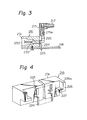
- the test jack device 216 is illustrated in detail in Figs. 3 and 4.
- the test jack device 216 comprises a plurality of jacks 230, each of which comprises a first lead 224 and a second lead 225 within a molded body 231.
- the opening of the jack 230 is disposed at the front side of the molded body 231.
- the insertion direction of the jack 230 is parallel to the printed board 214.
- the first and second leads 224 and 225 contact each other at the neck 232 of the jack 230 and seaprate from each other at the rear of the jack 230. Both leads 224 and 225 project out of the molded body 231 from the rear side thereof.
- the first lead 224 is folded toward the printed board 214 so as to be connected to the printed pattern formed thereon.
- the first lead 224 is easily secured to the printed board by the solder dip method, in which the lower side of the printed board 214 is dipped in molten solder.
- Reference numeral 233 designates the solder.
- the second lead 225 is foled upward.
- a jack 215a of the cable connector 215 is connected to the end of the second lead 225.
- a guide wall 226 is formed on each side of the rear face of thw molded body 231 so as to guide the cable connector 215.
- the guide wall 226 comrises a guide face 226a and a stop surface 227.
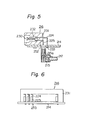
- test jack device Another example of the test jack device according to the present invention is illustrated in Figs. 5, 6, and 7.
- the first and second leads 224 and 225 are folded in the same direction, that is, toward the printed board"214.
- An opening 252 is formed in the printed board 214 for insertion of the cable connector 215 attached to the end of the outer circuit cable 217.
- the tip of the second lead 225 is positioned above the printed board surface so as to avoid wetting of the second lead 225 with solder at the time of soldering by means of the solder dip method.
- Each of the first and second leads 224 and 225 is punched from a plate, assembled on the molded body 231, and is then folded in the direction of the arrow A in Fig. 8, in which'only the second lead 225 is illustrated.
- the outer view and the inner view of the housing device according to the present invention are illustrated in Figs. 9 and 10, respectively.
- a plurality of printed board units 3 are disposed along a frame 1.
- the test jack of Fig. 5 is installed in each of the printed board unit 3.
- the printed board units 3 are covered by a cover 2.
- Each printed board unit 3 comprises a front cover 4, a printed board assembly 5, and a shelf 6, as illustrated in Fig. 10.
- the front cover 4 has an opening 7 for the insertion of a plug so that a test plug (not-shown) can be connected with a test jack device 10.
- the printed board assembly 5 comprises a printed board 8 held by upper and lower support members 9.
- the test jack device 10 is mounted on the front end of the printed board 8.
- a unit connector 11 for connecting the printed board with an inner wiring cable, which comprises a flat flexible cable 14, is mounted on the rear end of the printed board 8.
- the shelf 6 comprises an outer case 19, which has a cable support 12 and an opening 13 on the side surface thereof for the insertion of a cable connector 20 and a draught hole 31 on the upper surface thereof.
- Main circuit cables 18 are disposed along the frame 1. Each main circuit cable 18 is connected to the test jack device 10 by the cable connector 20 through the opening 13.
- the flat cable 14, which is used as an inner cable, comprises electrical lines common to the printed boards within the rack (housing device), such as a power line, a ground line, and an alarm line.
- the flat cable 14 is made of a flexible printed board and is disposed along the inside of the frame 1.
- Frame connectrors 15 are attached to the flat cable 14 at predetermined positions corresponding to the positions of the printed board unit 3.
- a projection 17 of the cover 2 is inserted into a hole 16 of the frame 1 and then the cover is secured to the frame 1 by means of a screw 32.
- the printed board unit 3 and the frame 1 of Fig. 10 are illustrated in detail in Fig. 11.
- the printed board 8 is held in a groove 9a of each support member 9 so as to form a printed board assembly 5.
- the test jack device 10 has a opening 10a at the front end thereof so as to receive a test plug (not shown).
- the test jack device 10 has leads 22 to which the cable connector 20 of the outer main cable 18 (Fig. 10) is connected.
- the printed board assembly 5 is housed in the shelf 6.
- the shelf 6 is secured to the frame 1 by screwing screw bars 26 into holes 27 of the frame 1.
- the front cover 4 is secured to the shelf 6 by screwing a screw 24 into a tongue 25 of the shelf 6 at the upper and lower portions thereof.
- Projections 29 are formed in the rear portion of the shelf 6. Each projection 29 fits into a hole 28 of the frame 1 so as to hold the shelf 6 on the frame 1. Draught opening 30 are provided in the frame 1.
- the support member 9 is illustrated in detail in Fig. 12.
- the support member 9 is a mold of plastic material.
- the upper and the lower support members are identical.
- the support member 9 comprises frames 9d, each of which has a groove 9a for holding the printed board, and frames 9c which are connected to the frames 9d.
- a space 40 between the frames 9d serves as a draught hole.
- Notches 9b are provided on the frame 9c for easy cutting of the frame 9c and correspond to the number of printed boards to be housed,
- a projection 9e is provided on each inside surface of the groove 9a, as illustrated in Fig. 13.
- the printed board 8 is pushed into the groove 9a, which is elastically widened, and then the projections are fetted into an opening 8a of the printed board 8 so that the printed board 8 is securely held by the support member 9.
- the length of the support member 9 in the direction perpendicular to the printed board 8 above its surface is larger than the height of the electronic parts 42 mounted on the surface, as illustrated in Fig. 15. Also, the length of the support member 9 above the surface opposite to the surface on which parts are mounted is larger than the height of the solder 41 of the lead of each electronic part.
- the printed board 8 is stored in the form of a printed board assembly assembled with the support member 9. Therefore, the electronic parts 42 and the lead tip are protected by the support member 9 in any storage position of the assembly, as illustrated in Fig. 15(a), (b), and (c).
- Figure 16 is a horizontal sectional view of the housing device of Fig. 9.
- the test jack device 10 has a first lead 33 which is connected to a printed pattern (not shown) formed on the printed board 8 and a second lead 22 which is connected to the cable connector 20 at the end of the outer main circuit cable 18.
- the unit connector 11 at the rear end of the printed board 8 is coupled with the frame connector 15, which is connected to the flat cable 14 for wiring a power supply line, a ground line, and an alarm line.
- a plurality of frame connectors 15 can be attached to the flat cable 14 by appropriately folding the flat cable 14, as illustrated in Fig. 17.
- the printed board unit of Fig. 19 comprises two printed boards 8 and 8 1 .
- Two frame connectors 15 and 15' are disposed side by side on the flat cable 14.
- the main cable (not shown) is connected to the test jack device (not shown) of the printed board 8 on the right side thereof.
- the printed board unit of Fig. 18 comprises one printed board 8.
- the test jack device includes first and second leads, the first lead being connected to the circuit formed on the printed board and the second lead being directly connected to the main circuit cable so that the circuit on the printed board is connected to the outer main circuit cable by the test jack device. Therefore, patterns for connecting the test jack device and the main cable are not printed on the printed board, with the result that the space for the communication circuit on the printed board is increased and the entire area of the printed board can be effectively used for the communication circuit.
- the number of connectors between the outer main cable and the printed board is decreased, and the number of connection pins of the unit connector at the rear end of the printed board is also decreased since the unit connector is used to connect the printed board and the inner wiring cable, which does not include outer signal lines.
- the cost of connectors is lowered, the backboard can be omitted, and the construction can be simplified.
- the reliability of the connection is increased since the number of connectors is decreased.
- compling of the cable connector and the test jack device is easily and securely achieved because of the guide wall of the molded body.
- the opening 252 of the printed board 214 serves as a guide for the second lead 225.
- the printed board is assembled with the molded support member of plastic material before it is housed in the shelf, thereby making it possible to simplify the shelf structure and to easily attach the shelf to the frame.
- the printed board is easily and securely held by the support member due to the elasticity thereof and does not necessitate the use of bolts or screws.
- Guide grooves for the printed board are unnecessary in the shelf, thereby making it possible tc further simplify the shelf structure.
- the shelf can be made less stiff since the shelf does not directly hold the printed board. Therefore, a large opening for draught can be formed in the shelf, thereby upgrading the efficiency of heat radiation.
- the printed board is protected by the support member if it is stored without a special protection case.
- the use of a flexible flat cable as a distribution cable within the rack makes it possible to omit the backboard and simplify the rack structure.
- the rack can be easily assembled and be made small. Omission of the backboard makes it possible to form draught openings on the frame. Therefore, the frame can be used as a convection passage so as to upgrade the efficiency of heat dissipation.
Applications Claiming Priority (6)
| Application Number | Priority Date | Filing Date | Title |
|---|---|---|---|
| JP18364681A JPS5885598A (ja) | 1981-11-18 | 1981-11-18 | 通信回線機器収容装置 |
| JP183646/81 | 1981-11-18 | ||
| JP184361/81 | 1981-11-19 | ||
| JP18436181A JPS58108796A (ja) | 1981-11-19 | 1981-11-19 | 通信回線機器収容装置 |
| JP18611681A JPS58108798A (ja) | 1981-11-21 | 1981-11-21 | 通信回線機器収容装置の測定ジヤツク構造 |
| JP186116/81 | 1981-11-21 |
Publications (3)
| Publication Number | Publication Date |
|---|---|
| EP0079805A2 true EP0079805A2 (de) | 1983-05-25 |
| EP0079805A3 EP0079805A3 (en) | 1983-06-22 |
| EP0079805B1 EP0079805B1 (de) | 1986-03-19 |
Family
ID=27325315
Family Applications (1)
| Application Number | Title | Priority Date | Filing Date |
|---|---|---|---|
| EP82306120A Expired EP0079805B1 (de) | 1981-11-18 | 1982-11-17 | Gehäuse für Fernmeldeeinrichtung |
Country Status (3)
| Country | Link |
|---|---|
| US (1) | US4510552A (de) |
| EP (1) | EP0079805B1 (de) |
| DE (1) | DE3270022D1 (de) |
Cited By (1)
| Publication number | Priority date | Publication date | Assignee | Title |
|---|---|---|---|---|
| CN105706440A (zh) * | 2013-11-12 | 2016-06-22 | 汤姆逊许可公司 | 通过pcb孔的电缆引线穿管 |
Families Citing this family (12)
| Publication number | Priority date | Publication date | Assignee | Title |
|---|---|---|---|---|
| FR2544556B1 (fr) * | 1983-04-15 | 1985-07-05 | Telemecanique Electrique | Dispositif entree/sortie pour automate programmable, gamme de tels dispositifs et procede pour realiser leur bornier |
| FR2550042B1 (fr) * | 1983-07-29 | 1985-11-22 | Ctm | Dispositif de raccordement modulaire pour repartiteur telephonique |
| IN164043B (de) * | 1984-05-21 | 1988-12-31 | Siemens Ag | |
| US4840568A (en) * | 1987-03-31 | 1989-06-20 | Adc Telecommunications, Inc. | Jack assembly |
| FR2649550B1 (de) * | 1989-07-06 | 1991-10-11 | Telemecanique | |
| US5014164A (en) * | 1989-09-08 | 1991-05-07 | International Business Machines Corporation | Cable organizer |
| FR2683970B1 (fr) * | 1991-11-14 | 1996-03-01 | Telemecanique | Ensemble electronique modulaire. |
| US6632106B2 (en) | 2001-07-24 | 2003-10-14 | Adc Telecommunications, Inc. | Jack; jack assembly; and methods |
| US6554652B1 (en) | 2002-02-15 | 2003-04-29 | Adc Telecommunications, Inc. | Jack assembly including baluns interface; and methods |
| US20060030210A1 (en) * | 2004-02-09 | 2006-02-09 | Willing Steven L | Sealed cartridge electrical interconnect |
| US20090181571A1 (en) * | 2004-02-09 | 2009-07-16 | Pei/Genesis, Inc. | Sealed cartridge electrical interconnect |
| US7940532B2 (en) * | 2004-03-10 | 2011-05-10 | PEI-Genesis, Inc. | Power conversion device frame packaging apparatus and methods |
Citations (2)
| Publication number | Priority date | Publication date | Assignee | Title |
|---|---|---|---|---|
| GB1574587A (en) * | 1977-03-11 | 1980-09-10 | Amp Inc | Electrical interconnection assembly for printed circuit boards |
| FR2504316A1 (fr) * | 1981-04-20 | 1982-10-22 | Bendix Corp | Contact electrique |
Family Cites Families (12)
| Publication number | Priority date | Publication date | Assignee | Title |
|---|---|---|---|---|
| US3129991A (en) * | 1960-12-14 | 1964-04-21 | Itt | Printed circuit card rack assembly |
| US3375408A (en) * | 1965-11-15 | 1968-03-26 | Bell Telephone Labor Inc | Test fixture for keyed printed circuit board |
| FR2207404B1 (de) * | 1972-11-20 | 1976-04-23 | Merlin Gerin | |
| US3818283A (en) * | 1973-07-17 | 1974-06-18 | L Ward | Crossbar switch module cabinet installation |
| US3993936A (en) * | 1975-08-29 | 1976-11-23 | Intermen Corporation | Connector arrangement for printed circuit card |
| US4047781A (en) * | 1976-06-30 | 1977-09-13 | Bell Telephone Laboratories, Incorporated | Printed wiring board handle having viewable option connectors |
| DE2740971C2 (de) * | 1977-09-12 | 1982-11-11 | Standard Elektrik Lorenz Ag, 7000 Stuttgart | Gestell der Vertikalbauweise |
| US4230986A (en) * | 1978-12-18 | 1980-10-28 | Ncr Corporation | Apparatus for facilitating the servicing of printed circuit boards |
| US4442476A (en) * | 1981-08-17 | 1984-04-10 | Westinghouse Electric Corp. | Versatile printed circuit board termination rack |
| US4470100A (en) * | 1981-12-21 | 1984-09-04 | Storage Technology Partners | Printed circuit board connector for use in computer systems |
| US4423466A (en) * | 1982-03-08 | 1983-12-27 | Northern Telecom Limited | Supports for telephone jacks and circuit boards incorporating such supports |
| US4477862A (en) * | 1982-05-19 | 1984-10-16 | Gould Inc. | Backplane connector |
-
1982
- 1982-11-17 DE DE8282306120T patent/DE3270022D1/de not_active Expired
- 1982-11-17 EP EP82306120A patent/EP0079805B1/de not_active Expired
- 1982-11-18 US US06/442,757 patent/US4510552A/en not_active Expired - Fee Related
Patent Citations (2)
| Publication number | Priority date | Publication date | Assignee | Title |
|---|---|---|---|---|
| GB1574587A (en) * | 1977-03-11 | 1980-09-10 | Amp Inc | Electrical interconnection assembly for printed circuit boards |
| FR2504316A1 (fr) * | 1981-04-20 | 1982-10-22 | Bendix Corp | Contact electrique |
Non-Patent Citations (1)
| Title |
|---|
| FUNKSCHAU, Heft 15, 1975, Francis-Verlag G.m.b.H. Munchen A. DECLERQ, G. WIELEMANS "Die Vorteile der Modultechnik fur die Produktion von Farbfernsehgeräten" pages 55-57 page 57; fig. 7 * |
Cited By (3)
| Publication number | Priority date | Publication date | Assignee | Title |
|---|---|---|---|---|
| CN105706440A (zh) * | 2013-11-12 | 2016-06-22 | 汤姆逊许可公司 | 通过pcb孔的电缆引线穿管 |
| EP3069507A4 (de) * | 2013-11-12 | 2017-06-07 | Thomson Licensing | Durch leiterplattenloch geführte kabelführungsleitung |
| US9967511B2 (en) | 2013-11-12 | 2018-05-08 | Thomson Licensing | Through PCB hole cable lead dress conduit |
Also Published As
| Publication number | Publication date |
|---|---|
| EP0079805A3 (en) | 1983-06-22 |
| US4510552A (en) | 1985-04-09 |
| DE3270022D1 (en) | 1986-04-24 |
| EP0079805B1 (de) | 1986-03-19 |
Similar Documents
| Publication | Publication Date | Title |
|---|---|---|
| US6478610B1 (en) | Electrical connector assembly | |
| US8152568B2 (en) | Cable assembly with new interface | |
| US5855494A (en) | Apparatus and method for electrically connecting a plurality of electronic modules | |
| US4388671A (en) | Cathode ray tube display terminal having an enclosure for protection of a logic board | |
| US6469905B1 (en) | Guide rail device for receiving a GBIC module | |
| US4823235A (en) | Earth connection device in metal core printed circuit board | |
| US6600865B2 (en) | Stacked GBIC guide rail assembly | |
| US5108294A (en) | Terminator connector | |
| US4331370A (en) | Connection system for printed circuit boards | |
| US6166919A (en) | Casing mountable filler module | |
| US4782245A (en) | Connecting and switching apparatus with selectable connections | |
| EP0079805B1 (de) | Gehäuse für Fernmeldeeinrichtung | |
| EP1887704B1 (de) | Gehäuse | |
| RU2391752C2 (ru) | Соединитель и устройство с врезными контактами для телекоммуникационной и информационной техники | |
| CA2572768C (en) | Long frame high density patching system | |
| US5667401A (en) | Cable connector, circuit board and system having circuit boards connected together by the cable connector | |
| JPH11175194A (ja) | タワービルディングブロックシステムにおける入力/出力バスシステム | |
| US4272141A (en) | Electronic card cage interfacing assembly | |
| EP0643448B1 (de) | Koaxialverbinder zur Verbindung mit Leiterplatten | |
| EP0691070B1 (de) | Vorrichtung zur verbindung einer leiterplatte mit einer rückwandverdrahtung | |
| US4353614A (en) | Unitary molded plastic connector plug support member | |
| AU679643B2 (en) | An electrical connector and a printed circuit board | |
| JP2001230022A (ja) | 遮蔽ケーブル用ケーブルコネクタ | |
| US6336828B1 (en) | Power bus bar docking mechanism | |
| JPH02170495A (ja) | 折り曲げ可能なプリント板の固定方法 |
Legal Events
| Date | Code | Title | Description |
|---|---|---|---|
| PUAI | Public reference made under article 153(3) epc to a published international application that has entered the european phase |
Free format text: ORIGINAL CODE: 0009012 |
|
| PUAL | Search report despatched |
Free format text: ORIGINAL CODE: 0009013 |
|
| AK | Designated contracting states |
Designated state(s): DE GB IT |
|
| AK | Designated contracting states |
Designated state(s): DE GB IT |
|
| 17P | Request for examination filed |
Effective date: 19831021 |
|
| GRAA | (expected) grant |
Free format text: ORIGINAL CODE: 0009210 |
|
| AK | Designated contracting states |
Kind code of ref document: B1 Designated state(s): DE GB IT |
|
| ITF | It: translation for a ep patent filed |
Owner name: SOCIETA' ITALIANA BREVETTI S.P.A. |
|
| REF | Corresponds to: |
Ref document number: 3270022 Country of ref document: DE Date of ref document: 19860424 |
|
| PLBE | No opposition filed within time limit |
Free format text: ORIGINAL CODE: 0009261 |
|
| STAA | Information on the status of an ep patent application or granted ep patent |
Free format text: STATUS: NO OPPOSITION FILED WITHIN TIME LIMIT |
|
| 26N | No opposition filed | ||
| ITTA | It: last paid annual fee | ||
| PGFP | Annual fee paid to national office [announced via postgrant information from national office to epo] |
Ref country code: GB Payment date: 19921106 Year of fee payment: 11 |
|
| PGFP | Annual fee paid to national office [announced via postgrant information from national office to epo] |
Ref country code: DE Payment date: 19930129 Year of fee payment: 11 |
|
| PG25 | Lapsed in a contracting state [announced via postgrant information from national office to epo] |
Ref country code: GB Effective date: 19931117 |
|
| GBPC | Gb: european patent ceased through non-payment of renewal fee |
Effective date: 19931117 |
|
| PG25 | Lapsed in a contracting state [announced via postgrant information from national office to epo] |
Ref country code: DE Effective date: 19940802 |