EP0077045B1 - Bit pattern generator - Google Patents
Bit pattern generator Download PDFInfo
- Publication number
- EP0077045B1 EP0077045B1 EP82109329A EP82109329A EP0077045B1 EP 0077045 B1 EP0077045 B1 EP 0077045B1 EP 82109329 A EP82109329 A EP 82109329A EP 82109329 A EP82109329 A EP 82109329A EP 0077045 B1 EP0077045 B1 EP 0077045B1
- Authority
- EP
- European Patent Office
- Prior art keywords
- address
- cnt
- bit
- output
- byte
- Prior art date
- Legal status (The legal status is an assumption and is not a legal conclusion. Google has not performed a legal analysis and makes no representation as to the accuracy of the status listed.)
- Expired
Links
Images

Classifications
-
- H—ELECTRICITY
- H01—ELECTRIC ELEMENTS
- H01L—SEMICONDUCTOR DEVICES NOT COVERED BY CLASS H10
- H01L21/00—Processes or apparatus adapted for the manufacture or treatment of semiconductor or solid state devices or of parts thereof
- H01L21/02—Manufacture or treatment of semiconductor devices or of parts thereof
- H01L21/04—Manufacture or treatment of semiconductor devices or of parts thereof the devices having at least one potential-jump barrier or surface barrier, e.g. PN junction, depletion layer or carrier concentration layer
- H01L21/18—Manufacture or treatment of semiconductor devices or of parts thereof the devices having at least one potential-jump barrier or surface barrier, e.g. PN junction, depletion layer or carrier concentration layer the devices having semiconductor bodies comprising elements of Group IV of the Periodic System or AIIIBV compounds with or without impurities, e.g. doping materials
- H01L21/30—Treatment of semiconductor bodies using processes or apparatus not provided for in groups H01L21/20 - H01L21/26
-
- G—PHYSICS
- G06—COMPUTING; CALCULATING OR COUNTING
- G06F—ELECTRIC DIGITAL DATA PROCESSING
- G06F1/00—Details not covered by groups G06F3/00 - G06F13/00 and G06F21/00
- G06F1/02—Digital function generators
- G06F1/03—Digital function generators working, at least partly, by table look-up
-
- G—PHYSICS
- G09—EDUCATION; CRYPTOGRAPHY; DISPLAY; ADVERTISING; SEALS
- G09G—ARRANGEMENTS OR CIRCUITS FOR CONTROL OF INDICATING DEVICES USING STATIC MEANS TO PRESENT VARIABLE INFORMATION
- G09G5/00—Control arrangements or circuits for visual indicators common to cathode-ray tube indicators and other visual indicators
- G09G5/42—Control arrangements or circuits for visual indicators common to cathode-ray tube indicators and other visual indicators characterised by the display of patterns using a display memory without fixed position correspondence between the display memory contents and the display position on the screen
Definitions
- the present invention relates to a mask pattern checking system in which the presence or absence of pattern defects on a mask used for the exposure of patterns on wafers in fabricating semiconductor devices such as ICs and LSIs is checked through comparison with design data.
- the invention particularly relates to bit pattern generator in such a system for automatically generating bit patterns based on the design data.
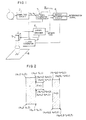
- Fig. 1 shows in block diagram a mask pattern checking system to which the present invention is applicable.
- the system comprises a memory 1 having stored design data, a computing circuit 2, a bit pattern generator 3, a defect determination circuit 4, a pattern detecting sensor 5, a binary encoder 6, a clock generator 7, and a mask 8 under test.
- the bit pattern generator 3 generates reference patterns in synchronism with the output from the pattern detecting sensor 5 on the basis of the start point and end point addresses X s1 , X s1 ; X s2 , X e2 ; ...; X sm , X em on the pattern existing coordinate j for each scanning line which addresses are produced by the calculation from apex coordinate data each pattern stored in the memory 1, as shown in Fig. 2.
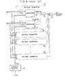
- the conventional form of the bit pattern generator 3 comprises a number of pattern generators circuits 3 1 -3 n which suffices for coordinate data X s1 , X e1 ; X s2 , X e2 : ...; X sm , X em .
- Each pattern generator circuit includes latch circuits 10 and 11 for X s and X e , comparators 12 and 13 for comparing latched data with the count X ck of a scanning address counter 15, and an AND gate 14 for producing a logical product between the outputs of the comparators 12 and 13.
- the bit pattern output from each of the generator circuits 3 1 -3 n are generated through an OR gate 16 on a real time basis in synchronism with the scanning clock signal.
- An object of the present invention as set forth in claim 1 is to provide a bit pattern generator in which the above problems are eliminated and which can generate bit patterns, stably and at high speed, for a high density mask pattern.
- two RAM memories are provided for storing a bit pattern for a scanning line produced from design data.
- a bit pattern is created and stored in one of the memories, the previously created and stored bit pattern is read out from the other memory.
- a scanning line is divided into a plurality of bytes.
- Model patterns of bit patterns existing in the respective bytes are stored in a ROM. From the combination of start point and end point addresses specifying the byte positions and the ROM addresses, a ROM address for each byte is logically determined so that any model patterns in the ROM are sequentially stored in the first mentioned memories.
- binary bit patterns are created in the following processes.
- a number of bits included in a single scanning line are divided into bytes having a fixed bit length and logical operations are sequentially performed for each byte.
- X s1 and X e1 By the comparison with X s1 and X e1 , one of model patterns preliminarily stored in byte units in a ROM is selectively read out, and the selected model pattern is stored in a bit pattern creating memory. This procedure is carried out for all bytes, and the creation of a bit pattern for one of the data X s1 and X e1 is completed.
- bit pattern data in a byte unit for X S2 and X e2 is generated and stored in the bit pattern creating memory while taking a logical sum with the previously stored bit pattern.
- bit patterns for X s3 , X e3 ; ... ; X sn , X en are sequentially stored to complete bit patterns for the entire single scanning line.
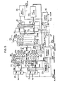
- Fig. 5 is a block diagram showing a bit pattern generator according to an embodiment of the present invention.
- a scanning line is composed of 1024 bits of picture elements, 16 bits form one byte and 64 bytes of bit patterns are generated.
- a bit pattern of 1024 bits for a single scanning line as shown in Fig. 6A is divided into bit patterns of 16 bits by 64 bytes as shown in Fig. 6B.
- Any bit among 1024 bits can be specified by designating a byte position or one of the divided positions 0-63 (hereinafter referred to byte address X CNT ) and a bit position within that byte (hereinafter referred to as bit address). This may be achieved, for example, by designating start point and end point addresses X s and X. of a pattern in respective 10-bit binary numbers each of which includes higher or upper 6 bits assigned to a byte address X SH (or X eH ) and lower 4 bits assigned to a bit address X sL (or X eL .
- Reference numeral 21 denotes a latch circuit for holding the above-mentioned 10-bit start point address X s (byte address X sH and bit address X sL ), and numeral 22 is a latch circuit for holding the 10-bit end point address X e (byte address X eH and bit address Xed.
- Numeral 23 is an address counter for counting the byte address.
- Numeral 24 is a comparator for comparing the byte address X eH in the latch circuit 22 with the count of the address counter 23, and numeral 25 is a comparator for comparing the byte address X sH in the latch circuit 21 with the count of the address counter 23.
- Numeral 26 is an end point/start point bit address calculator which generates address signals A H and A L for a ROM 27 based on the bit address X eL in the latch circuit 22 and the bit address X sL in the latch circuit 21.
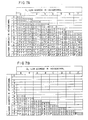
- 16-bit model patterns as shown in Figs. 7A and 7B are stored in the ROM 27. Any model pattern is read out from the ROM 27 in accordance with the address signals A H and A L .
- Numeral 28 is a sequence control circuit which provides a latch command signal to the latch circuits 21 and 22, a counter clock signal to the address counter 23, a "0" or "1" data production command to a gate circuit 29, switching signals to four switching circuits 32, 33, 37 and 38, and an X CNT signal to RAMs 30 and 31.
- Each of the switching circuits 32 and 33 is changed over for every scanning line in response to the switching signal sequence control circuit 28.
- Numeral 34 is a bit latch circuit which contributes to the pattern creation to feed back, data of the RAM 31 (or 30) supplied through the switching circuit 33, to the gate circuit 29.
- Numeral 35 is a shift register which receives data of the RAM 30 (or 31) through the switching circuit 32 in a parallel (e.g. bit- parallel) fashion and outputs the data in a serial fashion.
- Numeral 36 is an output control circuit for supplying a clock signal to the shift register 35.
- the switching circuit 37 is changed over by the sequence control circuit 28 and it controls the (writing or reading) operations of the RAMs 30 and 31.
- the switching circuit 37 provides the byte address X CNT for the RAM in a writing mode.
- the switching circuit 38 is changed over by the sequence control circuit 28 and supplies the clock from the output control circuit 36 to the RAM in a reading mode.
- the writing and reading operations of the paired RAMs 30 and 31 are controlled for every scanning line.
- the switch positions in the four switching circuits 32, 33, 37 and 38 shown in Fig. 5 indicate the case where the RAM 30 is in a reading mode while the RAM 31 is in a writing mode. Accordingly, the RAM 30 is controlled for reading by the clock 36a supplied from the output control circuit 36 through the switching circuit 38 to provide the RAM output 30a to the shift register 35 through the switching circuit 32.
- the RAM 31 is controlled for writing by the output 28e from the sequence control circuit 28 through the switching circuit 37 to supply a part of the created pattern through the switching circuit 33 to the bit latch circuit 34. The following will describe primarily the writing of data in the RAM 31.
- a scanning line of 1024 bits is divided into 64 bytes for generating a bit pattern. Accordingly, there are three forms in which the start point and end point addresses X s and X e on a scanning line, as shown in Fig. 8.
- a first form is the case where .both X s and X e exist within a single byte address, as shown by a pattern P 1 .
- a second form is the case where X s and X e exist over two adjacent byte addresses, as shown by a pattern P 2 .
- a third form is the case where X s and X. exist over three or more byte addresses, as shown by a pattern P 3 . Description of bit pattern generation will proceed following the three cases.
- the creation of pattern data starts by supplying the "0" data production command 28d from the sequence control circuit 28 to sixteen AND gates 29b1-29b16 in the gate circuit 29 so that all bits of the RAM 31 are reset to "0"s.
- the present invention is based on the convention that all bits of the RAM 31 are initially reset to “0”s and portions where patterns are shown in Fig. 8 exist are then set to "1"s. This intends to reduce a time for logical operation, since it is obvious that bit patterns are included only in bytes between X sH and X eH and hence it is only required that the generation of bit patterns is made for bytes in the range of X sH ⁇ X CNT ⁇ X eH .
- the start point and end point addresses of the three patterns P 1 , P 2 and P 3 on a scanning line L 1 shown in Fig. 8 are termed X s1 , X e1 ; X s2 , X e2 ; and X s3 , X e3 , respectively, and they are given in 10-bit binary numbers as follows: In the parentheses are shown the byte and bit addresses X sH and X sL or X eH and X eL for each start point or end point address X s or X e in 64's and hexadecimal notations.
- the start point and end point addresses X s1 and X e1 of the pattern P 1 are inputted to the respective latch circuits 21 and 22 by the latch command signal 28a issued from the sequence control circuit 28.
- the latch circuit 21 sends the higher 6 bits X SH of X s1 , which will be a logical operation starting byte address, to the byte address counter 23 which controls or supervises a byte address at which the logical operation is being performed.
- the output X CNT of the address counter 23 is fed through the sequence control circuit 28 and the switching circuit 37 to the RAM 31 to designate the location of writing therein.
- the ROM 27 has preliminarily stored 16-bit model patterns as shown in Figs. 7A and 7B, and the contents of the ROM 27 corresponding to the address signals are read out and delivered as a 16-bit pattern.
- the output 24b is in a high level.
- Second inputs of the OR gates 26a-26d are applied with the bit address X e1L of the end point address X e1 from the latch circuit 22.
- these OR gates provide "C" (hexadecimal) as the address signal A H .
- bit pattern P 2 which is shared by two bytes as shown in Fig. 8.
- the address counter provides its output X CNT being X s2H held in the latch circuit 21, thereby designating the writing location of the RAM 31 through the sequence control circuit 28 and the switching circuit 37 in the same manner as mentioned previously.
- bit pattern P 3 in Fig. 8 will be described.
- the present embodiment considers a fact that the condition of X SH ⁇ X CNT can be detected from a high level in the output 25b of the comparator 25 and the condition of X CNT ⁇ X eH can be detected from a high level in the output 24a of the comparator 24 or a low level in output 24b thereof (i.e., the absence of an END signal) due to the nature of the end point address X e .
- the sequence control circuit 28 issues on its output 28c a "1" data production command to the OR gates 29a1-29a16 in the gate circuit 29 when the circuit 28 detects a high level in the comparator output 25b and a low level in the comparator output 24b. This operation is repeated while incrementing the address counter 23, whereby a time for logical operations in the gate circuit 26 and a time for access to the ROM 27 can be saved.
- bit patterns are stored in the entire area of the RAM 31.
- Fig. 8 the patterns P 1 , P 2 and P 3 are separated from each other, there can exist a pattern P 4 , as shown by the double-dot and dash line in Fig. 8, which partly overlaps on another pattern (P 2 ).
- the present embodiment is further provided with the bit latch circuit 34.
- the output control circuit 36 operates so that the RAM (30 or 31 selected for output) transfers the created 16-bit bit pattern to the shift register 35 which in turn delivers the bit pattern in a bit-serial fashion in response to the external clock.
- the present invention allows the real time generation of bit patterns for a high density mask pattern at high speed while employing a simple circuit arrangement including the RAM 27 of a small capacity resulting in the achievement of higher economy, higher processing speed and higher stability of performance as compared with prior art generator.
Description
- The present invention relates to a mask pattern checking system in which the presence or absence of pattern defects on a mask used for the exposure of patterns on wafers in fabricating semiconductor devices such as ICs and LSIs is checked through comparison with design data. The invention particularly relates to bit pattern generator in such a system for automatically generating bit patterns based on the design data.
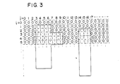
- Fig. 1 shows in block diagram a mask pattern checking system to which the present invention is applicable. The system comprises a
memory 1 having stored design data, acomputing circuit 2, abit pattern generator 3, adefect determination circuit 4, apattern detecting sensor 5, abinary encoder 6, aclock generator 7, and amask 8 under test. Thebinary encoder 6 receives the output of thepattern detecting sensor 5 to provide binary data in the sequence of i=0; j=0, 1, 2, ..., n: i=1; j=0, 1, 2, ..., n: ... corresponding to the mask pattern image scanned by thepattern detecting sensor 5 as exemplified in Fig. 3. Thebit pattern generator 3 generates reference patterns in synchronism with the output from thepattern detecting sensor 5 on the basis of the start point and end point addresses Xs1, Xs1; Xs2, Xe2; ...; Xsm, Xem on the pattern existing coordinate j for each scanning line which addresses are produced by the calculation from apex coordinate data each pattern stored in thememory 1, as shown in Fig. 2. - As shown in Fig. 4, the conventional form of the
bit pattern generator 3 comprises a number of pattern generators circuits 31-3n which suffices for coordinate data Xs1, Xe1; Xs2, Xe2: ...; Xsm, Xem. Each pattern generator circuit includeslatch circuits comparators scanning address counter 15, and anAND gate 14 for producing a logical product between the outputs of thecomparators OR gate 16 on a real time basis in synchronism with the scanning clock signal. - However, as the integration of semiconductor devices has advanced much higher recently, the number of data X. and Xe to be processed by the bit pattern generator increases, resulting in a complex circuit arrangement including a large number (200-300 sets or more) of pattern generator circuits 31-3n. This also requires long wiring, causing problems of signal propagation time, and it is difficult to generate bit patterns at high speed in syncronism with the pattern detecting sensor.
- An object of the present invention as set forth in
claim 1 is to provide a bit pattern generator in which the above problems are eliminated and which can generate bit patterns, stably and at high speed, for a high density mask pattern. - In the present invention, two RAM memories are provided for storing a bit pattern for a scanning line produced from design data. When a bit pattern is created and stored in one of the memories, the previously created and stored bit pattern is read out from the other memory. For the creation of each bit pattern, a scanning line is divided into a plurality of bytes. Model patterns of bit patterns existing in the respective bytes are stored in a ROM. From the combination of start point and end point addresses specifying the byte positions and the ROM addresses, a ROM address for each byte is logically determined so that any model patterns in the ROM are sequentially stored in the first mentioned memories.
- Preferred embodiments of the invention will be described referring to the accompanying drawings, in which:
- Fig. 1 is a general block diagram of a mask pattern checking system to which the present invention is applicable;
- Fig. 2 shows an example of design data of mask patterns supplied to the mask pattern checking system ;
- Fig. 3 shows an example of binary data provided from the binary encoder shown in Fig. 1.
- Fig. 4 is a block diagram showing the conventional bit pattern generator;
- Fig. 5 is a block diagram showing a bit pattern generator according to an embodiment of the present invention;
- Figs. 6A and 6B are illustrations showing the structure of a single scanning line;
- Figs. 7A and 7B show examples of a model pattern stored in the ROM shown in Fig. 5;
- Fig. 8 shows examples of design data of preliminarily prepared patterns; and
- Figs. 9A and 9B are charts explaining the operational processes performed in the disclosed embodiment.
- In the present invention, binary bit patterns are created in the following processes. A number of bits included in a single scanning line are divided into bytes having a fixed bit length and logical operations are sequentially performed for each byte. By the comparison with Xs1 and Xe1, one of model patterns preliminarily stored in byte units in a ROM is selectively read out, and the selected model pattern is stored in a bit pattern creating memory. This procedure is carried out for all bytes, and the creation of a bit pattern for one of the data Xs1 and Xe1 is completed. Next, bit pattern data in a byte unit for XS2 and Xe2 is generated and stored in the bit pattern creating memory while taking a logical sum with the previously stored bit pattern. Similarly, bit patterns for Xs3, Xe3 ; ... ; Xsn, Xen are sequentially stored to complete bit patterns for the entire single scanning line.
- The division into bytes and the sequential logical operations for each byte are employed since the concurrent operations for all bits on a single scanning line needs a great amount of hardware although it takes a short total processing time. By reducing the number of bits constituting a byte as small as possible in consideration of the processing speed required for the system, hardware can be simplified, which is desirable for practicing the system.
- Fig. 5 is a block diagram showing a bit pattern generator according to an embodiment of the present invention. In this embodiment, a scanning line is composed of 1024 bits of picture elements, 16 bits form one byte and 64 bytes of bit patterns are generated. A bit pattern of 1024 bits for a single scanning line as shown in Fig. 6A is divided into bit patterns of 16 bits by 64 bytes as shown in Fig. 6B. Any bit among 1024 bits can be specified by designating a byte position or one of the divided positions 0-63 (hereinafter referred to byte address XCNT) and a bit position within that byte (hereinafter referred to as bit address). This may be achieved, for example, by designating start point and end point addresses Xs and X. of a pattern in respective 10-bit binary numbers each of which includes higher or upper 6 bits assigned to a byte address XSH (or XeH) and lower 4 bits assigned to a bit address XsL (or XeL.
- Individual components in the bit pattern generator shown in Fig. 5 will now be described in brief.
Reference numeral 21 denotes a latch circuit for holding the above-mentioned 10-bit start point address Xs (byte address XsH and bit address XsL), andnumeral 22 is a latch circuit for holding the 10-bit end point address Xe (byte address XeH and bit address Xed. Numeral 23 is an address counter for counting the byte address. Numeral 24 is a comparator for comparing the byte address XeH in thelatch circuit 22 with the count of the address counter 23, andnumeral 25 is a comparator for comparing the byte address XsH in thelatch circuit 21 with the count of the address counter 23.Numeral 26 is an end point/start point bit address calculator which generates address signals AH and AL for aROM 27 based on the bit address XeL in thelatch circuit 22 and the bit address XsL in thelatch circuit 21. 16-bit model patterns as shown in Figs. 7A and 7B are stored in theROM 27. Any model pattern is read out from theROM 27 in accordance with the address signals AH and AL. Numeral 28 is a sequence control circuit which provides a latch command signal to thelatch circuits gate circuit 29, switching signals to fourswitching circuits RAMs 30 and 31. Each of theRAMs 30 and 31 has a capacity of one scanning line (16 bitsx64 bytes=1024 bits). Each of theswitching circuits switching circuit 33, to thegate circuit 29.Numeral 35 is a shift register which receives data of the RAM 30 (or 31) through theswitching circuit 32 in a parallel (e.g. bit- parallel) fashion and outputs the data in a serial fashion.Numeral 36 is an output control circuit for supplying a clock signal to theshift register 35. Theswitching circuit 37 is changed over by the sequence control circuit 28 and it controls the (writing or reading) operations of theRAMs 30 and 31. Theswitching circuit 37 provides the byte address XCNT for the RAM in a writing mode. Theswitching circuit 38 is changed over by the sequence control circuit 28 and supplies the clock from theoutput control circuit 36 to the RAM in a reading mode. - In operation, the writing and reading operations of the paired
RAMs 30 and 31 are controlled for every scanning line. The switch positions in the fourswitching circuits RAM 30 is in a reading mode while the RAM 31 is in a writing mode. Accordingly, theRAM 30 is controlled for reading by the clock 36a supplied from theoutput control circuit 36 through the switchingcircuit 38 to provide theRAM output 30a to theshift register 35 through the switchingcircuit 32. On the other hand, the RAM 31 is controlled for writing by the output 28e from the sequence control circuit 28 through the switchingcircuit 37 to supply a part of the created pattern through the switchingcircuit 33 to the bit latch circuit 34. The following will describe primarily the writing of data in the RAM 31. - As mentioned previously, a scanning line of 1024 bits is divided into 64 bytes for generating a bit pattern. Accordingly, there are three forms in which the start point and end point addresses Xs and Xe on a scanning line, as shown in Fig. 8. A first form is the case where .both Xs and Xe exist within a single byte address, as shown by a pattern P1. A second form is the case where Xs and Xe exist over two adjacent byte addresses, as shown by a pattern P2. A third form is the case where Xs and X. exist over three or more byte addresses, as shown by a pattern P3. Description of bit pattern generation will proceed following the three cases.
- The creation of pattern data starts by supplying the "0"
data production command 28d from the sequence control circuit 28 to sixteen AND gates 29b1-29b16 in thegate circuit 29 so that all bits of the RAM 31 are reset to "0"s. The present invention is based on the convention that all bits of the RAM 31 are initially reset to "0"s and portions where patterns are shown in Fig. 8 exist are then set to "1"s. This intends to reduce a time for logical operation, since it is obvious that bit patterns are included only in bytes between XsH and XeH and hence it is only required that the generation of bit patterns is made for bytes in the range of XsH≦XCNT≦XeH. - The start point and end point addresses of the three patterns P1, P2 and P3 on a scanning line L1 shown in Fig. 8 are termed Xs1, Xe1; Xs2, Xe2; and Xs3, Xe3, respectively, and they are given in 10-bit binary numbers as follows:


- After all bits of the RAM 31 have been initialy reset to "0"s, as mentioned above, the start point and end point addresses Xs1 and Xe1 of the pattern P1 are inputted to the
respective latch circuits latch command signal 28a issued from the sequence control circuit 28. Thelatch circuit 21 sends the higher 6 bits XSH of Xs1, which will be a logical operation starting byte address, to the byte address counter 23 which controls or supervises a byte address at which the logical operation is being performed. The output XCNT of the address counter 23 is fed through the sequence control circuit 28 and the switchingcircuit 37 to the RAM 31 to designate the location of writing therein. The XCNT is also delivered to thecomparators bit address calculator 26 as address signals for theROM 27 from which a necessary pattern is in turn generated. TheROM 27 has preliminarily stored 16-bit model patterns as shown in Figs. 7A and 7B, and the contents of theROM 27 corresponding to the address signals are read out and delivered as a 16-bit pattern. - Explanation will now be made of the results of comparison by the
comparators bit address calculator 26. In thecomparator 25, XCNT=XS1H is satisfied so that the output 25a being a high level is applied to first inputs of four ANDgates 26e-26h. Second inputs of the ANDgates 26e-26h are applied with the bit address Xs1L of the start point address Xs1 from thelatch circuit 21. As a result, these AND gates provide "4" (hexadecimal) as the address signal AL. On the other hand, in thecomparator 24, XCNT=Xe1H is satisfied so thattheoutput 24a being a low level is applied to first inputs of four ORgates 26a-26d. Theoutput 24b is in a high level. Second inputs of theOR gates 26a-26d are applied with the bit address Xe1L of the end point address Xe1 from thelatch circuit 22. As a result, these OR gates provide "C" (hexadecimal) as the address signal AH. - The address signals AL (=4) and AH (=C) for the
ROM 27 are thus calculated and a model bit pattern of "1FFO" shown in Fig. 9A is read out from theROM 27. This bit pattern is delivered to the RAM 31 through thegate circuit 29 including sixteen OR gates 29a1-29a16 and sixteen AND gates 29b1-29b16, and stored in a location thereof specified by XCNT=1. Since the inputs of the AND gates 29b1-29b16 connected to from the sequence control circuit 28 are rendered to low levels after the initial "0" data has been created, the output of theROM 27 can pass through these AND gates. - The
output 24b of thecomparator 24 takes a high level when XCNT=Xe1H, as mentioned above, and thisoutput 24b is applied to the sequence control circuit 28 as an END signal indicating the termination of a logical operation specified by Xs1 and Xe1' Upon receipt of the END signal, the sequence control circuit 28 issues alatch command signal 28a so that thelatch circuits - The following will describe the generation of bit pattern P2 which is shared by two bytes as shown in Fig. 8. First, the address counter provides its output XCNT being Xs2H held in the
latch circuit 21, thereby designating the writing location of the RAM 31 through the sequence control circuit 28 and the switchingcircuit 37 in the same manner as mentioned previously. In thecomparator 25, XCNT=Xs2H is satisfied so that the output 25a takes a high level. Therefore, the ANDgates 26e-26h provide the address signal AL="4" (hexadecimal) in accordance with the bit address Xs2L of the start point address Xs2. On the other hand, a relation between the byte address Xe2H ("3" in 64's notation) of the end point address Xe2 and the XCNT ("2" in 64's notation) of the address counter 23 in thecomparator 24 is as follows:
output 24a of thecomparator 24 takes a high level so that the ORgates 26a-26d having the first inputs connected to thecomparator output 24a provide an output AH="F" (hexadecimal) irrespective of the second inputs thereof. As a result, the address signals AL=4 and AH=F are fed to theROM 27 from which a model pattern of "FFFO" in the pattern table shown in Fig. 7A or a pattern shown on the left side of Fig. 9B is in turn read out. This pattern is delivered through thegate circuit 29 to the RAM 31 and stored in a location thereof designated byX CNT =2. - In the previous description for the generating of the pattern P1, it has been mentioned that the logical operation specified by the start point and end point addresses Xs and Xe terminates when a condition of XeH=XCNT is met. However, the logical operation will proceed if that condition is not met, and the sequence control circuit 28 produces a
counter clock 28b by detecting, for example, the absence of an END signal so that thebyte address counter 25 is incremented. Now, the address counter 23 provides XCNT=3. Therefore, the writing location of the RAM 31 is correspondingly changed. - In the
comparator 25, a relation between the byte address Xs2H ("2" in 64's notation) of the start point address XS2 and the XCNT (=3) of the address counter 23 is as follows:
comparator 25 takes a low level so that the ANDgates 26e-26h having the first inputs connected to the comparator output 25a provide an output AL=0 (hexadecimal) irrespective of the second inputs thereof. On the other hand in thecomparator 25, Xe2H=XCNT=3 is satisfied so that theoutput 24a takes a low level. Therefore, the ORgates 26a-26d provide an address signal AH="4" (hexadecimal) in accordance with the bit address Xe2L of the end point address Xe2. As a result, the address signals AL=0 and AH=4 are fed to theROM 27 from which a model pattern of "001 F" in the pattern table shown in Fig. 7A or a pattern shown on the right side of Fig. 9B is in turn read out. This pattern is delivered through thegate circuit 29 to the RAM 31 and stored in a location thereof designated by XCNT=3. - The
comparator 24 satisfies Xe2H=XCNT=3, providing at itsoutput 24b an END signal to the sequence control circuit 28. Then, logical operations are turned to the subsequent patterns P3, P4,.... - Finally, the generation of bit pattern P3 in Fig. 8 will be described. In this case, logical operations for portions XCNT=4 and XcNT=7 are the same as those for XCNT=2 and XCNT=3. Therefore, explanation thereof will be omitted.
- For the generation of pattern P3, it is noted that conditions of

comparators bit address calculator 26. This is because the output 25a of thecomparator 25 takes a low level to make an address signal AL=0 and theoutput 24a of thecomparator 24 takes a high level to make an address signal AH=F, thereby providing a model pattern of "FFFF" as shown in Fig. 7A. However, it is undesirably a waste of computation time to access theROM 27 each time when XsH<XCNT<XeH is met, notwithstanding that theROM 27 always provides a model pattern of "FFFF" in such cases. The longer the pattern P3 as shown in Fig. 8 in the lateral direction, the longer will be the waste time. The present embodiment considers a fact that the condition of XSH<XCNT can be detected from a high level in theoutput 25b of thecomparator 25 and the condition of XCNT<XeH can be detected from a high level in theoutput 24a of thecomparator 24 or a low level inoutput 24b thereof (i.e., the absence of an END signal) due to the nature of the end point address Xe. Then, the sequence control circuit 28 issues on its output 28c a "1" data production command to the OR gates 29a1-29a16 in thegate circuit 29 when the circuit 28 detects a high level in thecomparator output 25b and a low level in thecomparator output 24b. This operation is repeated while incrementing the address counter 23, whereby a time for logical operations in thegate circuit 26 and a time for access to theROM 27 can be saved. - With the foregoing operations, bit patterns are stored in the entire area of the RAM 31.
- Although in Fig. 8 the patterns P1, P2 and P3 are separated from each other, there can exist a pattern P4, as shown by the double-dot and dash line in Fig. 8, which partly overlaps on another pattern (P2). In consideration of such a case, the present embodiment is further provided with the bit latch circuit 34.
- A portion of the pattern P2 on a scanning line L2 is stored in locations in the RAM corresponding to XCNT=2 and XCNT=3, in the same manner as mentioned previously. In storing the pattern P4 in the location of XCNT=3 in the RAM, data previously stored in the XCNT=3 is once retrieved to the latch circuit 34, a logical sum thereof with the ROM contents is produced by the OR gates 29a1-29a16, and then the result is stored in the same RAM location. This procedure allows not only twofold patterns but patterns of threefold or more can also be treated.
- Thus, the storing of data to one (RAM 31 in the explained example) of the
RAMs 30 and 31 is completed. While a bit pattern is created in the RAM 31, theRAM 30 outputs a bit pattern which has been created. In the next scanning period, the RAM 31 outputs the created bit pattern while a bit pattern is created and stored in theRAM 30. These repetitive operations are switched by the switchingcircuits - In outputting the bit patterns, the
output control circuit 36 operates so that the RAM (30 or 31 selected for output) transfers the created 16-bit bit pattern to theshift register 35 which in turn delivers the bit pattern in a bit-serial fashion in response to the external clock. - As described above, the present invention allows the real time generation of bit patterns for a high density mask pattern at high speed while employing a simple circuit arrangement including the
RAM 27 of a small capacity resulting in the achievement of higher economy, higher processing speed and higher stability of performance as compared with prior art generator. - It should be noted that blank portions of the tables in Figs. 7A and 7B are unused portions of the memory, and the memory contents are expressed in hexadecimal notation. Addresses A, B, C, D, E and F are 10, 11, 12, 13, 14 and 15 in decimal.
Claims (6)
Applications Claiming Priority (2)
| Application Number | Priority Date | Filing Date | Title |
|---|---|---|---|
| JP160173/81 | 1981-10-09 | ||
| JP56160173A JPS5861629A (en) | 1981-10-09 | 1981-10-09 | Bit pattern generator |
Publications (3)
| Publication Number | Publication Date |
|---|---|
| EP0077045A2 EP0077045A2 (en) | 1983-04-20 |
| EP0077045A3 EP0077045A3 (en) | 1986-01-29 |
| EP0077045B1 true EP0077045B1 (en) | 1988-08-03 |
Family
ID=15709423
Family Applications (1)
| Application Number | Title | Priority Date | Filing Date |
|---|---|---|---|
| EP82109329A Expired EP0077045B1 (en) | 1981-10-09 | 1982-10-08 | Bit pattern generator |
Country Status (4)
| Country | Link |
|---|---|
| US (1) | US4528634A (en) |
| EP (1) | EP0077045B1 (en) |
| JP (1) | JPS5861629A (en) |
| DE (1) | DE3278862D1 (en) |
Families Citing this family (16)
| Publication number | Priority date | Publication date | Assignee | Title |
|---|---|---|---|---|
| JPS60143704A (en) * | 1983-12-29 | 1985-07-30 | Nippon Jido Seigyo Kk | Defect inspecting method of pattern |
| JPH0641966B2 (en) * | 1984-02-15 | 1994-06-01 | 株式会社アドバンテスト | Pattern generator |
| EP0186874B1 (en) * | 1984-12-26 | 1994-06-08 | Hitachi, Ltd. | Method of and apparatus for checking geometry of multi-layer patterns for IC structures |
| JPS61265521A (en) * | 1985-05-20 | 1986-11-25 | Meteoola Syst Kk | Apparatus for automatically measuring shape of figure |
| JP2569303B2 (en) * | 1985-07-05 | 1997-01-08 | 日本電装株式会社 | Image processing apparatus for performing cumulative addition of image data |
| US5142621A (en) * | 1985-12-03 | 1992-08-25 | Texas Instruments Incorporated | Graphics processing apparatus having instruction which operates separately on X and Y coordinates of pixel location registers |
| US4837447A (en) * | 1986-05-06 | 1989-06-06 | Research Triangle Institute, Inc. | Rasterization system for converting polygonal pattern data into a bit-map |
| JPH0622195B2 (en) * | 1987-02-26 | 1994-03-23 | 東芝機械株式会社 | Charged beam drawing device |
| JP2810660B2 (en) * | 1987-03-06 | 1998-10-15 | 株式会社日立製作所 | Particle image analyzer |
| US5348558A (en) * | 1992-04-23 | 1994-09-20 | Mitsubishi Denki Kabushiki Kaisha | Layout pattern generating apparatus |
| US5541942A (en) * | 1994-06-14 | 1996-07-30 | Microsoft Corporation | Method and system for testing memory utilizing specific bit patterns |
| US6216224B1 (en) | 1998-06-05 | 2001-04-10 | Micron Technology Inc. | Method for read only memory shadowing |
| US6330667B1 (en) * | 1998-06-05 | 2001-12-11 | Micron Technology, Inc. | System for read only memory shadowing circuit for copying a quantity of rom data to the ram prior to initialization of the computer system |
| JP4435915B2 (en) * | 1999-11-26 | 2010-03-24 | 株式会社アドバンテスト | Pattern generation method, pattern generator, memory test equipment |
| US20050083095A1 (en) * | 2003-10-16 | 2005-04-21 | Tsvika Kurts | Adaptive input/output buffer and methods thereof |
| JP2008501126A (en) * | 2004-05-25 | 2008-01-17 | 新世代株式会社 | Data processing device, drawing device, and pixel packer |
Family Cites Families (7)
| Publication number | Priority date | Publication date | Assignee | Title |
|---|---|---|---|---|
| US3781829A (en) * | 1972-06-16 | 1973-12-25 | Ibm | Test pattern generator |
| US3891982A (en) * | 1973-05-23 | 1975-06-24 | Adage Inc | Computer display terminal |
| US4218142A (en) * | 1978-03-08 | 1980-08-19 | Aerodyne Research, Inc. | Mask analysis |
| US4280186A (en) * | 1978-07-07 | 1981-07-21 | Tokyo Shibaura Denki Kabushiki Kaisha | Exposure apparatus using electron beams |
| US4377849A (en) * | 1980-12-29 | 1983-03-22 | International Business Machines Corporation | Macro assembler process for automated circuit design |
| US4433384A (en) * | 1981-10-05 | 1984-02-21 | Varian Associates, Inc. | Pattern data handling system for an electron beam exposure system |
| US4482810A (en) * | 1982-09-30 | 1984-11-13 | Storage Technology Partners | Electron beam exposure system |
-
1981
- 1981-10-09 JP JP56160173A patent/JPS5861629A/en active Granted
-
1982
- 1982-10-08 EP EP82109329A patent/EP0077045B1/en not_active Expired
- 1982-10-08 DE DE8282109329T patent/DE3278862D1/en not_active Expired
- 1982-10-08 US US06/433,405 patent/US4528634A/en not_active Expired - Fee Related
Also Published As
| Publication number | Publication date |
|---|---|
| EP0077045A3 (en) | 1986-01-29 |
| JPS6246036B2 (en) | 1987-09-30 |
| US4528634A (en) | 1985-07-09 |
| DE3278862D1 (en) | 1988-09-08 |
| EP0077045A2 (en) | 1983-04-20 |
| JPS5861629A (en) | 1983-04-12 |
Similar Documents
| Publication | Publication Date | Title |
|---|---|---|
| EP0077045B1 (en) | Bit pattern generator | |
| US5097442A (en) | Programmable depth first-in, first-out memory | |
| JPH065513B2 (en) | Memory system | |
| JPS6234133B2 (en) | ||
| US4621360A (en) | Control method of data transfer | |
| US4805173A (en) | Error control method and apparatus | |
| KR930009077A (en) | Layout element layout design system | |
| GB2154348A (en) | Bit pattern conversion apparatus | |
| US4839826A (en) | Affine conversion apparatus using a raster generator to reduce cycle time | |
| US5577182A (en) | Image processing apparatus | |
| US4222339A (en) | Automatic compound pattern generation type sewing machine | |
| JPH0231417B2 (en) | ||
| US6108803A (en) | Memory cell circuit for executing specific tests on memory cells that have been designated by address data | |
| KR910004262B1 (en) | Memory device having address control function | |
| JPS6249570A (en) | Picture processor | |
| JPH02108171A (en) | Frame memory device | |
| JPS6019258A (en) | Memory | |
| JPH0668243A (en) | Image input device | |
| JP2893915B2 (en) | Semiconductor integrated circuit with built-in memory | |
| JP3099774B2 (en) | Semiconductor integrated circuit | |
| JP2552287B2 (en) | System bus method | |
| JPH0112309Y2 (en) | ||
| JPH0222422B2 (en) | ||
| JPS63311182A (en) | Test pattern memory circuit | |
| JPS6011398B2 (en) | Memory test pattern writing device |
Legal Events
| Date | Code | Title | Description |
|---|---|---|---|
| PUAI | Public reference made under article 153(3) epc to a published international application that has entered the european phase |
Free format text: ORIGINAL CODE: 0009012 |
|
| AK | Designated contracting states |
Designated state(s): DE FR GB |
|
| 17P | Request for examination filed |
Effective date: 19830609 |
|
| PUAL | Search report despatched |
Free format text: ORIGINAL CODE: 0009013 |
|
| RHK1 | Main classification (correction) |
Ipc: G06F 1/02 |
|
| AK | Designated contracting states |
Designated state(s): DE FR GB |
|
| 17Q | First examination report despatched |
Effective date: 19870820 |
|
| GRAA | (expected) grant |
Free format text: ORIGINAL CODE: 0009210 |
|
| AK | Designated contracting states |
Kind code of ref document: B1 Designated state(s): DE FR GB |
|
| REF | Corresponds to: |
Ref document number: 3278862 Country of ref document: DE Date of ref document: 19880908 |
|
| ET | Fr: translation filed | ||
| PLBE | No opposition filed within time limit |
Free format text: ORIGINAL CODE: 0009261 |
|
| STAA | Information on the status of an ep patent application or granted ep patent |
Free format text: STATUS: NO OPPOSITION FILED WITHIN TIME LIMIT |
|
| 26N | No opposition filed | ||
| PGFP | Annual fee paid to national office [announced via postgrant information from national office to epo] |
Ref country code: GB Payment date: 19910808 Year of fee payment: 10 |
|
| PGFP | Annual fee paid to national office [announced via postgrant information from national office to epo] |
Ref country code: FR Payment date: 19910918 Year of fee payment: 10 |
|
| PGFP | Annual fee paid to national office [announced via postgrant information from national office to epo] |
Ref country code: DE Payment date: 19911127 Year of fee payment: 10 |
|
| PG25 | Lapsed in a contracting state [announced via postgrant information from national office to epo] |
Ref country code: GB Effective date: 19921008 |
|
| GBPC | Gb: european patent ceased through non-payment of renewal fee |
Effective date: 19921008 |
|
| PG25 | Lapsed in a contracting state [announced via postgrant information from national office to epo] |
Ref country code: FR Effective date: 19930630 |
|
| PG25 | Lapsed in a contracting state [announced via postgrant information from national office to epo] |
Ref country code: DE Effective date: 19930701 |
|
| REG | Reference to a national code |
Ref country code: FR Ref legal event code: ST |