EP0076832B1 - Sense amplifier comparator circuit - Google Patents
Sense amplifier comparator circuit Download PDFInfo
- Publication number
- EP0076832B1 EP0076832B1 EP82901273A EP82901273A EP0076832B1 EP 0076832 B1 EP0076832 B1 EP 0076832B1 EP 82901273 A EP82901273 A EP 82901273A EP 82901273 A EP82901273 A EP 82901273A EP 0076832 B1 EP0076832 B1 EP 0076832B1
- Authority
- EP
- European Patent Office
- Prior art keywords
- comparator circuit
- circuit
- path
- amplification
- mode
- Prior art date
- Legal status (The legal status is an assumption and is not a legal conclusion. Google has not performed a legal analysis and makes no representation as to the accuracy of the status listed.)
- Expired
Links
Images

Classifications
-
- G—PHYSICS
- G11—INFORMATION STORAGE
- G11C—STATIC STORES
- G11C7/00—Arrangements for writing information into, or reading information out from, a digital store
- G11C7/06—Sense amplifiers; Associated circuits, e.g. timing or triggering circuits
- G11C7/065—Differential amplifiers of latching type
-
- H—ELECTRICITY
- H03—ELECTRONIC CIRCUITRY
- H03K—PULSE TECHNIQUE
- H03K3/00—Circuits for generating electric pulses; Monostable, bistable or multistable circuits
- H03K3/02—Generators characterised by the type of circuit or by the means used for producing pulses
- H03K3/353—Generators characterised by the type of circuit or by the means used for producing pulses by the use, as active elements, of field-effect transistors with internal or external positive feedback
- H03K3/356—Bistable circuits
Definitions
- This invention relates to comparator circuits of the kind including: a multivibrator of substantially symmetric organization having first and second conductive paths, each path containing a series connected load element and an amplification element joined through an intermediate node; coupling means adapted to selectively couple said node in said first path with said amplification element in said second path and to selectively couple said node in said second path with said amplification element in said first path; input means adapted to selectively apply first and second input signals to said amplification elements in said first and second paths; and control means connected to said coupling means and to said input means and arranged in operation to disable said coupling means concurrently with an enabling of said input means and to enable said coupling means in timed sequence thereafter.
- Such comparator circuits find application as sense amplifiers for memory arrays.
- This invention also relates to a method of operating a comparator circuit.
- Generally recognized techniques of storing data in memory arrays provide for one data bit per memory cell.
- the information in each cell is detected externally as a voltage having either a zero level or a high level, respectively corresponding to the binary states of 0 and 1. Effects such as time, temperature, and read-write cycling of the memory array, tend to degrade the window between the voltages associated with each of the two binary states. For these and numerous other reasons, little prior effort has been directed toward subdividing the voltage window and thereby increasing the data stored in each cell.
- each memory cell stores two binary bits of information, and requires memory output signals at four distinct voltage levels to distinguish therebetween.
- each of the binary states (00, 01, 10, and 11) corresponds to a substantially equal segment of the voltage window between the outer bounds of ground potential and the power supply.
- each such circuit must compare the memory voltage read from the array with a segmented level of the operating window to determine which is greater.
- the comparator circuits otherwise known as sense amplifiers, must have a short settling time. Specifically, distinguishing between voltages in the manner suggested does not appear particularly onerous. However, the difficulties begin to take form when one recognizes some fundamental constraints. For instance, since the output data must be binary in form, each sense amplifier circuit must latch or otherwise select either extreme of the two binary format output states. Furthermore, the sense amplifier must exhibit adequate differential gain to distinguish relatively small voltage differences between two relatively large voltages. No less important is the pursuit of good common mode rejection and fabrication with minimum device count or chip area.
- the input stage field effect transistors For instance, to optimize the speed and gain characteristics of such sense amplifiers, one would normally prefer to operate the input stage field effect transistors so that the gate-to-source voltages are at or very near the threshold level of the transistor.
- the two-bit-per-cell concept requires three sense amplifier circuits, each operating at substantially different levels over the range between ground potential and the supply voltage. Consequently, the voltages provided to the input stage field effect transistors of at least two sense amplifiers will not be near their threshold voltages. Selective alteration of transistor threshold voltages during integrated circuit fabrication is not an economically practical solution.
- a comparator circuit of the kind specified is known from U.S. Patent Specification No. 3,982,140.
- the known comparator circuit has the disadvantage of an unduly limited ability to compare signal levels over a range of voltages.
- the document JP-A-54-124 665 discloses a flip-flop type sense amplifier circuit having a selectively operable cross-coupled connection. Furthermore, the flip-flop circuit is connected to earth potential via the source-drain paths of a pair of MOS transistors which are selectively operable by phased control signals applied to their gate electrodes.
- a comparator circuit of the kind specified characterized by selectively operable biasing means coupled to said amplification elements and to said control means, said control means being further arranged in operation to enable said biasing means concurrently with the enabling of said input means and to disable said biasing means concurrently with the disabling of said coupling means.
- the comparator circuit according to the invention alleviates the aforementioned disadvantage while retaining excellent speed, common mode rejection and gain characteristics. Chip area is minimized and outputs are presented as distinct binary levels.
- the comparator circuit operates in two modes, a DIFFERENTIAL MODE for high gain comparison and a LATCH MODE for a stable and fixed binary format output.
- the transitional dynamics between the DIFFERENTIAL and the LATCH MODES serve to define the latched binary state in direct correspondence to the amplified relative differences obtained during the DIFFERENTIAL MODE.
- a method of operating a comparator circuit to distinguish between two input signals of similar magnitude and generate a binary from output signal said comparator circuit including a bistable multivibrator circuit of substantially symmetric organization, which multivibrator circuit includes a pair of amplification elements, characterized by the steps of: operating the comparator circuit in a differential mode with respect to said input signals while biasing said amplification elements; and disabling the bias applied to said amplification elements in substantial time correspondence with a transition of the comparator circuit from a differential mode to a latch mode, while maintaining impedance symmetry during the dynamics of transition between the differential mode and the latch mode.
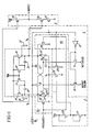
- Fig. 1 of the drawings where a representative embodiment of the circuit is schematically depicted.
- the field effect transistors are p-channel, enhancement mode MOS type integrated circuit devices.
- the capacitors shown symbolically by way of dotted lines are intrinsic gate-to-source parameters in the immediately adjacent transistors.
- supply voltage V oo is at a nominal level of -17 volts.
- Circuit section 1 enclosed within the dashed perimeter line, is very similar to the bistable multivibrator circuit disclosed in the last-noted patent.
- a push-pull operated output driver circuit, with a series connected disable transistor, is enclosed within circuit section 2.
- Circuit section 3 contains a constant current source, regulated by a voltage divider and connected in parallel with a disabling transistor.
- Bifurcated circuit sections 4a and 4b are shown to contain individual precharge transistors.
- circuit section 1 The upper region of circuit section 1 is shown to contain substantially identical booted load circuits, serving as load elements for amplifying driver transistors 12 and 13 in the two symmetrically arranged arms of the multivibrator circuit.
- the booted load circuits contain substantially identical load transistors 14 and 16 driven by transistors 17 and 18 from common supply voltage V DD .
- the booted load circuits also contain capacitive elements, 19 and 21, between the gate and source terminals of load transistors 14 and 16, respectively.
- the circuit section designated by reference numeral 2 comprises the output coupling stage, including a set of oppositely driven push-pull transistors, 24 and 26, connected in series with the disabling transistor, 27.
- the purpose of this circuit segment is twofold.
- push-pull transistors 24 and 26 form substantially identical load impedances for multivibrator nodes V 1 and V 2 , decoupling and thereby insuring that the effects of output loads will not alter the circuit dynamics during the transition between DIFFERENTIAL and LATCH MODES of the operating sequence.
- the remaining transistor, 27, is present to prevent the formation of a short circuit path from V DD to ground through transistors 24 and 26 during the DIFFERENTIAL MODE of the operation.
- the voltages at both nodes, V 1 and V 2 lie between V DD and ground, effectively placing series connected transistors 24 and 26 into full conduction.
- the node voltages are driven to opposite extremes, placing one of the two push-pull transistors into a nonconducting state and thereby avoiding a short circuit between the power supply and ground.
- the circuit segment designated by reference numeral 3 establishes a differential organization of the circuit and biases the voltage appearing at the source terminals of driver transistors 12 and 13. In this way, the voltage levels on the MEMORY COLUMN line and REFERENCE line differ from the biased source voltage V s in an amount approximating the threshold of the driver transistors.
- Fig. 2 to illustrate, if the REFERENCE voltage is at a level of -9 volts, the MEMORY COLUMN voltage is of a similar magnitude, and the threshold voltages of transistors 12 and 13 are approximately -3 volts, node V s will be approximately -6 volts during the DIFFERENTIAL MODE of operation.
- the voltage at node V s is the greater of two voltage combinations, i.e., the MEMORY COLUMN voltage less the threshold of transistor 12 or the REFERENCE voltage less the threshold of transistor 13.
- the embodying bias circuit is shown to contain transistor 28, connected between node V s and ground potential, and operated in the manner of a constant current source.
- Transistors 29 and 31 form a voltage divider which regulates the current flow through transistor 28. Consequently, transistor 28 provides not only a commensurate level of source terminal biasing, but also common mode rejection for the input signals connected to the gate terminals of driver transistors 12 and 13. No less importans the increased differential gain as perceived at nodes V, and V 2 .
- a disabling transistor 32 suitably functioning as an electrical short for constant current source transistor 28, is shown connected in electrical parallel with transistor 28.
- the gate electrode of transistor 32 is energized by an appropriate signal on the LATCH line.
- a LATCH signal shorts the constant current source and allows the output voltages at nodes V 1 and V 2 to approach the opposite extremes of the voltage supply.
- the OUTPUT signal during the LATCH MODE follows in ordered sequence, assuming a binary format suitable to prevent the shorting of push-pull output transistors 24 and 26.
- Circuit sections 4a and 4b are shown to contain transistors 33 and 34, serving to selectively connect output nodes V 1 and V 2 with ground potential.
- transistors 33 and 34 When appropriately energized with a signal on the PRECHARGE line, transistors 33 and 34 short nodes V, and V 2 to ground.
- Booted inverter capacitors 19 and 21 are thereby charged to a voltage approaching the level of Vpp minus a FET threshold. The existence of the voltage on capacitors 19 and 21 temporarily increases the gate voltage on transistors 14 and 16 at the onset of the transient period between the DIFFERENTIAL MODE and the LATCH MODE, briefly, but significantly, increasing the current through these transistors.
- the operation of the composite circuit will be considered next.
- the regenerative dynamics coupled with the circuit symmetry ensure appropriate latching in the course of the transition from the DIFFERENTIAL MODE to the LATCH MODE.
- the multivibrator circuit must operate with substantial symmetry if the nominal voltage difference between the nodes V, and V 2 is to consistently define the final binary state of the circuit.
- the embodiment in Fig. 1 contains supplemental capacitors 36 and 37, respectively connecting nodes V, and V 2 to ground potential
- the two capacitors are substantially identical in size relative to each other, yet significant in comparison to the intrinsic capacitive loads coupled to nodes V 1 and V 2 .
- the PRECHARGE MODE designated at the top of Fig. 2, corresponds to a period when a precharge command signal energizes transistors 33 and 34 to effect a grounding of nodes V, and V 2 . V s is also brought to ground potential.
- capacitors 19 and 21 are precharged through transistors 17 and 18, with the minimum duration constrained by the component time constants. Note from the voltage plots that during the PRECHARGE MODE, the signal on the LATCH line is zero, disabling the path through transistors 9, 11, 27 and 32, while enabling conduction through transistors 6 and 7.
- the plots in Fig. 2 show that the REFERENCE line signal attains -9 volts and the MEMORY COLUMN line signal attains -8.8 volts at time to. These two signals serve as the inputs to the sense amplifier circuit.
- the amplitude of the REFERENCE signal corresponds to the voltage level distinguishing between a binary 01 state and a 10 state. From this, the -8.8 volts on the MEMORY COLUMN line illustrates memory data corresponding to the binary 01 state. Proceeding with the analysis of Fig. 2, it is apparent that immediately after time to the PRECHARGE and LATCH line signals inhibit any circuit reaction to the MEMORY COLUMN and REFERENCE line signals noted.
- REFERENCE and MEMORY COLUMN signals may, as shown, coincide in time, but are not so constrained.
- the two signals may also commence individually, at points in time between events t, and t 2 shown in the plots. However, any associated DIFFERENTIAL MODE dynamics must cease before time t 2 . In like manner, either of the two signals may also terminate at any time after the onset of the LATCH MODE at time t 2 .
- the PRECHARGE line signal ceases at time t i . Since transistors 9 and 11 in the cross-coupling arms of the multivibrator continue to remain off, the circuit then assumes a differential amplifier mode of operation. Node V s shifts to approximately -6 volt by virtue of the -9 volt REFERENCE signal and 3 volt threshold of FET 13 as nodes V, and V 2 fall to -15 and -14 volts, respectively.
- the one volt differential between nodes V, and V 2 represents a voltage gain of 5 over the difference of 0.2 volts separating the MEMORY COLUMN voltage (8.8 volts) and the REFERENCE voltage (9 volts).
- the exponential shape of the voltages on nodes V 1 and V 2 immediately following time t 1 , are attributable to the capacitive loads on each of the nodes, and particularly supplemental capacitors 36 and 37.
- Time t 2 prescribes the entry into the LATCH MODE of the operating sequence. Commencement of the mode is evidenced by the presence of a LATCH line signal, culminating soon thereafter in the latching of the bistable multivibrator into one of two states. Operatively, the onset of the LATCH signal energizes transistors 9, 11, 27 and 32, as it de-energizes data entry transistors 6 and 7. In the embodiment, the voltages at nodes V s and V 2 fall to ground potential as node V 1 rises to V oo of the power supply. The push-pull output transistors, 24 and 26, follow in prescribed manner.
- the interval between the conclusion of the t 2 transient and the onset of time t 3 provides a suitable period for sampling the multivibrator output to determine which of the two input signals, REFERENCE or MEMORY COLUMN, were greater in absolute magnitude.
- -17 volts at V, and an OUTPUT line voltage of V DD indicates that the REFERENCE line signal was greater than the signal on the MEMORY COLUMN line. Therefore, the stored data must be either 00 or 01, depending on the response of the next adjacent sense amplifier in the manner taught by the previously noted U.S. Patent. Consistent with the teaching in U.S. Patent 4,192,014, the composite of the three sensor amplifiers is necessary to ascertain the exact binary state in each memory cell.
- the dynamics of the circuit at time t 2 , as well as the initial conditions on the circuit elements immediately preceding time t 2 are important in understanding the transition between the DIFFERENTIAL MODE and the LATCH MODE.
- the dominant operative considerations are symmetry in the circuit and the asymmetry in the initial conditions stored on the capacitive elements.
- analysis of the voltage levels at nodes V, and V 2 shows that the capacitively loaded nodes differ by one volt at time t 2 .
- the appearance of a LATCH line signal at that time simultaneously energizes shorting transistor 32 and cross-coupling transistors 9 and 11.
- the initial levels of conductivity in driver transistors 12 and 13 are retained by the charge stored on the intrinsic capacitors 22 and 23.
- the LATCH MODE terminates with time t 3 .
- the onset of the PRECHARGE MODE coincides with the end of the LATCH MODE. If precharging commences prior to t 3 , the sampling period would merely be shortened accordingly. Were it to commence after time t 3 , however, the circuit would temporarily revert to the DIFFERENTIAL MODE for the interim therebetween.
- the voltage plots of the embodying circuit show that the MEMORY COLUMN line and the REFERENCE line signals fall to ground potential at time t 4 . Since the entry of these signals into the circuit is controlled by a signal inverse to the LATCH line signal, coupled to transistors 6 and 7, the MEMORY COLUMN and REFERENCE signals may remain at all times without affecting circuit operation.
- the described embodiment is operatively characterized by a sequence commencing with a DIFFERENTIAL MODE and followed in time by a LATCH MODE.
- the output signal during the LATCH MODE is in binary format with the state representing the relative standing of two input signal levels compared during the DIFFERENTIAL MODE.
- Substantially identical load and amplifier elements in the two conductive paths of the circuit are biased during the DIFFERENTIAL MODE to optimize gain by operating the driver FETs near their threshold voltages.
- the amplified difference between the two input signals being compared during the DIFFERENTIAL MODE provides the initial conditions on the capacitive elements in the circuit for the succeeding transition to the LATCH MODE. Thereby, the regenerative dynamics associated with the transistion to the LATCH MODE consistently latches the circuit into the appropriate binary state.
- the circuit bias and input signals may be decoupled from the comparator circuit.
- the described embodiment of the comparator circuit comprises a symmetrically arranged bistable multivibrator, cross-coupled through commonly actuated devices suitably operable to disconnect the cross-coupling paths.
- the amplification devices in the two respective arms of the multivibrator circuit are commonly connected at one end to a constant current source during the DIFFERENTIAL MODE; the source being adjusted to bias the amplification devices into regions of high gain.
- individual decoupling FETs are connected in the path of each input signal to the comparator.
- the FETs operatively decouple the input signals to the bistable multivibrator when appropriately driven with command signal synchronized to the LATCH MODE.
- the multivibrator inverters contain booted load FETs. The inverter circuits are then precharged before the onset of the DIFFERENTIAL MODE, to ensure proper booting operation and to decrease the settling time attributable to that mode.
- the comparator as taught herein is particularly suited for fabrication using integrated circuit technology and insulated gate field effect transistors (IGFET S ) as the active elements.
- IGFET S insulated gate field effect transistors
- the DIFFERENTIAL MODE bias circuit shifts the source voltages of the driver FETs into a threshold voltage proximity with the input voltages. Thereby, the highest gain is attained from the differentially operated driver FETs. Precise control of the structural symmetry, in conjunction with the capacitive storage of the amplified differences, ensures that the correct binary state is obtained at the conclusion of the dynamic transition between the DIFFERENTIAL MODE and the LATCH MODE.
Description
- This invention relates to comparator circuits of the kind including: a multivibrator of substantially symmetric organization having first and second conductive paths, each path containing a series connected load element and an amplification element joined through an intermediate node; coupling means adapted to selectively couple said node in said first path with said amplification element in said second path and to selectively couple said node in said second path with said amplification element in said first path; input means adapted to selectively apply first and second input signals to said amplification elements in said first and second paths; and control means connected to said coupling means and to said input means and arranged in operation to disable said coupling means concurrently with an enabling of said input means and to enable said coupling means in timed sequence thereafter.
- Such comparator circuits find application as sense amplifiers for memory arrays.
- This invention also relates to a method of operating a comparator circuit.
- Generally recognized techniques of storing data in memory arrays provide for one data bit per memory cell. The information in each cell is detected externally as a voltage having either a zero level or a high level, respectively corresponding to the binary states of 0 and 1. Effects such as time, temperature, and read-write cycling of the memory array, tend to degrade the window between the voltages associated with each of the two binary states. For these and numerous other reasons, little prior effort has been directed toward subdividing the voltage window and thereby increasing the data stored in each cell.
- Recently, however, the continued emphasis on greater data storage has led to the development of some novel techniques for increasing the data stored in a given area of memory. A specific example of one approach is described in U.S. Patent No. 4,192,014, entitled "ROM Memory Cell With 2" FET Channel Widths". The subject matter of that patent provides a succinct description of the manner in which the present invention would be utilized. In one embodiment, the memory system taught therein is configured so that each memory cell stores two binary bits of information, and requires memory output signals at four distinct voltage levels to distinguish therebetween. As described, each of the binary states (00, 01, 10, and 11) corresponds to a substantially equal segment of the voltage window between the outer bounds of ground potential and the power supply.
- One of the critical elements in such a memory system is the level detector circuit. Each such circuit must compare the memory voltage read from the array with a segmented level of the operating window to determine which is greater. Furthermore, since speed is an important consideration in obtaining data from large memory arrays, the comparator circuits, otherwise known as sense amplifiers, must have a short settling time. Specifically, distinguishing between voltages in the manner suggested does not appear particularly onerous. However, the difficulties begin to take form when one recognizes some fundamental constraints. For instance, since the output data must be binary in form, each sense amplifier circuit must latch or otherwise select either extreme of the two binary format output states. Furthermore, the sense amplifier must exhibit adequate differential gain to distinguish relatively small voltage differences between two relatively large voltages. No less important is the pursuit of good common mode rejection and fabrication with minimum device count or chip area.
- For instance, to optimize the speed and gain characteristics of such sense amplifiers, one would normally prefer to operate the input stage field effect transistors so that the gate-to-source voltages are at or very near the threshold level of the transistor. However, the two-bit-per-cell concept requires three sense amplifier circuits, each operating at substantially different levels over the range between ground potential and the supply voltage. Consequently, the voltages provided to the input stage field effect transistors of at least two sense amplifiers will not be near their threshold voltages. Selective alteration of transistor threshold voltages during integrated circuit fabrication is not an economically practical solution.
- Consider another constraint. The ideal sense amplifier would accomplish the above-noted objectives in a single amplification stage. Generally, it is readily feasible to obtain the gain and binary output objectives sought herein by using two cascaded differential amplifiers, with the first serving as a level shifter preamplifier and the second producing an acceptable binary output state. However, the chip area consumed by such duplication of amplifier stages detracts from the remaining objective. Naturally, the potential for increased data storage is not fully realized if the binary data stored per unit cell is doubled, but total cell count is reduced as an offset to the area consumed by large sense amplifier circuits.
- A comparator circuit of the kind specified is known from U.S. Patent Specification No. 3,982,140. The known comparator circuit has the disadvantage of an unduly limited ability to compare signal levels over a range of voltages.
- The document JP-A-54-124 665 discloses a flip-flop type sense amplifier circuit having a selectively operable cross-coupled connection. Furthermore, the flip-flop circuit is connected to earth potential via the source-drain paths of a pair of MOS transistors which are selectively operable by phased control signals applied to their gate electrodes.
- It is an object of the present invention to provide a comparator circuit of the kind specified having the capability of comparing signals over a broad range of voltages.
- Therefore, according to the present invention, there is provided a comparator circuit of the kind specified, characterized by selectively operable biasing means coupled to said amplification elements and to said control means, said control means being further arranged in operation to enable said biasing means concurrently with the enabling of said input means and to disable said biasing means concurrently with the disabling of said coupling means.
- It will be appreciated that in apparatus according to the immediately preceding paragraph the provision of selectively operable biasing means provides a capability for optimising gain and speed.
- The comparator circuit according to the invention alleviates the aforementioned disadvantage while retaining excellent speed, common mode rejection and gain characteristics. Chip area is minimized and outputs are presented as distinct binary levels. As embodied, the comparator circuit operates in two modes, a DIFFERENTIAL MODE for high gain comparison and a LATCH MODE for a stable and fixed binary format output. The transitional dynamics between the DIFFERENTIAL and the LATCH MODES serve to define the latched binary state in direct correspondence to the amplified relative differences obtained during the DIFFERENTIAL MODE. These and other structural and functional features will become apparent from the ensuing description.
- According to another aspect of the invention, there is provided a method of operating a comparator circuit to distinguish between two input signals of similar magnitude and generate a binary from output signal, said comparator circuit including a bistable multivibrator circuit of substantially symmetric organization, which multivibrator circuit includes a pair of amplification elements, characterized by the steps of: operating the comparator circuit in a differential mode with respect to said input signals while biasing said amplification elements; and disabling the bias applied to said amplification elements in substantial time correspondence with a transition of the comparator circuit from a differential mode to a latch mode, while maintaining impedance symmetry during the dynamics of transition between the differential mode and the latch mode.
- One embodiment of the invention will now be described by way of example with reference to the accompanying drawings, in which:
- Fig. 1 is a circuit diagram depicting one embodiment of the comparator circuit taking the form of an MOS sense amplifier; and
- Fig. 2 illustrates the time-related voltage waveforms at seven locations within the circuit of Fig. 1.
- Refer first to Fig. 1 of the drawings, where a representative embodiment of the circuit is schematically depicted. For present purposes, the field effect transistors are p-channel, enhancement mode MOS type integrated circuit devices. The capacitors shown symbolically by way of dotted lines are intrinsic gate-to-source parameters in the immediately adjacent transistors. For purposes of the embodiment, supply voltage Voo is at a nominal level of -17 volts.
- In the overview, the individual functional groups comprising the overall circuit have been distinguished by dashed lines.
Circuit section 1, enclosed within the dashed perimeter line, is very similar to the bistable multivibrator circuit disclosed in the last-noted patent. A push-pull operated output driver circuit, with a series connected disable transistor, is enclosed within circuit section 2. Circuit section 3 contains a constant current source, regulated by a voltage divider and connected in parallel with a disabling transistor. Bifurcated circuit sections 4a and 4b are shown to contain individual precharge transistors. - Commence the analysis of circuit and its operation by considering the circuit in
segment 1. The voltage signals on the MEMORY COLUMN line and the REFERENCE line enter the bistable multivibrator whenever the voltage on the commonly connected gate electrodes places respective transistors 6 and 7 into conductive states. The gate signal corresponds to a LATCH command, being merely an inversion by inverter 8 of the signal on the LATCH line. The same LATCH line signal is shown to be connected to the gate terminals ofcross-coupling transistors 9 and 11. These transistors cross-couple the drain and gate terminals of driver transistors 12 and 13 in the manner of the cited art. Outputs fromcircuit section 1 are accessible at node V" common with the drain terminal of transistor 12, and node V2, common with the drain terminal of transistor 13. - The upper region of
circuit section 1 is shown to contain substantially identical booted load circuits, serving as load elements for amplifying driver transistors 12 and 13 in the two symmetrically arranged arms of the multivibrator circuit. With more specificity, the booted load circuits contain substantiallyidentical load transistors 14 and 16 driven by transistors 17 and 18 from common supply voltage VDD. The booted load circuits also contain capacitive elements, 19 and 21, between the gate and source terminals ofload transistors 14 and 16, respectively. The unique functional contributions of the two booted inverter circuits will become apparent when the multivibrator circuit dynamics are described at a point hereinafter. - The circuit section designated by reference numeral 2 comprises the output coupling stage, including a set of oppositely driven push-pull transistors, 24 and 26, connected in series with the disabling transistor, 27. The purpose of this circuit segment is twofold. First, push-pull transistors 24 and 26 form substantially identical load impedances for multivibrator nodes V1 and V2, decoupling and thereby insuring that the effects of output loads will not alter the circuit dynamics during the transition between DIFFERENTIAL and LATCH MODES of the operating sequence. The remaining transistor, 27, is present to prevent the formation of a short circuit path from VDD to ground through transistors 24 and 26 during the DIFFERENTIAL MODE of the operation. During that mode, the voltages at both nodes, V1 and V2, lie between VDD and ground, effectively placing series connected transistors 24 and 26 into full conduction. Upon entering the LATCH MODE, the node voltages are driven to opposite extremes, placing one of the two push-pull transistors into a nonconducting state and thereby avoiding a short circuit between the power supply and ground.
- The circuit segment designated by reference numeral 3 establishes a differential organization of the circuit and biases the voltage appearing at the source terminals of driver transistors 12 and 13. In this way, the voltage levels on the MEMORY COLUMN line and REFERENCE line differ from the biased source voltage Vs in an amount approximating the threshold of the driver transistors. Using Fig. 2 to illustrate, if the REFERENCE voltage is at a level of -9 volts, the MEMORY COLUMN voltage is of a similar magnitude, and the threshold voltages of transistors 12 and 13 are approximately -3 volts, node Vs will be approximately -6 volts during the DIFFERENTIAL MODE of operation. Undoubtedly, one now recognizes that the voltage at node Vs is the greater of two voltage combinations, i.e., the MEMORY COLUMN voltage less the threshold of transistor 12 or the REFERENCE voltage less the threshold of transistor 13. However, care must be exercised during the design of interacting
FETs 12,13,14,16 and 28 to insure that voltage on node Vs can reach the levels sought. - The embodying bias circuit is shown to contain transistor 28, connected between node Vs and ground potential, and operated in the manner of a constant current source.
Transistors 29 and 31 form a voltage divider which regulates the current flow through transistor 28. Consequently, transistor 28 provides not only a commensurate level of source terminal biasing, but also common mode rejection for the input signals connected to the gate terminals of driver transistors 12 and 13. No less importans the increased differential gain as perceived at nodes V, and V2. - A disabling transistor 32, suitably functioning as an electrical short for constant current source transistor 28, is shown connected in electrical parallel with transistor 28. In the depicted embodiment, the gate electrode of transistor 32 is energized by an appropriate signal on the LATCH line. In this way, a LATCH signal shorts the constant current source and allows the output voltages at nodes V1 and V2 to approach the opposite extremes of the voltage supply. The OUTPUT signal during the LATCH MODE follows in ordered sequence, assuming a binary format suitable to prevent the shorting of push-pull output transistors 24 and 26.
- Circuit sections 4a and 4b are shown to contain
transistors 33 and 34, serving to selectively connect output nodes V1 and V2 with ground potential. When appropriately energized with a signal on the PRECHARGE line,transistors 33 and 34 short nodes V, and V2 to ground. Bootedinverter capacitors 19 and 21 are thereby charged to a voltage approaching the level of Vpp minus a FET threshold. The existence of the voltage oncapacitors 19 and 21 temporarily increases the gate voltage ontransistors 14 and 16 at the onset of the transient period between the DIFFERENTIAL MODE and the LATCH MODE, briefly, but significantly, increasing the current through these transistors. Recognizing that nodes V1 and V2 are capacitively loaded by the various elements attached thereto, it becomes apparent that the transient overdrive of the load transistors is directed toward increasing the circuit's switching speed. Furthermore, the booting action allows for the binary "1" output level of either node V1 or V2 to approach VDD during cyclic operation, instead of the VDD-Vthreshold that would otherwise be attained. - With an understanding of the constituent circuits at hand, the operation of the composite circuit will be considered next. Generally, it may be said that the regenerative dynamics coupled with the circuit symmetry ensure appropriate latching in the course of the transition from the DIFFERENTIAL MODE to the LATCH MODE. During this transient period, the multivibrator circuit must operate with substantial symmetry if the nominal voltage difference between the nodes V, and V2 is to consistently define the final binary state of the circuit. For this reason, the embodiment in Fig. 1 contains
supplemental capacitors capacitors source capacitors 22 and 23 should also be considered for their influence on the transition dynamics. - With an understanding of the circuit constituents and their interactive functions at hand, it is appropriate to describe the circuit operation with reference to the group of voltage-time plots depicted in Fig. 2. At the outset, it should be noted that the plots depict only that segment of the overall operating period which illustrates the circuit dynamics. The node and line labels correspond to those appearing in Fig. 1. The important time events are shown by dashed lines projecting vertically, with appropriate labels at the top and bottom of the figure. Consistent with the concept that Fig. 2 merely depicts one embodiment of the invention, those skilled in the art will recognize that some of the events are amenable to variations in time without affecting circuit function. Where such permutations of events affect circuit operation, they will be specifically noted. For purposes of illustrating circuit principles, the PRECHARGE, LATCH, REFERENCE and MEMORY COLUMN waveforms are illustrated as being ideal signals.
- The PRECHARGE MODE, designated at the top of Fig. 2, corresponds to a period when a precharge command signal energizes
transistors 33 and 34 to effect a grounding of nodes V, and V2. Vs is also brought to ground potential. In the manner described previously,capacitors 19 and 21 are precharged through transistors 17 and 18, with the minimum duration constrained by the component time constants. Note from the voltage plots that during the PRECHARGE MODE, the signal on the LATCH line is zero, disabling the path throughtransistors 9, 11, 27 and 32, while enabling conduction through transistors 6 and 7. - The plots in Fig. 2 show that the REFERENCE line signal attains -9 volts and the MEMORY COLUMN line signal attains -8.8 volts at time to. These two signals serve as the inputs to the sense amplifier circuit. Reflecting back upon the description in the last-cited U.S. Patent, the amplitude of the REFERENCE signal corresponds to the voltage level distinguishing between a binary 01 state and a 10 state. From this, the -8.8 volts on the MEMORY COLUMN line illustrates memory data corresponding to the binary 01 state. Proceeding with the analysis of Fig. 2, it is apparent that immediately after time to the PRECHARGE and LATCH line signals inhibit any circuit reaction to the MEMORY COLUMN and REFERENCE line signals noted. The latter effect shows that the REFERENCE and MEMORY COLUMN signals may, as shown, coincide in time, but are not so constrained. The two signals may also commence individually, at points in time between events t, and t2 shown in the plots. However, any associated DIFFERENTIAL MODE dynamics must cease before time t2. In like manner, either of the two signals may also terminate at any time after the onset of the LATCH MODE at time t2.
- Continuing again with the time analysis of the various signals plotted, it is shown that the PRECHARGE line signal ceases at time ti. Since
transistors 9 and 11 in the cross-coupling arms of the multivibrator continue to remain off, the circuit then assumes a differential amplifier mode of operation. Node Vs shifts to approximately -6 volt by virtue of the -9 volt REFERENCE signal and 3 volt threshold of FET 13 as nodes V, and V2 fall to -15 and -14 volts, respectively. The one volt differential between nodes V, and V2 represents a voltage gain of 5 over the difference of 0.2 volts separating the MEMORY COLUMN voltage (8.8 volts) and the REFERENCE voltage (9 volts). The exponential shape of the voltages on nodes V1 and V2, immediately following time t1, are attributable to the capacitive loads on each of the nodes, and particularlysupplemental capacitors - Time t2 prescribes the entry into the LATCH MODE of the operating sequence. Commencement of the mode is evidenced by the presence of a LATCH line signal, culminating soon thereafter in the latching of the bistable multivibrator into one of two states. Operatively, the onset of the LATCH signal energizes
transistors 9, 11, 27 and 32, as it de-energizes data entry transistors 6 and 7. In the embodiment, the voltages at nodes Vs and V2 fall to ground potential as node V1 rises to Voo of the power supply. The push-pull output transistors, 24 and 26, follow in prescribed manner. - The interval between the conclusion of the t2 transient and the onset of time t3, provides a suitable period for sampling the multivibrator output to determine which of the two input signals, REFERENCE or MEMORY COLUMN, were greater in absolute magnitude. In the context of this particular embodiment, -17 volts at V, and an OUTPUT line voltage of VDD indicates that the REFERENCE line signal was greater than the signal on the MEMORY COLUMN line. Therefore, the stored data must be either 00 or 01, depending on the response of the next adjacent sense amplifier in the manner taught by the previously noted U.S. Patent. Consistent with the teaching in U.S. Patent 4,192,014, the composite of the three sensor amplifiers is necessary to ascertain the exact binary state in each memory cell.
- The dynamics of the circuit at time t2, as well as the initial conditions on the circuit elements immediately preceding time t2 are important in understanding the transition between the DIFFERENTIAL MODE and the LATCH MODE. The dominant operative considerations are symmetry in the circuit and the asymmetry in the initial conditions stored on the capacitive elements. Using the embodiment as an example, analysis of the voltage levels at nodes V, and V2 shows that the capacitively loaded nodes differ by one volt at time t2. The appearance of a LATCH line signal at that time simultaneously energizes shorting transistor 32 and
cross-coupling transistors 9 and 11. The initial levels of conductivity in driver transistors 12 and 13 are retained by the charge stored on theintrinsic capacitors 22 and 23. Immediately thereafter, however, the cross-coupled voltages, with an unbalance of one volt, begin to distinctly affect transistors 12 and 13. Recalling the symmetry in the active and passive circuit elements, one recognizes that the additional volt on terminal V, drives transistor 13 greater than transistor 12. Since voltage V2 is lower in absolute magnitude to begin with, the regeneration immediately following time t2 pulls node V2 to ground potential as V1 is elevated to a level approaching VDD. - To briefly summarize the operative events in time proximity to tz, note that in the time preceding t2 slightly unequal voltages are compared, amplified and stored as asymmetric initial conditions on passive circuit elements. Thereafter, reversion to the bistable multivibrator configuration combines circuit symmetry and regenerative dynamics to allow a nominal difference in initial conditions to drive the circuit to one of two stable states.
- The LATCH MODE terminates with time t3. As embodied, and shown in the plots of Fig. 2, the onset of the PRECHARGE MODE coincides with the end of the LATCH MODE. If precharging commences prior to t3, the sampling period would merely be shortened accordingly. Were it to commence after time t3, however, the circuit would temporarily revert to the DIFFERENTIAL MODE for the interim therebetween.
- The voltage plots of the embodying circuit show that the MEMORY COLUMN line and the REFERENCE line signals fall to ground potential at time t4. Since the entry of these signals into the circuit is controlled by a signal inverse to the LATCH line signal, coupled to transistors 6 and 7, the MEMORY COLUMN and REFERENCE signals may remain at all times without affecting circuit operation.
- In brief summary, it will be appreciated that the described embodiment is operatively characterized by a sequence commencing with a DIFFERENTIAL MODE and followed in time by a LATCH MODE. The output signal during the LATCH MODE is in binary format with the state representing the relative standing of two input signal levels compared during the DIFFERENTIAL MODE. Substantially identical load and amplifier elements in the two conductive paths of the circuit are biased during the DIFFERENTIAL MODE to optimize gain by operating the driver FETs near their threshold voltages. The amplified difference between the two input signals being compared during the DIFFERENTIAL MODE provides the initial conditions on the capacitive elements in the circuit for the succeeding transition to the LATCH MODE. Thereby, the regenerative dynamics associated with the transistion to the LATCH MODE consistently latches the circuit into the appropriate binary state. Upon entering the LATCH MODE, the circuit bias and input signals may be decoupled from the comparator circuit.
- The described embodiment of the comparator circuit comprises a symmetrically arranged bistable multivibrator, cross-coupled through commonly actuated devices suitably operable to disconnect the cross-coupling paths. The amplification devices in the two respective arms of the multivibrator circuit are commonly connected at one end to a constant current source during the DIFFERENTIAL MODE; the source being adjusted to bias the amplification devices into regions of high gain. A shorting device in electrical parallel with the current source, and actuated in synchronism with the devices in the cross-coupling paths, disables the current source during the LATCH MODE.
- In the described embodiment, individual decoupling FETs are connected in the path of each input signal to the comparator. The FETs operatively decouple the input signals to the bistable multivibrator when appropriately driven with command signal synchronized to the LATCH MODE. The multivibrator inverters contain booted load FETs. The inverter circuits are then precharged before the onset of the DIFFERENTIAL MODE, to ensure proper booting operation and to decrease the settling time attributable to that mode.
- The comparator as taught herein is particularly suited for fabrication using integrated circuit technology and insulated gate field effect transistors (IGFETS) as the active elements. As embodied, the DIFFERENTIAL MODE bias circuit shifts the source voltages of the driver FETs into a threshold voltage proximity with the input voltages. Thereby, the highest gain is attained from the differentially operated driver FETs. Precise control of the structural symmetry, in conjunction with the capacitive storage of the amplified differences, ensures that the correct binary state is obtained at the conclusion of the dynamic transition between the DIFFERENTIAL MODE and the LATCH MODE.
- Reflecting back upon the description of the circuit elements and their combined operative characteristics, it becomes apparent that speed and consistent level differentiation comprise inherent attributes of the present invention. Furthermore, the timing_sequence shown and described clearly evinces the degree of synchronism necessary without imposing onerous burdens, such as transistor gain, input signal level restrictions or response time constraints, on internal devices and external data. With a recognition of these attributes at hand, alternative arrangements of the embodiment by those skilled in the art are feasible without departing from the scope of the claimed invention.
Claims (12)
Applications Claiming Priority (2)
| Application Number | Priority Date | Filing Date | Title |
|---|---|---|---|
| US247683 | 1981-03-26 | ||
| US06/247,683 US4412143A (en) | 1981-03-26 | 1981-03-26 | MOS Sense amplifier |
Publications (3)
| Publication Number | Publication Date |
|---|---|
| EP0076832A1 EP0076832A1 (en) | 1983-04-20 |
| EP0076832A4 EP0076832A4 (en) | 1983-07-04 |
| EP0076832B1 true EP0076832B1 (en) | 1986-07-30 |
Family
ID=22935906
Family Applications (1)
| Application Number | Title | Priority Date | Filing Date |
|---|---|---|---|
| EP82901273A Expired EP0076832B1 (en) | 1981-03-26 | 1982-03-25 | Sense amplifier comparator circuit |
Country Status (7)
| Country | Link |
|---|---|
| US (1) | US4412143A (en) |
| EP (1) | EP0076832B1 (en) |
| JP (1) | JPS58500426A (en) |
| CA (1) | CA1170729A (en) |
| DE (1) | DE3272248D1 (en) |
| WO (1) | WO1982003513A1 (en) |
| ZA (1) | ZA822090B (en) |
Families Citing this family (23)
| Publication number | Priority date | Publication date | Assignee | Title |
|---|---|---|---|---|
| JPS58168310A (en) * | 1982-03-30 | 1983-10-04 | Fujitsu Ltd | Differential amplifying circuit |
| US4496857A (en) * | 1982-11-01 | 1985-01-29 | International Business Machines Corporation | High speed low power MOS buffer circuit for converting TTL logic signal levels to MOS logic signal levels |
| JPS59126315A (en) * | 1982-12-24 | 1984-07-20 | Fujitsu Ltd | Comparing circuit |
| JPS6010495A (en) * | 1983-06-30 | 1985-01-19 | Fujitsu Ltd | Sense amplifier |
| JPS60127598A (en) * | 1983-12-14 | 1985-07-08 | Toshiba Corp | Semiconductor integrated circuit device |
| US4611130A (en) * | 1984-02-13 | 1986-09-09 | At&T Bell Laboratories | Floating input comparator with precharging of input parasitic capacitors |
| US4539495A (en) * | 1984-05-24 | 1985-09-03 | General Electric Company | Voltage comparator |
| GB2172761B (en) * | 1985-03-18 | 1988-11-09 | Texas Instruments Ltd | Random access memory using semiconductor data storage elements |
| JPS6247897A (en) * | 1985-08-28 | 1987-03-02 | Sony Corp | Reading amplifier |
| US4701644A (en) * | 1986-08-13 | 1987-10-20 | Harris Corporation | Low power sense amplifier |
| US4831287A (en) * | 1988-04-11 | 1989-05-16 | Motorola, Inc. | Latching sense amplifier |
| JPH03116493A (en) * | 1989-09-28 | 1991-05-17 | Toshiba Micro Electron Kk | Sense amplifier circuit |
| US5226014A (en) * | 1990-12-24 | 1993-07-06 | Ncr Corporation | Low power pseudo-static ROM |
| JP2755047B2 (en) * | 1992-06-24 | 1998-05-20 | 日本電気株式会社 | Boost potential generation circuit |
| US5343086A (en) * | 1992-11-06 | 1994-08-30 | Intel Corporation | Automatic voltage detector control circuitry |
| US5352937A (en) * | 1992-11-16 | 1994-10-04 | Rca Thomson Licensing Corporation | Differential comparator circuit |
| JPH08212056A (en) * | 1994-11-09 | 1996-08-20 | Sony Electron Inc | High-speed comparison system of data word |
| US6426656B1 (en) * | 2000-04-19 | 2002-07-30 | Velio Communications, Inc. | High speed, low-power inter-chip transmission system |
| US8111088B2 (en) * | 2010-04-26 | 2012-02-07 | Qualcomm Incorporated | Level shifter with balanced duty cycle |
| US8583710B2 (en) | 2010-09-17 | 2013-11-12 | Infineon Technologies Ag | Identification circuit and method for generating an identification bit using physical unclonable functions |
| US9165630B2 (en) * | 2013-08-30 | 2015-10-20 | Qualcomm Incorporated | Offset canceling dual stage sensing circuit |
| US9197198B2 (en) | 2013-10-29 | 2015-11-24 | Qualcomm Incorporated | Latch comparator circuits and methods |
| WO2021081973A1 (en) * | 2019-11-01 | 2021-05-06 | Yangtze Memory Technologies Co., Ltd. | Sense amplifier for flash memory devices |
Citations (2)
| Publication number | Priority date | Publication date | Assignee | Title |
|---|---|---|---|---|
| JPS54124665A (en) * | 1978-03-20 | 1979-09-27 | Nec Corp | Sense amplifier |
| US4181865A (en) * | 1977-04-28 | 1980-01-01 | Tokyo Shibaura Electric Co., Ltd. | Sensing circuit for a multi-level signal charge |
Family Cites Families (8)
| Publication number | Priority date | Publication date | Assignee | Title |
|---|---|---|---|---|
| US3979603A (en) * | 1974-08-22 | 1976-09-07 | Texas Instruments Incorporated | Regenerative charge detector for charged coupled devices |
| US3938109A (en) * | 1975-02-19 | 1976-02-10 | Intel Corporation | High speed ECL compatible MOS-Ram |
| US3983413A (en) * | 1975-05-02 | 1976-09-28 | Fairchild Camera And Instrument Corporation | Balanced differential capacitively decoupled charge sensor |
| US3982140A (en) * | 1975-05-09 | 1976-09-21 | Ncr Corporation | High speed bistable multivibrator circuit |
| US3992637A (en) * | 1975-05-21 | 1976-11-16 | Ibm Corporation | Unclocked sense ampllifier |
| US4195357A (en) * | 1978-06-15 | 1980-03-25 | Texas Instruments Incorporated | Median spaced dummy cell layout for MOS random access memory |
| US4192014A (en) * | 1978-11-20 | 1980-03-04 | Ncr Corporation | ROM memory cell with 2n FET channel widths |
| US4253163A (en) * | 1979-10-09 | 1981-02-24 | Bell Telephone Laboratories, Incorporated | Sense amplifier-detector circuit |
-
1981
- 1981-03-26 US US06/247,683 patent/US4412143A/en not_active Expired - Lifetime
-
1982
- 1982-03-16 CA CA000398455A patent/CA1170729A/en not_active Expired
- 1982-03-25 WO PCT/US1982/000368 patent/WO1982003513A1/en active IP Right Grant
- 1982-03-25 EP EP82901273A patent/EP0076832B1/en not_active Expired
- 1982-03-25 DE DE8282901273T patent/DE3272248D1/en not_active Expired
- 1982-03-25 JP JP57501401A patent/JPS58500426A/en active Granted
- 1982-03-26 ZA ZA822090A patent/ZA822090B/en unknown
Patent Citations (2)
| Publication number | Priority date | Publication date | Assignee | Title |
|---|---|---|---|---|
| US4181865A (en) * | 1977-04-28 | 1980-01-01 | Tokyo Shibaura Electric Co., Ltd. | Sensing circuit for a multi-level signal charge |
| JPS54124665A (en) * | 1978-03-20 | 1979-09-27 | Nec Corp | Sense amplifier |
Non-Patent Citations (1)
| Title |
|---|
| IBM Technical Disclosure Bulletin, Vol. 18, No. 4, issued September 1974, BISHOP ET AL, "High-Sensitivity, High-Speed FET Sense Latch," 1021-1022. * |
Also Published As
| Publication number | Publication date |
|---|---|
| EP0076832A1 (en) | 1983-04-20 |
| WO1982003513A1 (en) | 1982-10-14 |
| DE3272248D1 (en) | 1986-09-04 |
| US4412143A (en) | 1983-10-25 |
| ZA822090B (en) | 1983-03-30 |
| JPS58500426A (en) | 1983-03-17 |
| EP0076832A4 (en) | 1983-07-04 |
| JPH0335751B2 (en) | 1991-05-29 |
| CA1170729A (en) | 1984-07-10 |
Similar Documents
| Publication | Publication Date | Title |
|---|---|---|
| EP0076832B1 (en) | Sense amplifier comparator circuit | |
| US4247791A (en) | CMOS Memory sense amplifier | |
| EP0291706B1 (en) | Metal-oxide-semiconductor memory | |
| KR100369278B1 (en) | Associative memory(cam) | |
| US5552728A (en) | Latch-type current sense amplifier with self-regulating inputs | |
| JPS601712B2 (en) | semiconductor storage device | |
| US20020004267A1 (en) | Sense amplifier circuit and semiconductor storage device | |
| JPH04259991A (en) | Current sense amplifier circuit | |
| US4162540A (en) | Clocked memory with delay establisher by drive transistor design | |
| US6229745B1 (en) | Semiconductor memory | |
| JPS649680B2 (en) | ||
| US20030206466A1 (en) | Associative memory circuit judging whether or not a memory cell content matches search data by performing a differential amplification to a potential of a match line and a reference potential | |
| US4288706A (en) | Noise immunity in input buffer circuit for semiconductor memory | |
| JP2666184B2 (en) | Evaluation circuit that can be integrated | |
| US4952826A (en) | Signal input circuit utilizing flip-flop circuit | |
| KR20000035035A (en) | Sense-amplifying circuit | |
| KR0145859B1 (en) | Semiconductor memory device with a column selection means of compressed voltage | |
| JPH07244995A (en) | Sense circuit for read only memory | |
| JPH05198191A (en) | Sense-amplifier circuit of semiconductor read dedicated memory | |
| JPH09282890A (en) | Semiconductor memory device with boosting circuit | |
| JPH0438797A (en) | Comparing circuit of associative memory | |
| JPH06203577A (en) | Semiconductor memory | |
| JP2539593B2 (en) | Semiconductor memory circuit | |
| JPS6273487A (en) | Sense amplifier circuit | |
| JPH03245393A (en) | Semiconductor device |
Legal Events
| Date | Code | Title | Description |
|---|---|---|---|
| PUAI | Public reference made under article 153(3) epc to a published international application that has entered the european phase |
Free format text: ORIGINAL CODE: 0009012 |
|
| AK | Designated contracting states |
Designated state(s): DE GB NL |
|
| 17P | Request for examination filed |
Effective date: 19830309 |
|
| DET | De: translation of patent claims | ||
| GRAA | (expected) grant |
Free format text: ORIGINAL CODE: 0009210 |
|
| AK | Designated contracting states |
Kind code of ref document: B1 Designated state(s): DE GB NL |
|
| REF | Corresponds to: |
Ref document number: 3272248 Country of ref document: DE Date of ref document: 19860904 |
|
| PLBE | No opposition filed within time limit |
Free format text: ORIGINAL CODE: 0009261 |
|
| STAA | Information on the status of an ep patent application or granted ep patent |
Free format text: STATUS: NO OPPOSITION FILED WITHIN TIME LIMIT |
|
| 26N | No opposition filed | ||
| REG | Reference to a national code |
Ref country code: GB Ref legal event code: 732E |
|
| NLS | Nl: assignments of ep-patents |
Owner name: NCR INTERNATIONAL INC. TE DAYTON, OHIO, VER. ST. V |
|
| REG | Reference to a national code |
Ref country code: GB Ref legal event code: 746 Effective date: 19931213 |
|
| NLT1 | Nl: modifications of names registered in virtue of documents presented to the patent office pursuant to art. 16 a, paragraph 1 |
Owner name: AT&T GLOBAL INFORMATION SOLUTIONS INTERNATIONAL IN |
|
| REG | Reference to a national code |
Ref country code: GB Ref legal event code: 732E |
|
| REG | Reference to a national code |
Ref country code: GB Ref legal event code: 732E |
|
| NLS | Nl: assignments of ep-patents |
Owner name: AT&T GLOBAL INFORMATION SOLUTIONS INTERNATIONAL IN |
|
| NLS | Nl: assignments of ep-patents |
Owner name: AT&T GLOBAL INFORMATION SOLUTIONS INTERNATIONAL IN |
|
| NLT1 | Nl: modifications of names registered in virtue of documents presented to the patent office pursuant to art. 16 a, paragraph 1 |
Owner name: NCR INTERNATIONAL, INC;HYUNDAI ELECTRONICS AMERICA |
|
| NLT1 | Nl: modifications of names registered in virtue of documents presented to the patent office pursuant to art. 16 a, paragraph 1 |
Owner name: NCR INTERNATIONAL, INC;HYUNDAI ELECTRONICS AMERICA |
|
| PGFP | Annual fee paid to national office [announced via postgrant information from national office to epo] |
Ref country code: GB Payment date: 20010306 Year of fee payment: 20 |
|
| PGFP | Annual fee paid to national office [announced via postgrant information from national office to epo] |
Ref country code: NL Payment date: 20010307 Year of fee payment: 20 Ref country code: DE Payment date: 20010307 Year of fee payment: 20 |
|
| REG | Reference to a national code |
Ref country code: GB Ref legal event code: IF02 |
|
| PG25 | Lapsed in a contracting state [announced via postgrant information from national office to epo] |
Ref country code: GB Free format text: LAPSE BECAUSE OF EXPIRATION OF PROTECTION Effective date: 20020324 |
|
| PG25 | Lapsed in a contracting state [announced via postgrant information from national office to epo] |
Ref country code: NL Free format text: LAPSE BECAUSE OF EXPIRATION OF PROTECTION Effective date: 20020325 |
|
| REG | Reference to a national code |
Ref country code: GB Ref legal event code: PE20 Effective date: 20020324 |
|
| NLV7 | Nl: ceased due to reaching the maximum lifetime of a patent |
Effective date: 20020325 |
|
| NLV7 | Nl: ceased due to reaching the maximum lifetime of a patent |
Effective date: 20020325 |