EP0074674B1 - Circuits logiques de sécurité utilisables notamment en signalisation ferroviaire - Google Patents
Circuits logiques de sécurité utilisables notamment en signalisation ferroviaire Download PDFInfo
- Publication number
- EP0074674B1 EP0074674B1 EP19820200934 EP82200934A EP0074674B1 EP 0074674 B1 EP0074674 B1 EP 0074674B1 EP 19820200934 EP19820200934 EP 19820200934 EP 82200934 A EP82200934 A EP 82200934A EP 0074674 B1 EP0074674 B1 EP 0074674B1
- Authority
- EP
- European Patent Office
- Prior art keywords
- transistor
- voltage
- point
- signal
- output
- Prior art date
- Legal status (The legal status is an assumption and is not a legal conclusion. Google has not performed a legal analysis and makes no representation as to the accuracy of the status listed.)
- Expired
Links
- 230000011664 signaling Effects 0.000 title description 4
- 239000003990 capacitor Substances 0.000 claims description 47
- 230000015654 memory Effects 0.000 claims description 34
- 230000007704 transition Effects 0.000 claims description 7
- 238000011144 upstream manufacturing Methods 0.000 claims description 3
- 239000004020 conductor Substances 0.000 description 24
- 238000010586 diagram Methods 0.000 description 15
- 230000006870 function Effects 0.000 description 11
- 229920006395 saturated elastomer Polymers 0.000 description 4
- 230000000295 complement effect Effects 0.000 description 3
- 230000004044 response Effects 0.000 description 3
- 230000009471 action Effects 0.000 description 2
- 230000008901 benefit Effects 0.000 description 2
- 230000001186 cumulative effect Effects 0.000 description 2
- 125000004122 cyclic group Chemical group 0.000 description 2
- 230000007423 decrease Effects 0.000 description 2
- 238000001914 filtration Methods 0.000 description 2
- 230000007257 malfunction Effects 0.000 description 2
- 238000002360 preparation method Methods 0.000 description 2
- 238000007493 shaping process Methods 0.000 description 2
- 238000010200 validation analysis Methods 0.000 description 2
- 230000002159 abnormal effect Effects 0.000 description 1
- 230000003321 amplification Effects 0.000 description 1
- 230000015556 catabolic process Effects 0.000 description 1
- 230000008859 change Effects 0.000 description 1
- 230000003247 decreasing effect Effects 0.000 description 1
- 230000007547 defect Effects 0.000 description 1
- 238000001514 detection method Methods 0.000 description 1
- 230000008034 disappearance Effects 0.000 description 1
- 230000000694 effects Effects 0.000 description 1
- 238000012423 maintenance Methods 0.000 description 1
- 238000010606 normalization Methods 0.000 description 1
- 238000003199 nucleic acid amplification method Methods 0.000 description 1
- 238000004904 shortening Methods 0.000 description 1
- 230000001131 transforming effect Effects 0.000 description 1
- 230000001052 transient effect Effects 0.000 description 1
Images

Classifications
-
- H—ELECTRICITY
- H03—ELECTRONIC CIRCUITRY
- H03K—PULSE TECHNIQUE
- H03K19/00—Logic circuits, i.e. having at least two inputs acting on one output; Inverting circuits
- H03K19/007—Fail-safe circuits
-
- H—ELECTRICITY
- H03—ELECTRONIC CIRCUITRY
- H03K—PULSE TECHNIQUE
- H03K19/00—Logic circuits, i.e. having at least two inputs acting on one output; Inverting circuits
- H03K19/007—Fail-safe circuits
- H03K19/0075—Fail-safe circuits by using two redundant chains
Definitions
- the invention relates to the application to an "AND" logic gate circuit of a safety electronic circuit supplied between a direct voltage of algebraic value V cc and ground, comprising several transistors which all have the same type of conduction, having two input signals Su and S'u whose amplitudes have substantially equal values, applied on the basis of a first transistor respectively of a second transistor and an output signal, these three signals carrying the logic value "1" when 'it is a rectangular signal with a duty cycle of 0.5 and the logic value "0" when it is a continuous signal, one of said transistors being an output transistor on the collector of which is sampled said output signal, the input signals Su and S'u having at state 1, the same frequency and being opposite in phase.
- the invention also relates to the application to an inverter of an electronic safety circuit supplied between a direct voltage of algebraic value V cc and ground, comprising several transistors which all have the same type of conduction, having two input signals Su and Sa whose amplitudes have substantially equal values, applied on the basis of a first transistor respectively of a second transistor and an output signal, these three signals carrying the logical value "1" when it is a question of 'a rectangular signal with a duty cycle of 0.5 and the logic value "0" when it is a continuous signal, Sa being equal to 1 for operation as an inverter, one of said transistors being an output transistor on the collector from which said output signal is taken, the input signals Su and Sa having, at state 1, the same frequency and being opposite in phase.
- the invention relates to the application to a timer for the elementary attraction and fall of a safety circuit supplied between a direct voltage of algebraic value V cc and the ground, comprising several transistors which all have the same conduction type, having an input signal Su applied on the basis of a first transistor and an output signal, these two signals carrying the logic value "1" when it is a rectangular signal of cylindrical ratio 0.5 and the logic value "0" in the case of a continuous signal, one of said transistors being an output transistor from the collector from which said output signal is taken, the base of the second transistor being connected to the collector of the first transistor via a resistor so that the signals applied to the bases of the first and second transistors are, at state 1, of the same frequency and opposite in phase.
- Such logic circuits are used in particular in railway signaling in detectors for the passage of a vehicle on a railway track. These detectors are known as pedals.
- two sensors arranged at determined points on the track react by influence to the passage of a vehicle by emitting or interrupting a signal specific to each sensor.
- the two signals are received and processed by the detector, the output of which controls a user relay which in turn activates an announcement device or for example the closing (respectively opening) of a level crossing.
- Any abnormal incident which may be an incorrect sequence in the sensors or else a fault or defect occurring in the detector must have as a consequence a safety state higher than that which existed before the incident. For example, the incident in question must cause the closure of a level crossing and inhibit its reopening.
- Logic circuits used in the processing box for electronic railway pedals are in particular timers at attraction, "AND” gate circuits, inverters, positive or negative memories, timers at fall.
- the input signals are square phase signals applied respectively to the bases (21, 10) of the first (20) and of the second (9) transistor and the output signal is taken from the collector of the third transistor.
- An object of the invention is to provide logic safety circuits whose transient operating conditions may be brief.
- Another object of the invention is to produce safety logic circuits responding to various logic functions in a substantially modular manner, each type of logic circuit essentially consisting of an electronic sub-assembly having the same structure.
- the electronic structure thus obtained can also be used for the development of attraction or fall timers.
- RESET reset
- Some fall timers can have several "AND” gate circuits connected in cascade, the output of one being connected to the useful signal input of the next, and the output of each gate circuit “AND” being connected to an input of an "OR” gate circuit, the output of which is connected to the auxiliary signal input of said positive memory.
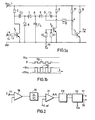
- Figure 1a is the electronic diagram of a basic cell according to the invention and Figure 1b a time diagram of certain signals used to explain its operation.
- Figure 2 is a block diagram of the signal processing chain from a sensor, incorporating a safety logic circuit for the development of signals according to the invention.
- FIG. 3a is the electronic diagram of the safety logic circuit for the preparation of the signals according to the invention
- FIG. 3b a time diagram of certain signals used to explain its operation.
- FIG. 4a is the electronic diagram of a "AND" logic gate circuit or of an inverter according to the invention.
- FIG. 4b is a time diagram of certain signals used to explain the operation of the "AND" gate circuit shown in FIG. 4a.
- FIG. 4c is a time diagram of certain signals used to explain the operation of the inverter represented in FIG. 4a.
- FIG. 5 is the electronic diagram of an attraction timer incorporating a reset circuit according to the invention.
- FIG. 6 is the electronic diagram of a positive safety memory according to the invention.
- FIG. 7 is the block diagram of an attraction timer, incorporating a reset circuit and a reset control memory according to the invention.
- FIG. 8 is the block diagram of a fall timer according to the invention.
- FIG. 1a represents a basic cell according to the invention.
- This cell comprises a first NPN transistor T 1 , the collector of which is connected to the supply terminal 1 by a resistor 2 and the emitter to ground.
- the base of T 1 receives, via a resistor 3 a useful signal Su applied to an input terminal 4, which is considered to carry the logic value "1" when it is alternating with a predetermined frequency and square (duty cycle around 0.5) and as being "0" when it is continuous.
- At least one diode pump consisting of a capacitor C 1 and two diodes 6 and 7 is used to bring the potential of a first point A to a value between 0 and -V cc .
- the capacitor C 1 and the diode 6 in the passing direction arranged in series bypass the collector-emitter path of T, and the point A is connected via the diode 7 in the direction passing to the point common to the elements C 1 and 6.
- a buffer capacitor C 3 which is part of the diode pump connects the point A to the ground.
- the basic cell further comprises a sub-assembly consisting of two xth NPN transistor T 2 , with a collector resistor 8, and a voltage shift capacitor C 2 connected between the collector of T 2 and a second point B itself connected to point A via a diode in the passing direction, 9.
- T 2 The base of T 2 is connected to ground by a bias resistor 11 and, via a resistor 12 to a terminal 13 which is the seat of an auxiliary signal Sa, likewise nature than S u , but whose frequency may be different from that of S u , in the logical state "1".
- auxiliary signal Sa likewise nature than S u , but whose frequency may be different from that of S u , in the logical state "1".
- Point A acting as a negative voltage source when T 2 is blocked, C 2 charges at the voltage 2 V DC with a positive polarity on the collector side of T 2 , point B then carrying substantially the same voltage as the point A.
- V cc When T 2 becomes saturated the potential on the two armatures of C 2 decreases suddenly by the value V cc so that the voltage in B becomes equal to a value slightly greater than -2 V DC .
- the basic cell also has an output stage consisting of a third transistor T 3 , with a collector resistor 14, and a group of two resistors 16 and 17, arranged in series between point B and terminal 1 and whose common point P (third point) is connected to the base of T 3 .
- the output signal S s of the basic cell is taken from the collector of T 3 .
- the values of resistors 16 and 17 are determined in such a way that in steady state and for S u and Sa equal to "1", the voltage of point P alternates around 0 at the rate of Sa. We have shown in FIG.
- the charge of C 2 is carried out by taking part of the energy of C 3 .
- C 3 is charged thanks to C 1 and is partially discharged by C 2 .
- S u and S a must be of the same frequency and in phase opposition. When this is the case, it is possible to omit the buffer capacitor C 3 , while obtaining the same operation as that described above, and the correct operation of the new circuit thus obtained is then a guarantee that the opposition of phase between the signals S u and S a is well respected, which may be desirable for safety reasons.
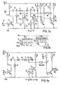
- Figure 2 shows the signal processing chain from a sensor.
- the signals used in the safety logic circuits of the invention must be alternating, rectangular in shape with a duty cycle of 0.5 and possibly of the same frequency and out of phase with each other. (case of logical "AND" in particular as described below with reference to FIG. 4a).
- the available signals generally do not meet any of the above criteria. Hence the need to develop signals that meet these criteria.
- the signals received (S) from channel sensors in particular are alternating signals (rectangular or sinusoidal). It can also be continuous signals which are then previously transformed into sinusoidal signals by means of an oscillator.
- FIG. 2 represents the cascade arrangement, between an input terminal 20, seat of a signal S, and two complementary output terminals S 8 and Ss, of an amplifier 18, a bandpass filter 19, a comparator 21, a shaping circuit 22 and a safety logic circuit for the preparation of the signals according to the invention, 23.
- the detection of a signal S which must be transformed into a useful signal takes place through the elements 18, 19 and 21.
- the frequency of S (39 kHz or 50 kHz for example) is selected through the bandpass filter 19 and its amplitude is compared at 21 with a threshold voltage V ref applied to a second input of comparator 21.
- the signal S is only transmitted to the output of 21 when its amplitude is greater than that of V ref .
- the signal from the comparator 21 is rectangular but with a duty cycle other than 0.5 generally.
- the signal is then treated at 23 as described below with reference to FIGS. 3a and 3b.
- FIG. 3a the same references designate the same elements as in FIG. 1a with the same functions but with values which may be different.
- capacitor C 3 a safety capacitor with controlled armatures C 31 is used.
- a second output stage, similar to stage T 3 , 14, 16 and 17 is used to obtain the signal S S complementary to the signal S s .
- This second stage consists of the transistor T 4 with its collector resistor 24 and the group of resistors 26 and 27 which have the point P 1 in common.
- the choice of the values of the resistors 26 and 27 is such that when S u and Sa are in the state "1" the voltage of P 1 , V P1 , remains less than 0 (left part of FIG.
- the circuit 23 is used in particular to effect a frequency change: S u being, in the state "1" for example at the frequency 39 kHz or 50 kHz and Sa at 20 kHz, an output signal at 20 is obtained for S s kHz.
- the buffer capacitor is with controlled armatures and has for this purpose four connecting conductors, the conductor 28 connected to the anode of the diode 7, the conductor 29 connected at the cathode of diode 9, the conductor 31 connected to the cathode of diode 6 and the conductor 32 connected to ground. If the buffer capacitor was similar to C 3 ( Figure 1a) and there is a break in one or the other connecting conductor, we would end up with an electronic circuit operating intermittently.
- the circuit conforming to FIG. 2 makes it possible to develop, from an analog quantity of any waveform and of selected frequency, a square alternating signal of cyclic ratio 0.5, of defined frequency (frequency of Sa the second input of circuit 23) as well as a complementary signal in the Boolean sense of the term, the system being intrinsically safe.
- FIG. 4a represents the structure of a basic cell, in which the capacitor C 3 is not used, intended to function either as an "AND” gate circuit, or as an inverter according to the values given to the group of resistors of the output stage.
- the capacitor C 3 is eliminated because the two input signals are, at state "1", of the same frequency (typically equal to 20 kHz) and phase shifted substantially by II, and it is desired that when it does not this is not so, the "AND” circuit or the inverter produces a logic output signal "0", which goes in the direction of safety, the failure thus caused making it possible to detect the nonconformity of the input signals to waveforms that must exist in normal operation.
- FIG. 4a makes it possible to explain the operation of the "AND" gate circuit by giving a representation of the voltages V B and Vp with respect to the four voltage levels: V DC , 0, -V DC and -2 V DC , as on Figures 1b and 3b.
- the input terminal 4 is the seat of a useful signal S u and the input terminal 13 receives an auxiliary signal Sa normally always in the state "1 ", the signals S u and Sa having to present, in state” 1 "the same frequency and phase characteristics as the signals S u and S ' u already described.
- the resistors belonging to the group of resistors of the output stage are of type 26 and 27 (see FIG. 3a and the description which relates to it). The inverter operation is easily deduced from the values of the voltages V B and Vp shown in FIG.
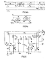
- FIG. 5 represents an attraction timer (TA) with a reset circuit.
- the upper part of the diagram represents the elementary TA whose structure is very close to that of the basic cell, the same references designating the same elements with the same functions.
- the capacitor C 3 is absent and, to ensure the phase opposition, necessary in this case between the signal on the basis of T 1 and the signal on the basis of T 2 , the base of T 2 is connected to the collector of T 1 via a resistor 28.
- the signal S u on terminal 4 constitutes the single input of the elementary TA.
- the time delay, of the order of several seconds, is provided by the capacitor C 2 , the capacity of which is several orders of magnitude higher than in the logic circuits described above.
- the capacity of C 2 is equal to 100 ⁇ F, that of C 1 being 3.9 nF.
- the elementary TA described above which creates a delay for example equal to 5 s between the appearance of S u and the appearance of S s is at the same time a fall timer (TC) because of the high capacity of C 2 .
- TC fall timer
- the circuit of FIG. 5 has at its lower part a reset circuit connected between terminal 4 and point B of the elementary TA, the function of which is to discharge very quickly the capacitor C 2 from the passage from "1" to "0" of the signal S u .
- the left part 29 of the reset circuit delimited by a rectangle in broken lines and connected to terminal 4 by a conductor 30 is a diode pump similar to that of the basic cell and intended to carry the voltage of point A 'homologous to the point A at the value -V DC in the presence of an AC signal at the input.
- the right side of the reset circuit is an output circuit with two transistors: a point P 2 is connected to point A 'via a resistor 31 and a diode 32 in the passing direction, to the power supply V cc via a resistor 33 and at the base of an NPN transistor T 6 whose emitter is connected directly to ground and the collector to the supply V cc via a resistor 34
- the collector of T 5 is also connected via a resistor 36 to the base of a PNP transistor T 6 , the emitter of which is connected to the supply V cc and the collector at point B of the elementary TA by the output conductor 37.
- the choice of the values of the resistors 31 and 33 is such that when the signal S u passes from the state "0" to the state "1", the point A 'being substantially at -V cc , the point P 2 is brought to a negative voltage, which blocks the transistor T 5 and consequently the transistor T 6 . Under these conditions, no current flows through the conductor 37, everything happens as if the reset circuit was absent and the timer operates at TA as described above, given that the capacitance values of C 4 (equivalent of C 1 ) and of C 5 (equivalent of C 3 ) are very weak and for example equal to 6.8 nF for C 4 and to 47 nF for C 5 .
- the operation in TA alone is important during successive passages of S u from state "1" to state "0" and vice versa at a rate whose period is clearly less than the time provided for the time delay at attraction.
- An example of such a sequence is the passage of a train such that during the passage of each axle of the train above the sensor, S u is brought to the state "1" while it is at "0" between two axles, the time delay at the attraction which is used being that which begins when the last axle passes.
- an elementary TA C 2 would be loaded and unloaded alternately at the rate of the passage of the axles so that the load of C 2 would gradually increase during the passage of each axle without, however, passing S s to the state "1".
- the load of C 2 would not be negligible, depending on the speed of the train and the number of axles, which would distort the time of appearance of S s with respect to said instant , by shortening this time compared to the predetermined attraction delay time. Thanks to the reset circuit, the capacitor C 2 discharges completely between the passage of two successive axles and the delay time to the predetermined attraction after the passage of the last axle is well respected. As is the case for any safety circuit used in railway signaling, any failure must be considered and it must be verified that this failure leads to a safety state higher than that which existed before the failure.
- the reset circuit can, in particular, be subject to breakdowns which, given its connection to the elementary TA can react on the latter in two ways: whatever the logical state of S u , or else the potential of point B is maintained at the voltage V cc (in the case of the interruption of the conductor 30 in particular), or else the potential of point B is no longer subjected to the action of the reset circuit (case of interruption of the conductor 37 in particular).
- the signal S s is always in the state "0", which goes in the direction of increased safety.
- the TA presents the fault indicated above, this fault however being able to allow the operation of the logic assembly (of the pedal for example) but with an uncontrollable variation of the delay time at the attraction , which may result in decreased security.
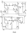
- a safety memory can be added to the circuit of FIG. 5 as described with reference to FIG. 6.
- the circuit shown in FIG. 6 is a positive memory, that is to say that it memorizes the appearance of an alternating signal on an input terminal, in this case the passage of the useful signal S u over input 4 from state "0" to state "1" whatever the subsequent logical transitions of S u .
- the memory includes the broken line conductor 38 and does not include the broken line conductor 39 which receives the voltage V cc on a terminal 40.
- part of the memory is made up of the basic cell, which is indicated by the same references.
- the auxiliary signal Sa on terminal 13 is normally always present. However, terminal 13 can constitute a validation input, the memory being validated when S a is in the state "1" and not validated when S a is in the state "0".
- the memory includes a loop-back conductor 41 which connects the collector of T 3 to an input stage constituted by a transistor T 7 and three resistors 42,43,44.
- the collector of T 7 is connected to terminal 1, its transmitter at the base of T 1 via the resistor 42 and to the ground via the resistor 43, and its base to the conductor 41 by the intermediate of resistor 44.
- Sa being in state “1” the transition "0" ⁇ "1" of S u almost immediately causes that of S s and the feedback of the output of T 3 on the basis of T 1 .
- the conductor 38 is replaced by the conductor 39 which is connected to the supply terminals of the resistors 8, 14 and 17 by means of a switch K which depends for example on the closing or on opening a user relay contact.
- switch K When switch K is closed, the memory operates as described above.
- the signal Sa When K is open, the signal Sa is in the state "0" whatever the state of the logic signal inputs S u and Sa.
- This memorization is possible provided that the time difference between the presence of the state "1" in 4 and the closing time of K is small and that the capacitance of the capacitor C 3 is determined accordingly so that its discharge time is greater than said time difference.
- FIG. 7 represents an elementary TA 46 with RESET 47 as well as their connecting conductors 30 and 37 and a RESET control memory 48 arranged upstream of the assembly 46, 47.
- the memory 48 is for example of the type comprising the conductor 38 and not including the conductor 39.
- the input signals are inverted, S u being applied to terminal 13 and Sa to terminal 4.
- a conductor 49 connects point B of the elementary TA to a known circuit with a transistor, two diodes and a resistor, not shown, placed as an additional input stage of the memory and whose function is to transmit the state "1" of the logic signal Sa at the base of the transistor T 1 of the memory when the conductor 49 is the seat of the voltage V cc and transforming this state "1" into the state "0" on the basis of T 1 when the conductor 49 is at substantially zero voltage.
- the input terminal 4 thus becomes a validation input such that the transition to the state "1" of the signal S u can only be transmitted, through the memory 48, at the input of the TA 46 and of its RESET 47 only if , during the state "0" of S u preceding its passage to the state "1", the voltage V cc is applied by the RESET 47 at point B of the elementary TA 46.
- the electronic assembly conforms to the diagram of FIG. 7 therefore constitutes a TA not operating in TC and such that any failure results in the passage and maintenance of the state "0" of the signal S s , whatever the logical state of the signal S u .
- the block diagram of FIG. 8 represents a fall timer (TC) comprising a first basic cell 51, a second basic cell 52, a memory 53 and an "OR" gate circuit 54.
- Cell 51 receives the signal S u on its terminal 4 and the signal Sa on its terminal 13 (not shown).
- the cell 52 receives on its input 4 (not shown) the output signal from the cell 51, and the signal Sa on its terminal 13 (not shown).
- the memory 53 receives on its terminal 4 (not shown) the signal S u and on its terminal 13 (not shown) the output signal from the "OR” gate circuit 54, the two inputs of which are connected to the respective outputs of the cells 51 and 52.
- the capacitors of the capacitors C l , C 2 and C 3 of the memory 53 are low so that the response time of the memory is low.
- the CT of FIG. 8 has a TA time at least equal to the cumulative TA times of cell 51 and of memory 53.
- the invention is not limited to railway signaling. It generally applies to any automation requiring very high operational safety.
Landscapes
- Physics & Mathematics (AREA)
- Engineering & Computer Science (AREA)
- Computer Hardware Design (AREA)
- Computing Systems (AREA)
- General Engineering & Computer Science (AREA)
- Mathematical Physics (AREA)
- Electronic Switches (AREA)
- Logic Circuits (AREA)
Applications Claiming Priority (2)
| Application Number | Priority Date | Filing Date | Title |
|---|---|---|---|
| FR8114945A FR2510845A1 (fr) | 1981-07-31 | 1981-07-31 | Circuits logiques de securite utilisables notamment en signalisation ferroviaire et boite de traitement electronique, ou automatisme incorporant au moins un de ces circuits |
| FR8114945 | 1981-07-31 |
Publications (2)
| Publication Number | Publication Date |
|---|---|
| EP0074674A1 EP0074674A1 (fr) | 1983-03-23 |
| EP0074674B1 true EP0074674B1 (fr) | 1988-06-01 |
Family
ID=9261057
Family Applications (1)
| Application Number | Title | Priority Date | Filing Date |
|---|---|---|---|
| EP19820200934 Expired EP0074674B1 (fr) | 1981-07-31 | 1982-07-22 | Circuits logiques de sécurité utilisables notamment en signalisation ferroviaire |
Country Status (3)
| Country | Link |
|---|---|
| EP (1) | EP0074674B1 (Direct) |
| DE (1) | DE3278612D1 (Direct) |
| FR (1) | FR2510845A1 (Direct) |
Families Citing this family (5)
| Publication number | Priority date | Publication date | Assignee | Title |
|---|---|---|---|---|
| FR2553605B1 (fr) * | 1983-10-13 | 1988-12-02 | Jeumont Schneider | Circuit logique a seuil et a securite intrinseque |
| DE3570963D1 (en) * | 1984-03-21 | 1989-07-13 | Siemens Ag | Circuit for memorizing dynamic logic signals |
| WO2001050604A1 (en) * | 1999-12-30 | 2001-07-12 | Ge-Harris Railway Electronics, Llc | Vital 'and' gate apparatus and method |
| FR2808631B1 (fr) * | 2000-05-03 | 2002-07-19 | Erim S A | Dispositif d'entree logique pour automate |
| FR2870652B1 (fr) * | 2004-05-24 | 2007-08-03 | Scle Soc De Construction De Li | Dispositif de securite reproduisant une fonction logique notamment un "et" de securite |
Family Cites Families (3)
| Publication number | Priority date | Publication date | Assignee | Title |
|---|---|---|---|---|
| NL274016A (Direct) * | 1961-01-26 | |||
| FR1391823A (fr) * | 1964-01-08 | 1965-03-12 | Westinghouse Freins & Signaux | Circuit logique de sécurité du type et |
| FR1398923A (fr) * | 1964-04-03 | 1965-05-14 | Westinghouse Freins & Signaux | Mémoire électronique de sécurité |
-
1981
- 1981-07-31 FR FR8114945A patent/FR2510845A1/fr active Granted
-
1982
- 1982-07-22 EP EP19820200934 patent/EP0074674B1/fr not_active Expired
- 1982-07-22 DE DE8282200934T patent/DE3278612D1/de not_active Expired
Also Published As
| Publication number | Publication date |
|---|---|
| DE3278612D1 (en) | 1988-07-07 |
| FR2510845A1 (fr) | 1983-02-04 |
| FR2510845B1 (Direct) | 1983-11-10 |
| EP0074674A1 (fr) | 1983-03-23 |
Similar Documents
| Publication | Publication Date | Title |
|---|---|---|
| FR2533183A1 (fr) | Methode et arrangement de circuits pour commander un appareillage de commande de glissement de freinage | |
| EP0171635B1 (fr) | Procédé et dispositif de reconnaissance de la position du rotor d'un moteur pas à pas | |
| FR2623652A1 (fr) | Unite de memoire statique a plusieurs modes de test et ordinateur muni de telles unites | |
| FR3017958A1 (fr) | Detection de circuit ouvert dans une structure de commutation | |
| EP0364314A1 (fr) | Procédé de lecture de cellules photosensibles du type comportant deux diodes montées en série avec des sens de conduction opposés | |
| EP0074674B1 (fr) | Circuits logiques de sécurité utilisables notamment en signalisation ferroviaire | |
| CA1296059C (fr) | Dispositif pour detecter les coupures et les court-circuits dansau moins une portion de circuit electrique | |
| FR2753318A1 (fr) | Dispositif de mesure de courants dans un onduleur | |
| CH635280A5 (fr) | Dispositif de commande de freins a action anti-blocage d'un vehicule. | |
| EP0234968A1 (fr) | Procédé de lecture d'élément photosensible constitué d'une photodiode et d'une capacité | |
| CA3056877A1 (fr) | Architecture de systeme de freinage pour aeronef | |
| EP0201136A1 (fr) | Module multiplexeur numérique à N entrées et multiplexeur à N2 entrées incorporant de tels modules | |
| FR2757712A1 (fr) | Dispositif de controle de mise sous tension ou hors tension d'un circuit integre | |
| EP0162755B1 (fr) | Circuit de commande d'un solenoide bistable | |
| WO2011138529A1 (fr) | Procede et dispositif de caracterisation ou de mesure d'une capacite | |
| EP0029631B1 (fr) | Mémoire électronique de sécurité utilisable en signalisation ferroviaire | |
| EP0115994A1 (fr) | Interface pour relier un système informatique à un dispositif actionneur | |
| FR2879375A1 (fr) | Dispositif de reinitialisation d'un circuit integre a partir d'une detection d'une chute d'une tension d'alimentation, et circuit electronique correspondant | |
| EP0110481A1 (fr) | Système d'identification de stations locales par un poste central d'interrogation | |
| CH620533A5 (Direct) | ||
| EP0618518A1 (fr) | Interface analogique de sécurité | |
| EP0961207B1 (fr) | Dispositif de communication entre un réseau neuronal et un système utilisateur par l'intermédiaire d'un bus | |
| EP0324524B1 (fr) | Détecteur de positionnement | |
| FR2719126A1 (fr) | Circuit de mesure pour ensemble modulaire de cellules électriques raccordées en série, notamment pour ensemble de type batterie d'accumulateur. | |
| EP3779611B1 (fr) | Montre électromécanique |
Legal Events
| Date | Code | Title | Description |
|---|---|---|---|
| PUAI | Public reference made under article 153(3) epc to a published international application that has entered the european phase |
Free format text: ORIGINAL CODE: 0009012 |
|
| 17P | Request for examination filed |
Effective date: 19820722 |
|
| AK | Designated contracting states |
Designated state(s): BE CH DE FR GB IT LI NL SE |
|
| REG | Reference to a national code |
Ref country code: FR Ref legal event code: CL |
|
| GRAA | (expected) grant |
Free format text: ORIGINAL CODE: 0009210 |
|
| AK | Designated contracting states |
Kind code of ref document: B1 Designated state(s): BE CH DE FR GB IT LI NL SE |
|
| PG25 | Lapsed in a contracting state [announced via postgrant information from national office to epo] |
Ref country code: NL Effective date: 19880601 Ref country code: IT Free format text: LAPSE BECAUSE OF FAILURE TO SUBMIT A TRANSLATION OF THE DESCRIPTION OR TO PAY THE FEE WITHIN THE PRESCRIBED TIME-LIMIT;WARNING: LAPSES OF ITALIAN PATENTS WITH EFFECTIVE DATE BEFORE 2007 MAY HAVE OCCURRED AT ANY TIME BEFORE 2007. THE CORRECT EFFECTIVE DATE MAY BE DIFFERENT FROM THE ONE RECORDED. Effective date: 19880601 |
|
| REF | Corresponds to: |
Ref document number: 3278612 Country of ref document: DE Date of ref document: 19880707 |
|
| PG25 | Lapsed in a contracting state [announced via postgrant information from national office to epo] |
Ref country code: SE Effective date: 19880723 |
|
| PG25 | Lapsed in a contracting state [announced via postgrant information from national office to epo] |
Ref country code: LI Effective date: 19880731 Ref country code: CH Effective date: 19880731 Ref country code: BE Effective date: 19880731 |
|
| NLV1 | Nl: lapsed or annulled due to failure to fulfill the requirements of art. 29p and 29m of the patents act | ||
| PG25 | Lapsed in a contracting state [announced via postgrant information from national office to epo] |
Ref country code: GB Free format text: LAPSE BECAUSE OF NON-PAYMENT OF DUE FEES Effective date: 19881121 |
|
| GBV | Gb: ep patent (uk) treated as always having been void in accordance with gb section 77(7)/1977 [no translation filed] | ||
| BERE | Be: lapsed |
Owner name: PHILIPS' GLOEILAMPENFABRIEKEN N.V. Effective date: 19880731 |
|
| PLBE | No opposition filed within time limit |
Free format text: ORIGINAL CODE: 0009261 |
|
| REG | Reference to a national code |
Ref country code: CH Ref legal event code: PL |
|
| STAA | Information on the status of an ep patent application or granted ep patent |
Free format text: STATUS: NO OPPOSITION FILED WITHIN TIME LIMIT |
|
| PG25 | Lapsed in a contracting state [announced via postgrant information from national office to epo] |
Ref country code: DE Effective date: 19890401 |
|
| 26N | No opposition filed | ||
| PG25 | Lapsed in a contracting state [announced via postgrant information from national office to epo] |
Ref country code: FR Free format text: LAPSE BECAUSE OF NON-PAYMENT OF DUE FEES Effective date: 19900330 |
|
| REG | Reference to a national code |
Ref country code: FR Ref legal event code: TP |
|
| REG | Reference to a national code |
Ref country code: FR Ref legal event code: ST |
|
| EUG | Se: european patent has lapsed |
Ref document number: 82200934.6 Effective date: 19890510 |