EP0073075A2 - Dispositif semi-conducteur comprenant du silicium polycristallin et procédé pour la fabrication du dispositif - Google Patents
Dispositif semi-conducteur comprenant du silicium polycristallin et procédé pour la fabrication du dispositif Download PDFInfo
- Publication number
- EP0073075A2 EP0073075A2 EP82200965A EP82200965A EP0073075A2 EP 0073075 A2 EP0073075 A2 EP 0073075A2 EP 82200965 A EP82200965 A EP 82200965A EP 82200965 A EP82200965 A EP 82200965A EP 0073075 A2 EP0073075 A2 EP 0073075A2
- Authority
- EP
- European Patent Office
- Prior art keywords
- polycrystalline silicon
- semiconductor device
- carbon
- doped
- silicon
- Prior art date
- Legal status (The legal status is an assumption and is not a legal conclusion. Google has not performed a legal analysis and makes no representation as to the accuracy of the status listed.)
- Granted
Links
- 229910021420 polycrystalline silicon Inorganic materials 0.000 title claims abstract description 51
- 239000004065 semiconductor Substances 0.000 title claims abstract description 38
- 238000000034 method Methods 0.000 title description 5
- 229910052799 carbon Inorganic materials 0.000 claims abstract description 29
- OKTJSMMVPCPJKN-UHFFFAOYSA-N Carbon Chemical compound [C] OKTJSMMVPCPJKN-UHFFFAOYSA-N 0.000 claims abstract description 28
- XUIMIQQOPSSXEZ-UHFFFAOYSA-N Silicon Chemical group [Si] XUIMIQQOPSSXEZ-UHFFFAOYSA-N 0.000 claims description 12
- 238000009792 diffusion process Methods 0.000 claims description 11
- 238000004519 manufacturing process Methods 0.000 claims description 11
- 239000002019 doping agent Substances 0.000 claims description 10
- HSFWRNGVRCDJHI-UHFFFAOYSA-N Acetylene Chemical compound C#C HSFWRNGVRCDJHI-UHFFFAOYSA-N 0.000 claims description 8
- 150000001722 carbon compounds Chemical class 0.000 claims description 5
- 150000003377 silicon compounds Chemical class 0.000 claims description 3
- 238000011282 treatment Methods 0.000 abstract description 10
- 229920005591 polysilicon Polymers 0.000 abstract description 4
- 229910052710 silicon Inorganic materials 0.000 description 10
- 239000010703 silicon Substances 0.000 description 10
- 239000013078 crystal Substances 0.000 description 8
- 239000000463 material Substances 0.000 description 7
- VYPSYNLAJGMNEJ-UHFFFAOYSA-N Silicium dioxide Chemical compound O=[Si]=O VYPSYNLAJGMNEJ-UHFFFAOYSA-N 0.000 description 5
- OAICVXFJPJFONN-UHFFFAOYSA-N Phosphorus Chemical compound [P] OAICVXFJPJFONN-UHFFFAOYSA-N 0.000 description 4
- 229910052698 phosphorus Inorganic materials 0.000 description 4
- 239000011574 phosphorus Substances 0.000 description 4
- 230000004913 activation Effects 0.000 description 3
- 238000007669 thermal treatment Methods 0.000 description 3
- 229910021417 amorphous silicon Inorganic materials 0.000 description 2
- 230000015572 biosynthetic process Effects 0.000 description 2
- 239000004020 conductor Substances 0.000 description 2
- 238000009826 distribution Methods 0.000 description 2
- 238000005530 etching Methods 0.000 description 2
- 238000010348 incorporation Methods 0.000 description 2
- 238000009413 insulation Methods 0.000 description 2
- 229910021421 monocrystalline silicon Inorganic materials 0.000 description 2
- XHXFXVLFKHQFAL-UHFFFAOYSA-N phosphoryl trichloride Chemical compound ClP(Cl)(Cl)=O XHXFXVLFKHQFAL-UHFFFAOYSA-N 0.000 description 2
- 235000012239 silicon dioxide Nutrition 0.000 description 2
- 239000000377 silicon dioxide Substances 0.000 description 2
- UFHFLCQGNIYNRP-UHFFFAOYSA-N Hydrogen Chemical compound [H][H] UFHFLCQGNIYNRP-UHFFFAOYSA-N 0.000 description 1
- 229910019213 POCl3 Inorganic materials 0.000 description 1
- 238000002441 X-ray diffraction Methods 0.000 description 1
- 125000004429 atom Chemical group 0.000 description 1
- QVGXLLKOCUKJST-UHFFFAOYSA-N atomic oxygen Chemical compound [O] QVGXLLKOCUKJST-UHFFFAOYSA-N 0.000 description 1
- 125000004432 carbon atom Chemical group C* 0.000 description 1
- 239000012159 carrier gas Substances 0.000 description 1
- 239000002800 charge carrier Substances 0.000 description 1
- 230000001419 dependent effect Effects 0.000 description 1
- 229910052739 hydrogen Inorganic materials 0.000 description 1
- 239000001257 hydrogen Substances 0.000 description 1
- 238000002513 implantation Methods 0.000 description 1
- 238000005468 ion implantation Methods 0.000 description 1
- 230000000873 masking effect Effects 0.000 description 1
- 238000001465 metallisation Methods 0.000 description 1
- 229910052760 oxygen Inorganic materials 0.000 description 1
- 239000001301 oxygen Substances 0.000 description 1
- 238000002161 passivation Methods 0.000 description 1
- HBMJWWWQQXIZIP-UHFFFAOYSA-N silicon carbide Chemical compound [Si+]#[C-] HBMJWWWQQXIZIP-UHFFFAOYSA-N 0.000 description 1
- 229910010271 silicon carbide Inorganic materials 0.000 description 1
- 229910052814 silicon oxide Inorganic materials 0.000 description 1
- 239000000126 substance Substances 0.000 description 1
- 239000000758 substrate Substances 0.000 description 1
- 238000005496 tempering Methods 0.000 description 1
Images
Classifications
-
- H—ELECTRICITY
- H01—ELECTRIC ELEMENTS
- H01L—SEMICONDUCTOR DEVICES NOT COVERED BY CLASS H10
- H01L21/00—Processes or apparatus adapted for the manufacture or treatment of semiconductor or solid state devices or of parts thereof
- H01L21/02—Manufacture or treatment of semiconductor devices or of parts thereof
- H01L21/04—Manufacture or treatment of semiconductor devices or of parts thereof the devices having at least one potential-jump barrier or surface barrier, e.g. PN junction, depletion layer or carrier concentration layer
- H01L21/18—Manufacture or treatment of semiconductor devices or of parts thereof the devices having at least one potential-jump barrier or surface barrier, e.g. PN junction, depletion layer or carrier concentration layer the devices having semiconductor bodies comprising elements of Group IV of the Periodic System or AIIIBV compounds with or without impurities, e.g. doping materials
- H01L21/28—Manufacture of electrodes on semiconductor bodies using processes or apparatus not provided for in groups H01L21/20 - H01L21/268
- H01L21/28008—Making conductor-insulator-semiconductor electrodes
- H01L21/28017—Making conductor-insulator-semiconductor electrodes the insulator being formed after the semiconductor body, the semiconductor being silicon
- H01L21/28026—Making conductor-insulator-semiconductor electrodes the insulator being formed after the semiconductor body, the semiconductor being silicon characterised by the conductor
- H01L21/28035—Making conductor-insulator-semiconductor electrodes the insulator being formed after the semiconductor body, the semiconductor being silicon characterised by the conductor the final conductor layer next to the insulator being silicon, e.g. polysilicon, with or without impurities
-
- H—ELECTRICITY
- H01—ELECTRIC ELEMENTS
- H01L—SEMICONDUCTOR DEVICES NOT COVERED BY CLASS H10
- H01L21/00—Processes or apparatus adapted for the manufacture or treatment of semiconductor or solid state devices or of parts thereof
- H01L21/02—Manufacture or treatment of semiconductor devices or of parts thereof
- H01L21/02104—Forming layers
- H01L21/02365—Forming inorganic semiconducting materials on a substrate
- H01L21/02518—Deposited layers
- H01L21/02521—Materials
- H01L21/02524—Group 14 semiconducting materials
- H01L21/02529—Silicon carbide
-
- H—ELECTRICITY
- H01—ELECTRIC ELEMENTS
- H01L—SEMICONDUCTOR DEVICES NOT COVERED BY CLASS H10
- H01L21/00—Processes or apparatus adapted for the manufacture or treatment of semiconductor or solid state devices or of parts thereof
- H01L21/02—Manufacture or treatment of semiconductor devices or of parts thereof
- H01L21/02104—Forming layers
- H01L21/02365—Forming inorganic semiconducting materials on a substrate
- H01L21/02518—Deposited layers
- H01L21/02521—Materials
- H01L21/02524—Group 14 semiconducting materials
- H01L21/02532—Silicon, silicon germanium, germanium
-
- H—ELECTRICITY
- H01—ELECTRIC ELEMENTS
- H01L—SEMICONDUCTOR DEVICES NOT COVERED BY CLASS H10
- H01L21/00—Processes or apparatus adapted for the manufacture or treatment of semiconductor or solid state devices or of parts thereof
- H01L21/02—Manufacture or treatment of semiconductor devices or of parts thereof
- H01L21/02104—Forming layers
- H01L21/02365—Forming inorganic semiconducting materials on a substrate
- H01L21/02518—Deposited layers
- H01L21/0257—Doping during depositing
- H01L21/02573—Conductivity type
- H01L21/02576—N-type
-
- H—ELECTRICITY
- H01—ELECTRIC ELEMENTS
- H01L—SEMICONDUCTOR DEVICES NOT COVERED BY CLASS H10
- H01L21/00—Processes or apparatus adapted for the manufacture or treatment of semiconductor or solid state devices or of parts thereof
- H01L21/02—Manufacture or treatment of semiconductor devices or of parts thereof
- H01L21/02104—Forming layers
- H01L21/02365—Forming inorganic semiconducting materials on a substrate
- H01L21/02518—Deposited layers
- H01L21/0257—Doping during depositing
- H01L21/02573—Conductivity type
- H01L21/02579—P-type
-
- H—ELECTRICITY
- H01—ELECTRIC ELEMENTS
- H01L—SEMICONDUCTOR DEVICES NOT COVERED BY CLASS H10
- H01L21/00—Processes or apparatus adapted for the manufacture or treatment of semiconductor or solid state devices or of parts thereof
- H01L21/02—Manufacture or treatment of semiconductor devices or of parts thereof
- H01L21/04—Manufacture or treatment of semiconductor devices or of parts thereof the devices having at least one potential-jump barrier or surface barrier, e.g. PN junction, depletion layer or carrier concentration layer
- H01L21/18—Manufacture or treatment of semiconductor devices or of parts thereof the devices having at least one potential-jump barrier or surface barrier, e.g. PN junction, depletion layer or carrier concentration layer the devices having semiconductor bodies comprising elements of Group IV of the Periodic System or AIIIBV compounds with or without impurities, e.g. doping materials
- H01L21/28—Manufacture of electrodes on semiconductor bodies using processes or apparatus not provided for in groups H01L21/20 - H01L21/268
- H01L21/28008—Making conductor-insulator-semiconductor electrodes
- H01L21/28017—Making conductor-insulator-semiconductor electrodes the insulator being formed after the semiconductor body, the semiconductor being silicon
- H01L21/28026—Making conductor-insulator-semiconductor electrodes the insulator being formed after the semiconductor body, the semiconductor being silicon characterised by the conductor
- H01L21/2807—Making conductor-insulator-semiconductor electrodes the insulator being formed after the semiconductor body, the semiconductor being silicon characterised by the conductor the final conductor layer next to the insulator being Si or Ge or C and their alloys except Si
-
- H—ELECTRICITY
- H01—ELECTRIC ELEMENTS
- H01L—SEMICONDUCTOR DEVICES NOT COVERED BY CLASS H10
- H01L21/00—Processes or apparatus adapted for the manufacture or treatment of semiconductor or solid state devices or of parts thereof
- H01L21/02—Manufacture or treatment of semiconductor devices or of parts thereof
- H01L21/04—Manufacture or treatment of semiconductor devices or of parts thereof the devices having at least one potential-jump barrier or surface barrier, e.g. PN junction, depletion layer or carrier concentration layer
- H01L21/18—Manufacture or treatment of semiconductor devices or of parts thereof the devices having at least one potential-jump barrier or surface barrier, e.g. PN junction, depletion layer or carrier concentration layer the devices having semiconductor bodies comprising elements of Group IV of the Periodic System or AIIIBV compounds with or without impurities, e.g. doping materials
- H01L21/30—Treatment of semiconductor bodies using processes or apparatus not provided for in groups H01L21/20 - H01L21/26
- H01L21/31—Treatment of semiconductor bodies using processes or apparatus not provided for in groups H01L21/20 - H01L21/26 to form insulating layers thereon, e.g. for masking or by using photolithographic techniques; After treatment of these layers; Selection of materials for these layers
- H01L21/3205—Deposition of non-insulating-, e.g. conductive- or resistive-, layers on insulating layers; After-treatment of these layers
- H01L21/32055—Deposition of semiconductive layers, e.g. poly - or amorphous silicon layers
-
- H—ELECTRICITY
- H01—ELECTRIC ELEMENTS
- H01L—SEMICONDUCTOR DEVICES NOT COVERED BY CLASS H10
- H01L29/00—Semiconductor devices adapted for rectifying, amplifying, oscillating or switching, or capacitors or resistors with at least one potential-jump barrier or surface barrier, e.g. PN junction depletion layer or carrier concentration layer; Details of semiconductor bodies or of electrodes thereof ; Multistep manufacturing processes therefor
- H01L29/02—Semiconductor bodies ; Multistep manufacturing processes therefor
- H01L29/04—Semiconductor bodies ; Multistep manufacturing processes therefor characterised by their crystalline structure, e.g. polycrystalline, cubic or particular orientation of crystalline planes
-
- H—ELECTRICITY
- H01—ELECTRIC ELEMENTS
- H01L—SEMICONDUCTOR DEVICES NOT COVERED BY CLASS H10
- H01L29/00—Semiconductor devices adapted for rectifying, amplifying, oscillating or switching, or capacitors or resistors with at least one potential-jump barrier or surface barrier, e.g. PN junction depletion layer or carrier concentration layer; Details of semiconductor bodies or of electrodes thereof ; Multistep manufacturing processes therefor
- H01L29/02—Semiconductor bodies ; Multistep manufacturing processes therefor
- H01L29/12—Semiconductor bodies ; Multistep manufacturing processes therefor characterised by the materials of which they are formed
- H01L29/16—Semiconductor bodies ; Multistep manufacturing processes therefor characterised by the materials of which they are formed including, apart from doping materials or other impurities, only elements of Group IV of the Periodic System
- H01L29/167—Semiconductor bodies ; Multistep manufacturing processes therefor characterised by the materials of which they are formed including, apart from doping materials or other impurities, only elements of Group IV of the Periodic System further characterised by the doping material
-
- Y—GENERAL TAGGING OF NEW TECHNOLOGICAL DEVELOPMENTS; GENERAL TAGGING OF CROSS-SECTIONAL TECHNOLOGIES SPANNING OVER SEVERAL SECTIONS OF THE IPC; TECHNICAL SUBJECTS COVERED BY FORMER USPC CROSS-REFERENCE ART COLLECTIONS [XRACs] AND DIGESTS
- Y10—TECHNICAL SUBJECTS COVERED BY FORMER USPC
- Y10S—TECHNICAL SUBJECTS COVERED BY FORMER USPC CROSS-REFERENCE ART COLLECTIONS [XRACs] AND DIGESTS
- Y10S438/00—Semiconductor device manufacturing: process
- Y10S438/914—Doping
- Y10S438/918—Special or nonstandard dopant
Definitions
- the invention relates to a semiconductor device having a semiconductor body which comprises a circuit element with a part formed from doped polycrystalline silicon.
- semiconductor device includes, for example, diodes, transistors and integrated circuits.
- Polycrystalline silicon is silicon in which crystallites can be demonstrated by X-ray analysis.
- the size of said crystallites is at least approximately 15
- grain limits in polycrystalline silicon means that, electrically, this material is inhomogeneous, while amorphous and monocrystalline silicon - in the absence of grain limits - are homogeneous materials, electrically.
- polycrystalline silicon is used for many purposes, for example, as a diffusion source on a semiconductor body, as a conductive material, for example, for gate electrodes in MOS transistors, and as a resistive material.
- the polycrystalline silicon may comprise a dopant influencing the electric conductivity, which dopant as such determines the electric conductivity in the polycrystalline silicon and/or can be transferred to a semiconductor body.
- a problem with polycrystalline silicon is that treatments at elevated temperatures, as are usual upon tempering and diffusion, for example, may give rise to reduced stability and poorer reproducibility of the semiconductor device.
- crystal growth easily occurs in 1 polycrystalline silicon when the temperature rises.
- crystal size becomes of the order of magnitude of the thickness of a polycrystalline layer, a substrate on which the layer is present can be undesirably attacked upon etching.
- One of the objects of the invention is to avoid the above problems at least to a considerable extent.
- the invention is inter alia based on the recognition of the fact that the properties of polycrystalline silicon can be improved by the-incorporation of certain substances.
- the semiconductor device mentioned in the opening paragraph is characterized in that the polycrystalline silicon is doped with carbon in a concentration which is higher than 1 part per million (ppm.).
- the conductivity of the polycrystalline silicon doped with carbon can further be adjusted particularly suitably if the polycrystalline silicon is further doped with a dopant determining the conductivity type.
- both the electric resistance and the activation azergy of the electric resistance of the polycrystalline silicon decrease when the carbon concentration increases.
- the carbon atoms are probably present at the boundaries of the silicon crystallites and increase the mobility of the charge carriers over the grain limits.
- the influence of small carbon concentrations on the resistance is small.
- both the resistance and the activation energy of the resistance increase at all phosphorus concentrations. This is associated with the presence of silicon carbide and/or carbon as the second phase beside the polycrystalline silicon. In forming polycrystalline silicon with such a carbon content and such properties the grains are generally smaller than at lower carbon content.
- the resistance and the activation energy of the resistance decrease again.
- the comparatively low resistance is possibly associated with conductivity via carbon bridges.
- the silicon in particular when low formation temperatures are used, has then become substantially amorphous.
- the polycrystalline silicon in the semiconductor device according to the invention may form the gate electrode of a MOS transistor or the polycrystalline silicon locally forms a resistor on the semiconductor body.
- the polycrystalline silicon may form a resistance layer for the draining of charge on a p-n junction, for example, in a high-voltage transistor.
- the invention furthermore relates to a method of manufacturing a semiconductor device according to the inven-0 tion.
- carbon may be implanted in a provided polycrystalline silicon layer.
- the voltage upon implantation must continually 85 be varied in the course of the process so as to adjust the desired carbon concentration in any place in the silicon.
- a temperature treatment cannot improve the homogeneity of the carbon distribution, since carbon diffuses very slowly into silicon even at elevated temperatures.
- the doped polycrystalline silicon is preferably formed from a gaseous silicon compound and a gaseous unsaturated carbon compound at a temperature above 700°C.
- Ethyne is very suitable for incorporation of carbon in the polycrystalline silicon.
- the polycrystalline silicon may be used as a diffusion source to obtain a doped region in the semiconductor body.
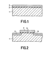
- Figures 1 and 2 of the drawing are diagrammatic sectional views of a part of a semiconductor device in successive stages of the manufacture by means of the method according to the invention.
- a semiconductor body 1 of silicon is provided at a stage of the manufacture in a usual manner with a 0.2 / um thick layer 2 of silicon dioxide on which a 0.5 / um thick layer 3 of polycrystalline silicon is provided.
- the layer 3 is doped with carbon in a concentration above 1 ppm and it is formed from a gaseous silicon compound and a gaseous unsaturated carbon compound at a temperature above 700°C.
- a carbon compound for example, ethyne (C 2 H 2 ).
- ethyne C 2 H 2
- a carbon content in layer 3 is obtained of 1000 ppm ( 5 x 10 19 at/ cm ) with a grain size of the silicon in layer 3 of 0.1 / um.
- This grain size is substantially not varied in later process steps when source and drain regions 4 and 5 of the MOS transistor are obtained.
- the polycrystalline silicon layer 3 may furthermore be doped with a dopant determining the conductivity type.
- the dopant may be present as gaseous PH 3 during the formation of layer 3.
- Said dopant may also be introduced in the already formed polycrystalline silicon by diffusion by means of a POCl 3 source or by ion implantation.
- such a thermal treatment of the polycrystalline layer is carried out in an oxygen atmosphere, in which a silicon oxide layer is formed on the polycrystalline layer.
- the gate electrode 7 is also used as a mask during the introduction of a dopant in the silicon body 1 so as to obtain the source and drain regions 4 and 5.
- An oxide layer formed during said treatments may be removed from the gate electrode by etching.
- the gate electrode has become coarse crystalline, the gate insulation below the gate electrode can also be attacked easily and short-circuit with the silicon body occurs during subsequent metallization of the gate electrode.
- a polycrystalline silicon layer is formed the crystal size of which can be chosen to be sufficiently small. Said grain size remains constant and does not increase in subsequent thermal treatments.
- Carbon-doped polycrystalline silicon layers may also be used as a resistor. They have the advantage over resistors in a monocrystalline semiconductor body that the area required for that purpose may then be used for other circuit elements.
- a polycrystalline resistor is then provided on an insulating layer and, for example via apertures in said layer, contacts an underlying monocrystalline semiconductor body and/or, via apertures in an insulating layer present on the resistor, contacts a wiring pattern present above the resistor.
- resistivities of the polycrystalline silicon between 1 and 10 5 ⁇ cm may be adjusted.
- the desired resistance can be chosen within wide limits.
- Carbon-doped polycrystalline silicon layers may also be used as a passivating layer on a p-n junction.
- a layer of high-ohmic material which also forms a controlled leakage path is often desirable.
- a 0.2 / um thick layer having a crystal size of 0.1 / um which has a resistivity of 10 10 ⁇ / ⁇ and comprises a silicon dioxide layer forms a suitable passivation for p-n junctions operated at high reverse voltage.
- Carbon-doped polycrystalline silicon layers may be used as a diffusion source so as to obtain a doped region in a semiconductor body.
- polycrystalline silicon layers as described above in connection with the manufacture of gate electrodes and resistors, are often provided as conductor tracks on and as a diffusion source in apertures of a masking layer. After the diffusion treatment the diffusion source is maintained as a contact in the apertures on the semiconductor body.
- the crystal size of the diffusion source is chosen to be small and remains constant during the diffusion treatment so that upon removing the oxide layer from the polysilicon an oxide layer, if any, present below the polysilicon is not attacked.
- Suitable temperatures for providing the polycrystalline layer are normally between 700 and 1000 0 C and the pressures used are generally between 65 and 10 D Pa.
- a semiconductor body on which the polysilicon is provided may also consist, for example, of A III B V material.
Applications Claiming Priority (2)
| Application Number | Priority Date | Filing Date | Title |
|---|---|---|---|
| NL8103649 | 1981-08-03 | ||
| NL8103649A NL8103649A (nl) | 1981-08-03 | 1981-08-03 | Halfgeleiderinrichting en werkwijze voor het vervaardigen van de halfgeleiderinrichting. |
Publications (3)
| Publication Number | Publication Date |
|---|---|
| EP0073075A2 true EP0073075A2 (fr) | 1983-03-02 |
| EP0073075A3 EP0073075A3 (en) | 1984-08-22 |
| EP0073075B1 EP0073075B1 (fr) | 1987-10-14 |
Family
ID=19837888
Family Applications (1)
| Application Number | Title | Priority Date | Filing Date |
|---|---|---|---|
| EP82200965A Expired EP0073075B1 (fr) | 1981-08-03 | 1982-07-28 | Dispositif semi-conducteur comprenant du silicium polycristallin et procédé pour la fabrication du dispositif |
Country Status (7)
| Country | Link |
|---|---|
| US (1) | US4891332A (fr) |
| EP (1) | EP0073075B1 (fr) |
| JP (1) | JPS5832471A (fr) |
| AU (1) | AU552505B2 (fr) |
| CA (1) | CA1217116A (fr) |
| DE (1) | DE3277483D1 (fr) |
| NL (1) | NL8103649A (fr) |
Cited By (3)
| Publication number | Priority date | Publication date | Assignee | Title |
|---|---|---|---|---|
| EP0222215A2 (fr) * | 1985-10-23 | 1987-05-20 | Hitachi, Ltd. | Transistor MOS en polysilicium et son procédé de fabrication |
| EP0646969A2 (fr) * | 1993-10-05 | 1995-04-05 | Motorola, Inc. | Dispositif semi-conducteur en carbone-silicium ayant un intervalle de bande rétréci et méthode pour sa fabrication |
| DE19652417A1 (de) * | 1996-12-09 | 1998-06-10 | Inst Halbleiterphysik Gmbh | MOSFET und Verfahren zur Herstellung der Schichten für einen derartigen Transistor |
Families Citing this family (9)
| Publication number | Priority date | Publication date | Assignee | Title |
|---|---|---|---|---|
| US5037766A (en) * | 1988-12-06 | 1991-08-06 | Industrial Technology Research Institute | Method of fabricating a thin film polysilicon thin film transistor or resistor |
| GB8908509D0 (en) * | 1989-04-14 | 1989-06-01 | Secr Defence | Substitutional carbon in silicon |
| US5885861A (en) * | 1997-05-30 | 1999-03-23 | Advanced Micro Devices, Inc. | Reduction of dopant diffusion by the co-implantation of impurities into the transistor gate conductor |
| US6258067B1 (en) * | 1998-12-08 | 2001-07-10 | Smith & Nephew, Inc. | Middle ear fluid aspirator |
| US6576535B2 (en) | 2001-04-11 | 2003-06-10 | Texas Instruments Incorporated | Carbon doped epitaxial layer for high speed CB-CMOS |
| US6774019B2 (en) * | 2002-05-17 | 2004-08-10 | International Business Machines Corporation | Incorporation of an impurity into a thin film |
| CA2419216C (fr) | 2003-02-19 | 2005-03-01 | Jan Nyquist | Methode et appareil de raccordement de tuyaux en plastique |
| US7736968B2 (en) * | 2008-10-27 | 2010-06-15 | Taiwan Semiconductor Manufacturing Company, Ltd. | Reducing poly-depletion through co-implanting carbon and nitrogen |
| US20120043600A1 (en) * | 2010-08-18 | 2012-02-23 | Van Der Vegt Henderikus Albert | Floating-Gate Device and Method Therefor |
Citations (4)
| Publication number | Priority date | Publication date | Assignee | Title |
|---|---|---|---|---|
| DE1521465A1 (de) * | 1964-08-04 | 1969-07-31 | Siemens Ag | Texturloses polykristallines Silicium und Verfahren zu dessen Herstellung |
| FR2011292A1 (fr) * | 1968-06-20 | 1970-02-27 | Centre Electron Horloger | |
| DE2508802A1 (de) * | 1975-02-28 | 1976-09-09 | Siemens Ag | Verfahren zum abscheiden von elementarem silicium |
| EP0042773A1 (fr) * | 1980-06-24 | 1981-12-30 | Thomson-Csf | Procédé de réalisation d'une couche contenant du silicium, et son application aux dispositifs de conversion photoélectrique |
Family Cites Families (10)
| Publication number | Priority date | Publication date | Assignee | Title |
|---|---|---|---|---|
| US3497773A (en) * | 1967-02-20 | 1970-02-24 | Westinghouse Electric Corp | Passive circuit elements |
| US3750268A (en) * | 1971-09-10 | 1973-08-07 | Motorola Inc | Poly-silicon electrodes for c-igfets |
| FR2257998B1 (fr) * | 1974-01-10 | 1976-11-26 | Commissariat Energie Atomique | |
| US4189826A (en) * | 1977-03-07 | 1980-02-26 | Eastman Kodak Company | Silicon charge-handling device employing SiC electrodes |
| DE2836911C2 (de) * | 1978-08-23 | 1986-11-06 | Siemens AG, 1000 Berlin und 8000 München | Passivierungsschicht für Halbleiterbauelemente |
| US4329699A (en) * | 1979-03-26 | 1982-05-11 | Matsushita Electric Industrial Co., Ltd. | Semiconductor device and method of manufacturing the same |
| JPS5691458A (en) * | 1979-12-26 | 1981-07-24 | Fujitsu Ltd | Manufacturing of high-resistance element |
| JPS5693375A (en) * | 1979-12-26 | 1981-07-28 | Shunpei Yamazaki | Photoelectric conversion device |
| US4439463A (en) * | 1982-02-18 | 1984-03-27 | Atlantic Richfield Company | Plasma assisted deposition system |
| JPS58171832A (ja) * | 1982-03-31 | 1983-10-08 | Toshiba Corp | 半導体装置の製造方法 |
-
1981
- 1981-08-03 NL NL8103649A patent/NL8103649A/nl not_active Application Discontinuation
-
1982
- 1982-07-28 DE DE8282200965T patent/DE3277483D1/de not_active Expired
- 1982-07-28 EP EP82200965A patent/EP0073075B1/fr not_active Expired
- 1982-07-29 CA CA000408391A patent/CA1217116A/fr not_active Expired
- 1982-07-30 AU AU86601/82A patent/AU552505B2/en not_active Ceased
- 1982-08-02 JP JP57135063A patent/JPS5832471A/ja active Granted
-
1986
- 1986-04-11 US US06/851,904 patent/US4891332A/en not_active Expired - Fee Related
Patent Citations (4)
| Publication number | Priority date | Publication date | Assignee | Title |
|---|---|---|---|---|
| DE1521465A1 (de) * | 1964-08-04 | 1969-07-31 | Siemens Ag | Texturloses polykristallines Silicium und Verfahren zu dessen Herstellung |
| FR2011292A1 (fr) * | 1968-06-20 | 1970-02-27 | Centre Electron Horloger | |
| DE2508802A1 (de) * | 1975-02-28 | 1976-09-09 | Siemens Ag | Verfahren zum abscheiden von elementarem silicium |
| EP0042773A1 (fr) * | 1980-06-24 | 1981-12-30 | Thomson-Csf | Procédé de réalisation d'une couche contenant du silicium, et son application aux dispositifs de conversion photoélectrique |
Non-Patent Citations (2)
| Title |
|---|
| APPLIED PHYSICS LETTERS, vol. 40, no. 8, April 1982, pages 725-726, New York, USA; J. BLOEM et al.: "Carbon in polycrystalline silicon, influence on resistivity and grain size". * |
| IEEE TRANSACTIONS ON PARTS, HYBRIDS AND PACKAGING, vol. PHP-10, no. 4, December 1974, pages 221-229, New York, USA; T.I. KAMINS: "Chemically vapor deposited polycrystalline-silicon films". * |
Cited By (6)
| Publication number | Priority date | Publication date | Assignee | Title |
|---|---|---|---|---|
| EP0222215A2 (fr) * | 1985-10-23 | 1987-05-20 | Hitachi, Ltd. | Transistor MOS en polysilicium et son procédé de fabrication |
| EP0222215A3 (en) * | 1985-10-23 | 1988-01-07 | Hitachi, Ltd. | Polysilicon mos transistor and method of manufacturing the same |
| US4772927A (en) * | 1985-10-23 | 1988-09-20 | Hitachi, Ltd. | Thin film FET doped with diffusion inhibitor |
| EP0646969A2 (fr) * | 1993-10-05 | 1995-04-05 | Motorola, Inc. | Dispositif semi-conducteur en carbone-silicium ayant un intervalle de bande rétréci et méthode pour sa fabrication |
| EP0646969A3 (fr) * | 1993-10-05 | 1995-08-02 | Motorola Inc | Dispositif semi-conducteur en carbone-silicium ayant un intervalle de bande rétréci et méthode pour sa fabrication. |
| DE19652417A1 (de) * | 1996-12-09 | 1998-06-10 | Inst Halbleiterphysik Gmbh | MOSFET und Verfahren zur Herstellung der Schichten für einen derartigen Transistor |
Also Published As
| Publication number | Publication date |
|---|---|
| DE3277483D1 (en) | 1987-11-19 |
| CA1217116A (fr) | 1987-01-27 |
| JPH0139227B2 (fr) | 1989-08-18 |
| JPS5832471A (ja) | 1983-02-25 |
| AU8660182A (en) | 1983-02-10 |
| EP0073075B1 (fr) | 1987-10-14 |
| US4891332A (en) | 1990-01-02 |
| EP0073075A3 (en) | 1984-08-22 |
| NL8103649A (nl) | 1983-03-01 |
| AU552505B2 (en) | 1986-06-05 |
Similar Documents
| Publication | Publication Date | Title |
|---|---|---|
| US4467519A (en) | Process for fabricating polycrystalline silicon film resistors | |
| US5275872A (en) | Polycrystalline silicon thin film transistor | |
| EP0110211B1 (fr) | Circuit intégré à transistors bipolaires et procédé de fabrication de celui-ci | |
| US4479831A (en) | Method of making low resistance polysilicon gate transistors and low resistance interconnections therefor via gas deposited in-situ doped amorphous layer and heat-treatment | |
| KR910000019B1 (ko) | 다결정 실리콘 저항기 제조방법 | |
| KR100319021B1 (ko) | 반도체장치및그제조방법 | |
| US4317686A (en) | Method of manufacturing field-effect transistors by forming double insulative buried layers by ion-implantation | |
| US4808546A (en) | SOI process for forming a thin film transistor using solid phase epitaxy | |
| EP0167249A2 (fr) | Méthode de fabrication d'une résistance en polysilicium ayant une basse énergie d'activation thermique | |
| US4891332A (en) | Method of manufacturing a semiconductor device comprising a circuit element formed of carbon doped polycrystalline silicon | |
| US4575923A (en) | Method of manufacturing a high resistance layer having a low temperature coefficient of resistance and semiconductor device having such high resistance layer | |
| EP0051500B1 (fr) | Dispositif semi-conducteur | |
| US3943555A (en) | SOS Bipolar transistor | |
| US4502894A (en) | Method of fabricating polycrystalline silicon resistors in integrated circuit structures using outdiffusion | |
| EP0145926B1 (fr) | Résistances en silicium polycristallin compensées par implantation ionique double | |
| US3579391A (en) | Method of producing dielectric isolation for monolithic circuit | |
| US5210438A (en) | Semiconductor resistance element and process for fabricating same | |
| US5240511A (en) | Lightly doped polycrystalline silicon resistor having a non-negative temperature coefficient | |
| US4851359A (en) | Method of producing an electrical resistor by implanting a semiconductor material with rare gas | |
| US5382549A (en) | Method of manufacturing polycrystalline silicon having columnar orientation | |
| EP0116702A2 (fr) | Procédé pour la fabrication de résistances en silicium polycristallin comportant une résistivité reproductible et contrôlable | |
| US4954454A (en) | Method for fabricating a polycrystalline silicon resistor | |
| EP0550171B1 (fr) | Circuit intégré comportant un contact de silicium sur un siliciure | |
| US11749747B2 (en) | Bipolar transistor structure with collector on polycrystalline isolation layer and methods to form same | |
| RU2170474C2 (ru) | Способ изготовления резисторов в интегральных схемах |
Legal Events
| Date | Code | Title | Description |
|---|---|---|---|
| PUAI | Public reference made under article 153(3) epc to a published international application that has entered the european phase |
Free format text: ORIGINAL CODE: 0009012 |
|
| 17P | Request for examination filed |
Effective date: 19820728 |
|
| AK | Designated contracting states |
Designated state(s): DE FR GB NL SE |
|
| PUAL | Search report despatched |
Free format text: ORIGINAL CODE: 0009013 |
|
| AK | Designated contracting states |
Designated state(s): DE FR GB NL SE |
|
| GRAA | (expected) grant |
Free format text: ORIGINAL CODE: 0009210 |
|
| AK | Designated contracting states |
Kind code of ref document: B1 Designated state(s): DE FR GB NL SE |
|
| REF | Corresponds to: |
Ref document number: 3277483 Country of ref document: DE Date of ref document: 19871119 |
|
| ET | Fr: translation filed | ||
| PLBE | No opposition filed within time limit |
Free format text: ORIGINAL CODE: 0009261 |
|
| STAA | Information on the status of an ep patent application or granted ep patent |
Free format text: STATUS: NO OPPOSITION FILED WITHIN TIME LIMIT |
|
| 26N | No opposition filed | ||
| PGFP | Annual fee paid to national office [announced via postgrant information from national office to epo] |
Ref country code: GB Payment date: 19900702 Year of fee payment: 9 |
|
| PGFP | Annual fee paid to national office [announced via postgrant information from national office to epo] |
Ref country code: FR Payment date: 19900720 Year of fee payment: 9 |
|
| PGFP | Annual fee paid to national office [announced via postgrant information from national office to epo] |
Ref country code: SE Payment date: 19900726 Year of fee payment: 9 |
|
| PGFP | Annual fee paid to national office [announced via postgrant information from national office to epo] |
Ref country code: NL Payment date: 19900731 Year of fee payment: 9 |
|
| PGFP | Annual fee paid to national office [announced via postgrant information from national office to epo] |
Ref country code: DE Payment date: 19900921 Year of fee payment: 9 |
|
| PG25 | Lapsed in a contracting state [announced via postgrant information from national office to epo] |
Ref country code: GB Effective date: 19910728 |
|
| PG25 | Lapsed in a contracting state [announced via postgrant information from national office to epo] |
Ref country code: SE Effective date: 19910729 |
|
| PG25 | Lapsed in a contracting state [announced via postgrant information from national office to epo] |
Ref country code: NL Effective date: 19920201 |
|
| NLV4 | Nl: lapsed or anulled due to non-payment of the annual fee | ||
| GBPC | Gb: european patent ceased through non-payment of renewal fee | ||
| PG25 | Lapsed in a contracting state [announced via postgrant information from national office to epo] |
Ref country code: FR Effective date: 19920331 |
|
| PG25 | Lapsed in a contracting state [announced via postgrant information from national office to epo] |
Ref country code: DE Effective date: 19920401 |
|
| REG | Reference to a national code |
Ref country code: FR Ref legal event code: ST |
|
| EUG | Se: european patent has lapsed |
Ref document number: 82200965.0 Effective date: 19920210 |