EP0070744A2 - Transistor à effet de champ à porte isolée - Google Patents
Transistor à effet de champ à porte isolée Download PDFInfo
- Publication number
- EP0070744A2 EP0070744A2 EP82303890A EP82303890A EP0070744A2 EP 0070744 A2 EP0070744 A2 EP 0070744A2 EP 82303890 A EP82303890 A EP 82303890A EP 82303890 A EP82303890 A EP 82303890A EP 0070744 A2 EP0070744 A2 EP 0070744A2
- Authority
- EP
- European Patent Office
- Prior art keywords
- substrate
- source
- field effect
- effect transistor
- insulated gate
- Prior art date
- Legal status (The legal status is an assumption and is not a legal conclusion. Google has not performed a legal analysis and makes no representation as to the accuracy of the status listed.)
- Granted
Links
- 230000005669 field effect Effects 0.000 title claims abstract description 18
- 239000000758 substrate Substances 0.000 claims abstract description 65
- 239000004065 semiconductor Substances 0.000 claims abstract description 6
- 239000012535 impurity Substances 0.000 claims description 35
- 230000000295 complement effect Effects 0.000 claims description 2
- 230000002093 peripheral effect Effects 0.000 claims 1
- 230000000694 effects Effects 0.000 abstract description 18
- VYPSYNLAJGMNEJ-UHFFFAOYSA-N silicon dioxide Inorganic materials O=[Si]=O VYPSYNLAJGMNEJ-UHFFFAOYSA-N 0.000 description 18
- 229910052681 coesite Inorganic materials 0.000 description 12
- 229910052906 cristobalite Inorganic materials 0.000 description 12
- 229910052682 stishovite Inorganic materials 0.000 description 12
- 229910052905 tridymite Inorganic materials 0.000 description 12
- 229920002120 photoresistant polymer Polymers 0.000 description 10
- 229910052581 Si3N4 Inorganic materials 0.000 description 9
- 230000006870 function Effects 0.000 description 7
- 238000004519 manufacturing process Methods 0.000 description 7
- 238000000034 method Methods 0.000 description 7
- XUIMIQQOPSSXEZ-UHFFFAOYSA-N Silicon Chemical compound [Si] XUIMIQQOPSSXEZ-UHFFFAOYSA-N 0.000 description 6
- 238000010586 diagram Methods 0.000 description 6
- 229910052710 silicon Inorganic materials 0.000 description 6
- 239000010703 silicon Substances 0.000 description 6
- 239000000377 silicon dioxide Substances 0.000 description 6
- 230000003647 oxidation Effects 0.000 description 3
- 238000007254 oxidation reaction Methods 0.000 description 3
- 229910021420 polycrystalline silicon Inorganic materials 0.000 description 3
- ZOXJGFHDIHLPTG-UHFFFAOYSA-N Boron Chemical compound [B] ZOXJGFHDIHLPTG-UHFFFAOYSA-N 0.000 description 2
- OAICVXFJPJFONN-UHFFFAOYSA-N Phosphorus Chemical compound [P] OAICVXFJPJFONN-UHFFFAOYSA-N 0.000 description 2
- 229910052796 boron Inorganic materials 0.000 description 2
- 238000009792 diffusion process Methods 0.000 description 2
- 238000005468 ion implantation Methods 0.000 description 2
- 239000000463 material Substances 0.000 description 2
- 229910052751 metal Inorganic materials 0.000 description 2
- 239000002184 metal Substances 0.000 description 2
- 229910052698 phosphorus Inorganic materials 0.000 description 2
- 239000011574 phosphorus Substances 0.000 description 2
- 230000003068 static effect Effects 0.000 description 2
- 229910052785 arsenic Inorganic materials 0.000 description 1
- RQNWIZPPADIBDY-UHFFFAOYSA-N arsenic atom Chemical compound [As] RQNWIZPPADIBDY-UHFFFAOYSA-N 0.000 description 1
- 239000002772 conduction electron Substances 0.000 description 1
- 230000007423 decrease Effects 0.000 description 1
- 230000010354 integration Effects 0.000 description 1
- 230000001681 protective effect Effects 0.000 description 1
Images


Classifications
-
- H—ELECTRICITY
- H01—ELECTRIC ELEMENTS
- H01L—SEMICONDUCTOR DEVICES NOT COVERED BY CLASS H10
- H01L29/00—Semiconductor devices specially adapted for rectifying, amplifying, oscillating or switching and having potential barriers; Capacitors or resistors having potential barriers, e.g. a PN-junction depletion layer or carrier concentration layer; Details of semiconductor bodies or of electrodes thereof ; Multistep manufacturing processes therefor
- H01L29/02—Semiconductor bodies ; Multistep manufacturing processes therefor
- H01L29/06—Semiconductor bodies ; Multistep manufacturing processes therefor characterised by their shape; characterised by the shapes, relative sizes, or dispositions of the semiconductor regions ; characterised by the concentration or distribution of impurities within semiconductor regions
- H01L29/08—Semiconductor bodies ; Multistep manufacturing processes therefor characterised by their shape; characterised by the shapes, relative sizes, or dispositions of the semiconductor regions ; characterised by the concentration or distribution of impurities within semiconductor regions with semiconductor regions connected to an electrode carrying current to be rectified, amplified or switched and such electrode being part of a semiconductor device which comprises three or more electrodes
- H01L29/0843—Source or drain regions of field-effect devices
- H01L29/0847—Source or drain regions of field-effect devices of field-effect transistors with insulated gate
-
- H—ELECTRICITY
- H01—ELECTRIC ELEMENTS
- H01L—SEMICONDUCTOR DEVICES NOT COVERED BY CLASS H10
- H01L21/00—Processes or apparatus adapted for the manufacture or treatment of semiconductor or solid state devices or of parts thereof
- H01L21/70—Manufacture or treatment of devices consisting of a plurality of solid state components formed in or on a common substrate or of parts thereof; Manufacture of integrated circuit devices or of parts thereof
- H01L21/77—Manufacture or treatment of devices consisting of a plurality of solid state components or integrated circuits formed in, or on, a common substrate
- H01L21/78—Manufacture or treatment of devices consisting of a plurality of solid state components or integrated circuits formed in, or on, a common substrate with subsequent division of the substrate into plural individual devices
- H01L21/82—Manufacture or treatment of devices consisting of a plurality of solid state components or integrated circuits formed in, or on, a common substrate with subsequent division of the substrate into plural individual devices to produce devices, e.g. integrated circuits, each consisting of a plurality of components
- H01L21/822—Manufacture or treatment of devices consisting of a plurality of solid state components or integrated circuits formed in, or on, a common substrate with subsequent division of the substrate into plural individual devices to produce devices, e.g. integrated circuits, each consisting of a plurality of components the substrate being a semiconductor, using silicon technology
- H01L21/8232—Field-effect technology
- H01L21/8234—MIS technology, i.e. integration processes of field effect transistors of the conductor-insulator-semiconductor type
- H01L21/823493—MIS technology, i.e. integration processes of field effect transistors of the conductor-insulator-semiconductor type with a particular manufacturing method of the wells or tubs, e.g. twin tubs, high energy well implants, buried implanted layers for lateral isolation [BILLI]
-
- H—ELECTRICITY
- H01—ELECTRIC ELEMENTS
- H01L—SEMICONDUCTOR DEVICES NOT COVERED BY CLASS H10
- H01L27/00—Devices consisting of a plurality of semiconductor or other solid-state components formed in or on a common substrate
- H01L27/02—Devices consisting of a plurality of semiconductor or other solid-state components formed in or on a common substrate including semiconductor components specially adapted for rectifying, oscillating, amplifying or switching and having potential barriers; including integrated passive circuit elements having potential barriers
- H01L27/04—Devices consisting of a plurality of semiconductor or other solid-state components formed in or on a common substrate including semiconductor components specially adapted for rectifying, oscillating, amplifying or switching and having potential barriers; including integrated passive circuit elements having potential barriers the substrate being a semiconductor body
- H01L27/08—Devices consisting of a plurality of semiconductor or other solid-state components formed in or on a common substrate including semiconductor components specially adapted for rectifying, oscillating, amplifying or switching and having potential barriers; including integrated passive circuit elements having potential barriers the substrate being a semiconductor body including only semiconductor components of a single kind
- H01L27/085—Devices consisting of a plurality of semiconductor or other solid-state components formed in or on a common substrate including semiconductor components specially adapted for rectifying, oscillating, amplifying or switching and having potential barriers; including integrated passive circuit elements having potential barriers the substrate being a semiconductor body including only semiconductor components of a single kind including field-effect components only
- H01L27/088—Devices consisting of a plurality of semiconductor or other solid-state components formed in or on a common substrate including semiconductor components specially adapted for rectifying, oscillating, amplifying or switching and having potential barriers; including integrated passive circuit elements having potential barriers the substrate being a semiconductor body including only semiconductor components of a single kind including field-effect components only the components being field-effect transistors with insulated gate
-
- H—ELECTRICITY
- H01—ELECTRIC ELEMENTS
- H01L—SEMICONDUCTOR DEVICES NOT COVERED BY CLASS H10
- H01L29/00—Semiconductor devices specially adapted for rectifying, amplifying, oscillating or switching and having potential barriers; Capacitors or resistors having potential barriers, e.g. a PN-junction depletion layer or carrier concentration layer; Details of semiconductor bodies or of electrodes thereof ; Multistep manufacturing processes therefor
- H01L29/02—Semiconductor bodies ; Multistep manufacturing processes therefor
- H01L29/06—Semiconductor bodies ; Multistep manufacturing processes therefor characterised by their shape; characterised by the shapes, relative sizes, or dispositions of the semiconductor regions ; characterised by the concentration or distribution of impurities within semiconductor regions
- H01L29/10—Semiconductor bodies ; Multistep manufacturing processes therefor characterised by their shape; characterised by the shapes, relative sizes, or dispositions of the semiconductor regions ; characterised by the concentration or distribution of impurities within semiconductor regions with semiconductor regions connected to an electrode not carrying current to be rectified, amplified or switched and such electrode being part of a semiconductor device which comprises three or more electrodes
- H01L29/107—Substrate region of field-effect devices
- H01L29/1075—Substrate region of field-effect devices of field-effect transistors
- H01L29/1079—Substrate region of field-effect devices of field-effect transistors with insulated gate
- H01L29/1083—Substrate region of field-effect devices of field-effect transistors with insulated gate with an inactive supplementary region, e.g. for preventing punch-through, improving capacity effect or leakage current
-
- H—ELECTRICITY
- H01—ELECTRIC ELEMENTS
- H01L—SEMICONDUCTOR DEVICES NOT COVERED BY CLASS H10
- H01L29/00—Semiconductor devices specially adapted for rectifying, amplifying, oscillating or switching and having potential barriers; Capacitors or resistors having potential barriers, e.g. a PN-junction depletion layer or carrier concentration layer; Details of semiconductor bodies or of electrodes thereof ; Multistep manufacturing processes therefor
- H01L29/66—Types of semiconductor device ; Multistep manufacturing processes therefor
- H01L29/68—Types of semiconductor device ; Multistep manufacturing processes therefor controllable by only the electric current supplied, or only the electric potential applied, to an electrode which does not carry the current to be rectified, amplified or switched
- H01L29/76—Unipolar devices, e.g. field effect transistors
- H01L29/772—Field effect transistors
- H01L29/78—Field effect transistors with field effect produced by an insulated gate
Definitions
- the present invention relates to an insulated gate field effect transistor (hereinafter referred to as a MOS transistor).
- a standard MOS transistor has source and drain regions of one semiconductor type in a substrate of a second semiconductor type.
- the source and drain regions extend from the surface of the substrate and an insulating layer of, for example, an oxide is on the surface of the substrate between the source and drain regions.
- a gate electrode is formed on the insulating layer.
- the part of the substrate between the source and drain regions is known as the channel and if a positive voltage is applied to the gate electrode of an n-channel device, a depletion layer is formed in the channel. As the gate bias increases, the depletion layer spreads into the substrate.
- An E/D MOS inverter which is a basic circuit of the E/D MOS circuit consists of an enhancement-mode MOS transistor to function as a driver, the source of which is grounded, and a depletion-mode MOS transistor to function as a load, the drain of which is connected to a power source and the gate and source of which are short-circuited.
- the common end of that short circuit is connected to the drain of the driver MOS transistor, the connection point serving as an output terminal, while the gate of the driver MOS transistor serves as an input terminal.
- the E/D MOS inverter has high switching speed owing to the constant current characteristic of the load current which flows through the depletion-mode MOS transistor. It has therefore been proposed as the fundamental circuit for logic LSIs of low power dissipation and high operating speed.
- the depletion-mode MOS transistor and the enhancement ⁇ mode MOS transistor are formed with a common substrate.
- the substrate is usually earthed, so that a potential difference arises between the source and substrate of the depletion-mode MOS transistor, resulting in a phenomenon known as the body effect.
- the driver of the E/D MOS inverter turns "off" the source - substrate potential difference of the depletion-mode MOS transistor gradually increases to raise the threshold voltage of this transistor and thereby lower its conductance. Therefore, the charging current to stray capacitance coupled to the output terminal decreases. Thus, the body effect reduces the load current, which prevents the E/D MOS circuit from operating at high speed.
- the present invention seeks to provide an insulated gate field effect transistor in which the body effect is small, so that a constant current characteristic may be achieved. This is done by making the substrate of the same conductivity type as the source and drain regions, and providing a well region of a second conductivity type which contacts the source and drain regions.
- the well region is provided in a surface region of the semiconductor substrate and has an opening therein.
- the source and drain regions are provided on opposite sides of this opening and the substrate extends through the opening so that a part of the substrate lies between the source and drain regions.
- the source and drain regions may be enclosed within the well region in the substrate, so that there is no direct contact between the source and drain regions and the part of the substrate lying between them. However, it is preferable that the source and drain regions are contiguous with at least that part of the substrate lying between them.
- the transistor is operated by applying a bias voltage which reverse-biases the junction between the well region and the substrate, and owing to which the whole or a part of the opening becomes a depletion layer. Accordingly, a thick depletion layer exists in the active region of the transistor opposing the gate electrode, so that the threshold voltage of the transistor does not fluctuate in dependence upon the source potential.
- the field effect transistor of small body effect is provided.
- the field effect transistor of the present invention is suitable for use in a monolithic logic integrated circuit. It may be readily formed in the same chip as a CMOS circuit.
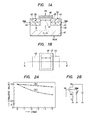
- Figure 1A is a sectional view which shows an example of the device structure of a MOS transistor of small body effect according to the present invention.
- a p-type impurity region 42 (hereinbelow, briefly denoted as "p-well") the impurity concentration of which is 10 15 - 10 16 cm -3 .
- the material of the n-type substrate appears in a partial region 47 of the major surface.
- the n-type region surrounded by the p-well shall be called the "opening".
- FIG. 1B is a plan view of the device shown in Figure 1A, and Figure 1A corresponds to section A - A' in Figure 1B.
- the device illustrated in Figures 1A and 1B is operated with the potential V BB of the p-well 42 fixed at the ground or a negative potential and the potential V SUB of the substrate 41 fixed at a positive potential, so that the well 42 and the substrate 41 are reverse-biased throughout the operation. While a depletion layer 48 is formed between the p-well 42 and the n-type silicon substrate 41 by the reverse bias voltage, it extends to be deeper on the side of the n-type substrate 41 because the impurity concentration of the n-type silicon substrate 41 is lower than that of the p-well 42. The depletion layer 48 is formed within the p-well opening 47 located between the source 43 and the drain 44.
- the width a of the p-well opening 47 is smaller than double the depth d of the depletion layer, namely, 2 ⁇ d
- the interior of the p-well opening 47 underneath the gate is entirely depleted, with the result that a deep depletion layer corresponding to (depth of the p-well 42 + depth d of the depletion layer 48) is formed underneath the gate 4 ⁇ .
- positive charges resulting from the ionization of the donor impurity of the n-type substrate exist within the depletion layer.
- the MOS transistor of the present structure comes to have a negative threshold voltage and be in the depletion mode.
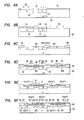
- Figure 2A shows the current characteristic of the device illustrated in Figures 1A and 1B.
- a method of measuring the characteristic is as depicted in Figure 2B. More specifically, variation in current I flowing between the drain and source of the transistor was measured by varying the applied voltage V BB to the p-well 42 with the drain potential V D and the source potential V S held fixed respectively.
- the current I flowing through the device of the embodiment is substantially constant irrespective of the voltage V BB applied to the well, and the body effect is hardly observed.
- a broken line in Figure 2A illustrates an example of the current characteristic of a conventional depletion-mode MOS transistor in which n-type source, drain and channel regions are formed in the major surface of a p-type silicon substrate.
- the threshold voltage of the MOS transistor which determines the device current can be controlled by varying the impurity concentration of the n-type substrate region within the p-well opening.
- the impurity concentration of the n-type substrate region is made higher, the threshold voltage increases in the negative direction, and a greater current flows.
- the depth of the depletion layer 48 extending into the p-well opening 47 is changed by varying the voltage which is applied across the n-type substrate 41 and the p-well 42. Therefore, the characteristic of the device somewhat changes depending upon the magnitude of this voltage.
- Figure 3 shows a plan view of an embodiment which differs from the embodiment of Figures 1A and 1B in the positions of source and drain regions.
- an n + layer 43 to function as the source and an n layer 44 to function as the drain are formed in a manner to partly extend into the opening 47 of the p-well.
- the other points are the same as in Figures 1A and 1B, and a device having substantially the same characteristic is obtained.
- Figure 4 shows still another embodiment.
- an n + layer 43 to function as the source and an n layer 44 to function as the drain are not exposed to the side surfaces of the opening 47 of the p-well, but they are included within the p-well in a manner to stand back from the side surfaces.
- Such a device is liable to be produced by the lateral diffusion of an impurity during the manufacturing process. It exhibits substantially the same characteristic as that of the device of Figures 1A and 1B, subject to the condition that the distance between the opening 47 and the source 43 or the drain 44 is short.
- Figure 5A shows still another embodiment.
- a p-well 70, a source region 73, a drain -region 74, a gate 76, a gate oxide film 77, etc. are formed similarly to those of the example shown in Figure 1A.
- the width a of an opening 71, the impurity concentrations of the respective regions, and the value of the reverse bias voltage (V BB - V SUB ) across the p-well 70 and a substrate 75 are selected so that the opening 71 of the p-well 70 may not be entirely depleted but that an n-type region where conduction electrons exist may be left in the central part thereof.
- the interior of the opening of the p-well is not wholly depleted but the device structure as in the present embodiment is realized, subject to the condition that the width of the p-well opening is at least 10 ⁇ m.
- the impurity concentration of the n-type substrate is made 5 x 10 15 cm -3
- the device structure of the present embodiment is realized subject to the condition that the p-well opening is at least 5 ⁇ m wide.
- this MOS transistor has the characteristic of small body effect in the depletion mode, and the current controlled by the gate voltage flows between the source 73 and the drain 74. Since, however, the p-well opening 71 is not entirely depleted in this device, there is also current which flows from the n-type substrate 75,having a positive potential applied thereto, into the source 73 through the p-well opening 71.
- an equivalent circuit of this MOS transistor is considered such that a depletion-mode MOS transistor 78 as shown in Figure 1A and a vertical junction type FET 79 having an n-channel are connected in parallel, the FET having the n-type substrate 75 as its drain, the p-well 70 as its gate and the n layer 73 as its source.
- the load current flows through the two elements, so that the capability to charge the load capacitance is high and the operating speed of the circuit can be rendered high.
- the present device is cubically formed in such a manner that the vertical junction type FET is buried in under the gate electrode. Therefore, the load current supplying capability relative to the device area is great, and the device is capable of achieving a high density of integration.
- the device of the present embodiment is formed with a p-type well 92 in the major surface of an n-type silicon substrate 91 in a manner to leave an opening 97 behind and is provided with an n" layer 93 to serve as the source, an n + layer 94 to serve as the drain, a gate oxide film 95 and a gate electrode 96.
- the interior of the p-well opening 97 is entirely depleted, but a p-type impurity layer 99 is formed in the surface of the p-well opening 97 underneath the gate electrode 96 by ion implantation.or the like in order to bring the threshold voltage of the transistor into one of the enhancement mode.
- a p-type impurity layer 99 is formed in the surface of the p-well opening 97 underneath the gate electrode 96 by ion implantation.or the like in order to bring the threshold voltage of the transistor into one of the enhancement mode.
- the p-type impurity layer 99 should desirably be made deep at most 0.5 ⁇ m/and as shallow as possible.
- a MOS transistor which has the characteristic of the enhancement mode and whose body effect is suppressed, can also be realized in such a way that, in the structure depicted in Figures 1A and 1B, the gate electrode 46 is formed of a material having a great work function, for example, p-type polycrystalline silicon at a high impurity concentration.
- CMOS circuit complementary MOS transistor circuit
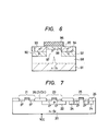
- Figure 7 is a sectional view showing such an example.
- a p-channel MOS transistor 21 is formed on an n-type Si substrate 20 .
- an n-channel MOS transistor 23 of the conventional structure is formed in a p-well 22 within the n-type substrate.
- an n-channel MOS transistor 25 of suppressed body effect which is similar to the transistor of Figures 1A and 1B is formed.
- Numeral 26 designates a thick Si0 2 film for isolating the elements.
- a circuit of high operating speed can be formed by this MCS transistor whose body effect is suppressed.
- a circuit of low power dissipation can be formed by the CMOS circuit.
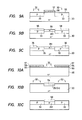
- FIGS 8A to 8F illustrate in detail a method of manufacturing still another embodiment in which the MOS transistor of suppressed body effect according to the present invention is combined with a CMOS circuit.
- a pattern 31 of an SiO 2 film which is 0.5 - 1.0 ⁇ m thick is formed on those areas of the surface of an n-type substrate 30 having an impurity concentration of 10 14 - 10 15 cm -3 which corresponds to the opening of a p-well and under which no well is formed.
- a p-type impurity such as boron 32 is ion-implanted under the condition of an ion dose of 10 12 -10 13 cm -2 .
- the impurity is thermally diffused at a high temperature of 1100 - 1200 °C, to form the p-well 33 which is 3 - 4 ⁇ m deep ( Figure 8A).
- n-type impurity such as phosphorus 35 is ion-implanted into-the p-well opening and the other region than the p-well under the condition of an ion dose of 1 0 11 - 10 13 cm -2 , thereby to set the impurity concentration of the p-well opening as well as the aforementioned other region at a desired value ( Figure 8B).
- a field oxide film 36 having a thickness of 0.5 - 1.0 fm is formed by selective oxidation (Figure 8C).
- the ion-implanted n-type impurity of the p-well opening etc. diffuses by approximately 0.5 - 1.5 fm as indicated at numeral 351 ( Figure 8C).
- a thin gate oxide film 37 having a thickness of 20 - 100 nm and gate electrodes 38 made of polycrystalline silicon or a metal are formed.
- the surface part is doped with a p-type impurity such as boron by the ion implantation or the like before the gate electrodes 38 are formed.
- a mask 39 such as a photoresist film, SiO 2 film and Si 3 N 4 film, whereupon the n + regions 50 are formed by the use of phosphorus or arsenic ( Figure 8D).
- the mask 39 is removed.
- a mask 51 such as a photoresist film, SiO 2 film and Si 3 N 4 film again, high concentration p + regions 52 are formed ( Figure 8E).
- the p + regions become a region for leading out an electrode from the p-well, and also the source and drain of a p-channel transistor for constructing the CMOS circuit.
- a surface protective film 53 such as a PSG film is formed, electrode holes are provided, and electrodes 5A are formed. Then, the device is prepared for use in the usual way.
- Figures 9A - 9C illustrate another process which is employed instead of the process for forming the p-well and doping the p-well opening with the n-type impurity as explained with reference to Figures 8A - 8C.
- a pattern consisting of an Si 3 N 4 film 56 and a photoresist film 57 is formed on that area of the surface of the n-type silicon substrate 30 which corresponds to the opening to be formed, through an Si0 2 film 55 having a thickness of 20 - 100 nm.
- the p-type impurity 32 is ion-implanted, whereupon it is thermally diffused to form the p-well 33 ( Figure 9A).
- the n-type impurity of the p-well opening is diffused tc be 0.5 - 1.5 ⁇ m deep, so that the n-type region 351 is formed.
- the n + regions are formed by a process similar to that explained with reference to Figures 8D, 8E and 8F. Then, the MOS transistor is completed for use.
- Figures 10A - 10C illustrate still another process for forming the p-well and the n-type impurity layer within the p-well opening.
- an SiO 2 film 55, an S i 3N4 film 56 and a photoresist film 57 which are 20 - 100 nm thick are stacked on the substrate 30.
- the Si 3 N 4 film 56 and the photoresist film 57 in an area corresponding to the p-well opening to be formed are removed, and the n-type impurity 35 is ion-implanted (Figure 10A).
- the MOS transistors of small body effect can be achieved in accordance with the present invention. Any of these transistors can produce the load current of the constant current characteristic which hardly changes even when the source potential has changed. Therefore, when applied to various parts of integrated circuits, the MOS transistors can provide integrated circuits of high operating speed. In general, they are used as loads for deriving outputs from logic networks.
- Figure 11A typically illustrates an example in which the MOS transistor is applied to an inverter circuit.
- the source - gate common end of a depletion-mode MOS transistor 61 of small body effect as illustrated in Figure 1A is connected to the drain of an enhancement-mode MOS transistor 62 whose source is earthed. The connection point is used as an output terminal, while the gate of the enhancement-mode MOS transistor 62 is used as an input terminal.
- a positive voltage source V CC is connected to the drain of the depletion-mode MOS transistor 61.
- the depletion-mode MOS transistor 61 is disposed at the position of a p-well 63 having an opening.
- the enhancement-mode MOS transistor 62 is disposed in a p-well 64 formed simultaneously with the p-well 63.
- the voltage source V CC is connected to an n-type substrate 60, and both the p-wells 63 and 64 are grounded.
- the MOS transistor 61 employed in the present example allows a load current I L to flow which is substantially constant even when the output voltage V Out' namely, the source potential of the MOS transistor 61 rises. Therefore, the load capacitance is rapidly charged.
- FIG 11C Shown in Figure 11C is a circuit diagram of an E/D MOS inverter circuit in which the aforementioned depletion-mode MOS transistor 61 is replaced with a depletion-mode MOS transistor 61' as shown in Figure 5A. With this MOS transistor 61', charging current flows also from the n-type substrate 60 to the load through the p-well opening, so that an inverter circuit of faster operation can be realized.
- the inverter circuits In the above, two examples of the inverter circuits have been described. Generally speaking, it is a logic network that is connected in the place of the enhancement-mode MOS transistor 62.
- the depletion-mode MOS transistor 61 or 61' is driven by the logic network as the load thereof, and output signals of high speed can be provided from the output terminal.
- Figure 12 shows an example in which the MOS transistor of the present invention is applied to a transfer gate.
- the MOS transistor of the present invention as shown in Figure 1A is employed for each of the transfer gates T1 and T2 of a memory cell in a static MOS-RAM.
- symbol V CC denotes a power source line
- symbol W a word line
- symbols D and D data lines symbols
- symbols R1 and R2 resistors symbols
- symbols S1 and S2 switching MOS transistors symbols.
Landscapes
- Engineering & Computer Science (AREA)
- Power Engineering (AREA)
- Microelectronics & Electronic Packaging (AREA)
- Physics & Mathematics (AREA)
- Condensed Matter Physics & Semiconductors (AREA)
- General Physics & Mathematics (AREA)
- Computer Hardware Design (AREA)
- Ceramic Engineering (AREA)
- Manufacturing & Machinery (AREA)
- Metal-Oxide And Bipolar Metal-Oxide Semiconductor Integrated Circuits (AREA)
Applications Claiming Priority (2)
| Application Number | Priority Date | Filing Date | Title |
|---|---|---|---|
| JP113692/81 | 1981-07-22 | ||
| JP56113692A JPS5816565A (ja) | 1981-07-22 | 1981-07-22 | 絶縁ゲ−ト形電界効果トランジスタ |
Publications (3)
| Publication Number | Publication Date |
|---|---|
| EP0070744A2 true EP0070744A2 (fr) | 1983-01-26 |
| EP0070744A3 EP0070744A3 (en) | 1983-10-05 |
| EP0070744B1 EP0070744B1 (fr) | 1986-03-26 |
Family
ID=14618761
Family Applications (1)
| Application Number | Title | Priority Date | Filing Date |
|---|---|---|---|
| EP82303890A Expired EP0070744B1 (fr) | 1981-07-22 | 1982-07-22 | Transistor à effet de champ à porte isolée |
Country Status (5)
| Country | Link |
|---|---|
| EP (1) | EP0070744B1 (fr) |
| JP (1) | JPS5816565A (fr) |
| KR (1) | KR840000988A (fr) |
| CA (1) | CA1189637A (fr) |
| DE (1) | DE3270103D1 (fr) |
Cited By (9)
| Publication number | Priority date | Publication date | Assignee | Title |
|---|---|---|---|---|
| WO1990010309A2 (fr) * | 1989-03-02 | 1990-09-07 | Thunderbird Technologies Inc. | Transistor a effet de champ a seuil de fermi |
| US4990974A (en) * | 1989-03-02 | 1991-02-05 | Thunderbird Technologies, Inc. | Fermi threshold field effect transistor |
| US5367186A (en) * | 1992-01-28 | 1994-11-22 | Thunderbird Technologies, Inc. | Bounded tub fermi threshold field effect transistor |
| US5369295A (en) * | 1992-01-28 | 1994-11-29 | Thunderbird Technologies, Inc. | Fermi threshold field effect transistor with reduced gate and diffusion capacitance |
| US5440160A (en) * | 1992-01-28 | 1995-08-08 | Thunderbird Technologies, Inc. | High saturation current, low leakage current fermi threshold field effect transistor |
| US5525822A (en) * | 1991-01-28 | 1996-06-11 | Thunderbird Technologies, Inc. | Fermi threshold field effect transistor including doping gradient regions |
| US5543654A (en) * | 1992-01-28 | 1996-08-06 | Thunderbird Technologies, Inc. | Contoured-tub fermi-threshold field effect transistor and method of forming same |
| US5786620A (en) * | 1992-01-28 | 1998-07-28 | Thunderbird Technologies, Inc. | Fermi-threshold field effect transistors including source/drain pocket implants and methods of fabricating same |
| US5814869A (en) * | 1992-01-28 | 1998-09-29 | Thunderbird Technologies, Inc. | Short channel fermi-threshold field effect transistors |
Families Citing this family (1)
| Publication number | Priority date | Publication date | Assignee | Title |
|---|---|---|---|---|
| JP4846239B2 (ja) * | 2002-12-13 | 2011-12-28 | エイチアールエル ラボラトリーズ,エルエルシー | ウェル注入を用いた集積回路の改変 |
Citations (5)
| Publication number | Priority date | Publication date | Assignee | Title |
|---|---|---|---|---|
| US3615938A (en) * | 1969-01-28 | 1971-10-26 | Westinghouse Electric Corp | Method for diffusion of acceptor impurities into semiconductors |
| US3916430A (en) * | 1973-03-14 | 1975-10-28 | Rca Corp | System for eliminating substrate bias effect in field effect transistor circuits |
| US3983620A (en) * | 1975-05-08 | 1976-10-05 | National Semiconductor Corporation | Self-aligned CMOS process for bulk silicon and insulating substrate device |
| US4039869A (en) * | 1975-11-28 | 1977-08-02 | Rca Corporation | Protection circuit |
| EP0006428A2 (fr) * | 1978-06-30 | 1980-01-09 | International Business Machines Corporation | Dispositif semiconducteur à tension de seuil constante |
-
1981
- 1981-07-22 JP JP56113692A patent/JPS5816565A/ja active Pending
-
1982
- 1982-07-21 KR KR1019820003261A patent/KR840000988A/ko unknown
- 1982-07-22 CA CA000407812A patent/CA1189637A/fr not_active Expired
- 1982-07-22 DE DE8282303890T patent/DE3270103D1/de not_active Expired
- 1982-07-22 EP EP82303890A patent/EP0070744B1/fr not_active Expired
Patent Citations (5)
| Publication number | Priority date | Publication date | Assignee | Title |
|---|---|---|---|---|
| US3615938A (en) * | 1969-01-28 | 1971-10-26 | Westinghouse Electric Corp | Method for diffusion of acceptor impurities into semiconductors |
| US3916430A (en) * | 1973-03-14 | 1975-10-28 | Rca Corp | System for eliminating substrate bias effect in field effect transistor circuits |
| US3983620A (en) * | 1975-05-08 | 1976-10-05 | National Semiconductor Corporation | Self-aligned CMOS process for bulk silicon and insulating substrate device |
| US4039869A (en) * | 1975-11-28 | 1977-08-02 | Rca Corporation | Protection circuit |
| EP0006428A2 (fr) * | 1978-06-30 | 1980-01-09 | International Business Machines Corporation | Dispositif semiconducteur à tension de seuil constante |
Non-Patent Citations (1)
| Title |
|---|
| IBM Technical Disclosure Bulletin, vol. 6, no. 9, Febr. 1964, pages 91-93 * |
Cited By (12)
| Publication number | Priority date | Publication date | Assignee | Title |
|---|---|---|---|---|
| WO1990010309A2 (fr) * | 1989-03-02 | 1990-09-07 | Thunderbird Technologies Inc. | Transistor a effet de champ a seuil de fermi |
| WO1990010309A3 (fr) * | 1989-03-02 | 1991-01-24 | Thunderbird Tech Inc | Transistor a effet de champ a seuil de fermi |
| US4990974A (en) * | 1989-03-02 | 1991-02-05 | Thunderbird Technologies, Inc. | Fermi threshold field effect transistor |
| US5151759A (en) * | 1989-03-02 | 1992-09-29 | Thunderbird Technologies, Inc. | Fermi threshold silicon-on-insulator field effect transistor |
| US5525822A (en) * | 1991-01-28 | 1996-06-11 | Thunderbird Technologies, Inc. | Fermi threshold field effect transistor including doping gradient regions |
| US5367186A (en) * | 1992-01-28 | 1994-11-22 | Thunderbird Technologies, Inc. | Bounded tub fermi threshold field effect transistor |
| US5369295A (en) * | 1992-01-28 | 1994-11-29 | Thunderbird Technologies, Inc. | Fermi threshold field effect transistor with reduced gate and diffusion capacitance |
| US5374836A (en) * | 1992-01-28 | 1994-12-20 | Thunderbird Technologies, Inc. | High current fermi threshold field effect transistor |
| US5440160A (en) * | 1992-01-28 | 1995-08-08 | Thunderbird Technologies, Inc. | High saturation current, low leakage current fermi threshold field effect transistor |
| US5543654A (en) * | 1992-01-28 | 1996-08-06 | Thunderbird Technologies, Inc. | Contoured-tub fermi-threshold field effect transistor and method of forming same |
| US5786620A (en) * | 1992-01-28 | 1998-07-28 | Thunderbird Technologies, Inc. | Fermi-threshold field effect transistors including source/drain pocket implants and methods of fabricating same |
| US5814869A (en) * | 1992-01-28 | 1998-09-29 | Thunderbird Technologies, Inc. | Short channel fermi-threshold field effect transistors |
Also Published As
| Publication number | Publication date |
|---|---|
| EP0070744B1 (fr) | 1986-03-26 |
| DE3270103D1 (en) | 1986-04-30 |
| JPS5816565A (ja) | 1983-01-31 |
| EP0070744A3 (en) | 1983-10-05 |
| CA1189637A (fr) | 1985-06-25 |
| KR840000988A (ko) | 1984-03-26 |
Similar Documents
| Publication | Publication Date | Title |
|---|---|---|
| US4209797A (en) | Complementary semiconductor device | |
| US4703552A (en) | Fabricating a CMOS transistor having low threshold voltages using self-aligned silicide polysilicon gates and silicide interconnect regions | |
| US5266507A (en) | Method of fabricating an offset dual gate thin film field effect transistor | |
| EP0952614B1 (fr) | Dispositif à effet de champ avec un canal en silicium polycristallin | |
| US6110773A (en) | Static random access memory device manufacturing method | |
| US4893164A (en) | Complementary semiconductor device having high switching speed and latchup-free capability | |
| GB1563863A (en) | Igfet inverters and methods of fabrication thereof | |
| JP3470133B2 (ja) | 半導体装置の製造方法 | |
| US4131907A (en) | Short-channel V-groove complementary MOS device | |
| EP0070744B1 (fr) | Transistor à effet de champ à porte isolée | |
| US4907059A (en) | Semiconductor bipolar-CMOS inverter | |
| US4484209A (en) | SOS Mosfet with thinned channel contact region | |
| US5945715A (en) | Semiconductor memory device having a memory cell region and a peripheral circuit region and method of manufacturing the same | |
| US4384300A (en) | Negative resistance device | |
| US6635518B2 (en) | SOI FET and method for creating FET body connections with high-quality matching characteristics and no area penalty for partially depleted SOI technologies | |
| US5016077A (en) | Insulated gate type semiconductor device and method of manufacturing the same | |
| EP0054471B1 (fr) | Elément de résistance semiconducteur | |
| US4476479A (en) | Semiconductor device with operating voltage coupling region | |
| EP0263287A2 (fr) | Fabrication d'un capaciteur dans un circuit intégré | |
| GB2342778A (en) | Semiconductor memory devices | |
| KR0183485B1 (ko) | 반도체 디바이스 및 그 제조 방법 | |
| US4679298A (en) | Method of fabrication of GaAs complementary enhancement mode junction field effect transistor | |
| US6232195B1 (en) | Structure of semiconductor device | |
| JP2550119B2 (ja) | 半導体記憶装置 | |
| US5027186A (en) | Semiconductor device |
Legal Events
| Date | Code | Title | Description |
|---|---|---|---|
| PUAI | Public reference made under article 153(3) epc to a published international application that has entered the european phase |
Free format text: ORIGINAL CODE: 0009012 |
|
| 17P | Request for examination filed |
Effective date: 19820907 |
|
| AK | Designated contracting states |
Designated state(s): DE FR GB NL |
|
| PUAL | Search report despatched |
Free format text: ORIGINAL CODE: 0009013 |
|
| AK | Designated contracting states |
Designated state(s): DE FR GB NL |
|
| GRAA | (expected) grant |
Free format text: ORIGINAL CODE: 0009210 |
|
| AK | Designated contracting states |
Kind code of ref document: B1 Designated state(s): DE FR GB NL |
|
| REF | Corresponds to: |
Ref document number: 3270103 Country of ref document: DE Date of ref document: 19860430 |
|
| ET | Fr: translation filed | ||
| PLBE | No opposition filed within time limit |
Free format text: ORIGINAL CODE: 0009261 |
|
| STAA | Information on the status of an ep patent application or granted ep patent |
Free format text: STATUS: NO OPPOSITION FILED WITHIN TIME LIMIT |
|
| 26N | No opposition filed | ||
| PGFP | Annual fee paid to national office [announced via postgrant information from national office to epo] |
Ref country code: NL Payment date: 19870731 Year of fee payment: 6 |
|
| PG25 | Lapsed in a contracting state [announced via postgrant information from national office to epo] |
Ref country code: NL Effective date: 19890201 |
|
| NLV4 | Nl: lapsed or anulled due to non-payment of the annual fee | ||
| PG25 | Lapsed in a contracting state [announced via postgrant information from national office to epo] |
Ref country code: DE Effective date: 19890401 |
|
| PG25 | Lapsed in a contracting state [announced via postgrant information from national office to epo] |
Ref country code: GB Effective date: 19890722 |
|
| GBPC | Gb: european patent ceased through non-payment of renewal fee | ||
| PG25 | Lapsed in a contracting state [announced via postgrant information from national office to epo] |
Ref country code: FR Free format text: LAPSE BECAUSE OF NON-PAYMENT OF DUE FEES Effective date: 19900330 |
|
| REG | Reference to a national code |
Ref country code: FR Ref legal event code: ST |