EP0068949B1 - Procédé et dispositif optique de conversion analogique-numérique - Google Patents
Procédé et dispositif optique de conversion analogique-numérique Download PDFInfo
- Publication number
- EP0068949B1 EP0068949B1 EP82401043A EP82401043A EP0068949B1 EP 0068949 B1 EP0068949 B1 EP 0068949B1 EP 82401043 A EP82401043 A EP 82401043A EP 82401043 A EP82401043 A EP 82401043A EP 0068949 B1 EP0068949 B1 EP 0068949B1
- Authority
- EP
- European Patent Office
- Prior art keywords
- channel
- arms
- interferometer
- substrate
- electrodes
- Prior art date
- Legal status (The legal status is an assumption and is not a legal conclusion. Google has not performed a legal analysis and makes no representation as to the accuracy of the status listed.)
- Expired
Links
- 230000003287 optical effect Effects 0.000 title claims description 20
- 238000000034 method Methods 0.000 title claims description 12
- 238000006243 chemical reaction Methods 0.000 title claims description 5
- 230000010363 phase shift Effects 0.000 claims description 32
- 239000000758 substrate Substances 0.000 claims description 20
- 230000005684 electric field Effects 0.000 claims description 7
- GQYHUHYESMUTHG-UHFFFAOYSA-N lithium niobate Chemical compound [Li+].[O-][Nb](=O)=O GQYHUHYESMUTHG-UHFFFAOYSA-N 0.000 claims description 5
- 238000009792 diffusion process Methods 0.000 claims description 3
- 239000000463 material Substances 0.000 claims description 3
- 230000005855 radiation Effects 0.000 claims description 3
- RTAQQCXQSZGOHL-UHFFFAOYSA-N Titanium Chemical compound [Ti] RTAQQCXQSZGOHL-UHFFFAOYSA-N 0.000 claims description 2
- 238000001514 detection method Methods 0.000 claims description 2
- 229910052719 titanium Inorganic materials 0.000 claims description 2
- 239000010936 titanium Substances 0.000 claims description 2
- 238000010586 diagram Methods 0.000 description 6
- 230000004044 response Effects 0.000 description 4
- 230000007704 transition Effects 0.000 description 3
- 230000007423 decrease Effects 0.000 description 2
- 230000004048 modification Effects 0.000 description 2
- 238000012986 modification Methods 0.000 description 2
- 230000008569 process Effects 0.000 description 2
- 238000010200 validation analysis Methods 0.000 description 2
- WSMQKESQZFQMFW-UHFFFAOYSA-N 5-methyl-pyrazole-3-carboxylic acid Chemical compound CC1=CC(C(O)=O)=NN1 WSMQKESQZFQMFW-UHFFFAOYSA-N 0.000 description 1
- JBRZTFJDHDCESZ-UHFFFAOYSA-N AsGa Chemical compound [As]#[Ga] JBRZTFJDHDCESZ-UHFFFAOYSA-N 0.000 description 1
- 230000015556 catabolic process Effects 0.000 description 1
- 230000000295 complement effect Effects 0.000 description 1
- 238000010276 construction Methods 0.000 description 1
- 230000008878 coupling Effects 0.000 description 1
- 238000010168 coupling process Methods 0.000 description 1
- 238000005859 coupling reaction Methods 0.000 description 1
- 238000004519 manufacturing process Methods 0.000 description 1
- 230000005693 optoelectronics Effects 0.000 description 1
- 238000000206 photolithography Methods 0.000 description 1
- 230000000135 prohibitive effect Effects 0.000 description 1
- 238000005070 sampling Methods 0.000 description 1
- 230000035945 sensitivity Effects 0.000 description 1
Images


Classifications
-
- H—ELECTRICITY
- H03—ELECTRONIC CIRCUITRY
- H03M—CODING; DECODING; CODE CONVERSION IN GENERAL
- H03M1/00—Analogue/digital conversion; Digital/analogue conversion
- H03M1/12—Analogue/digital converters
- H03M1/34—Analogue value compared with reference values
- H03M1/36—Analogue value compared with reference values simultaneously only, i.e. parallel type
- H03M1/361—Analogue value compared with reference values simultaneously only, i.e. parallel type having a separate comparator and reference value for each quantisation level, i.e. full flash converter type
-
- G—PHYSICS
- G02—OPTICS
- G02F—OPTICAL DEVICES OR ARRANGEMENTS FOR THE CONTROL OF LIGHT BY MODIFICATION OF THE OPTICAL PROPERTIES OF THE MEDIA OF THE ELEMENTS INVOLVED THEREIN; NON-LINEAR OPTICS; FREQUENCY-CHANGING OF LIGHT; OPTICAL LOGIC ELEMENTS; OPTICAL ANALOGUE/DIGITAL CONVERTERS
- G02F7/00—Optical analogue/digital converters
Definitions
- the present invention relates to a method and an optical device for analog-digital conversion.
- the method of the invention which uses the properties of the integrated optical amplitude modulator does not have this limit.
- the subject of the invention is an optical process for analog-digital conversion in an encoder comprising n channels corresponding to the n binary elements of the digital output word, each channel comprising at least one light intensity modulator comprising on the surface of a substrate.
- the invention further relates to a device implementing this method.
- FIG. 1 The structure of the analog-digital encoder produced in integrated optics of the known art is shown in FIG. 1. It is produced from basic elements comprising a light intensity modulator produced with a two-arm interferometer.
- a light wave 11 produced by a laser source is presented at the input of this device which has six channels each comprising an elementary optical modulator integrated on a substrate 10. Each modulator therefore corresponds to a binary element of the output word.
- the signal to be digitized S (t) is applied to electrodes belonging to each of these elementary optical modulators.
- the length of these electrodes is different.
- L for the modulator of channel 1, and L 2 .
- bias voltages which we will call V lbiais applied to the modulators of these different channels; these voltages making it possible to introduce a fixed phase shift or "bias" on an arm.
- AND gates 14 allow validation of the output signal at a certain time. This validation can take into account the transit time in these modulators; when using, for example, at input 11 a pulsed laser, this allows sampling over time. A binary word is thus obtained in parallel.
- the response time of such an analog-digital encoder has been measured, it is less than 0.5 nanosecond.
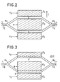
- FIG. 2 the diagram of such a two-arm interferometer for modulating the light intensity I E.
- This interferometer comprises a branch of a single-mode input waveguide 1 in which a light wave of intensity I E is coupled.
- This branch 1 separates at the bifurcation B 1 into two parallel arms 2 and 3 constituting single-mode guides, which join in a bifurcation B z to form a branch of a single-mode output waveguide 4 from which a intensity I S.
- the directions of propagation in the four guides are the same.
- this two-arm interferometer has two outputs. Indeed, when the signals are in phase opposition, the light propagates inside the substrate; which amounts to exciting the higher mode which does not propagate in the guide but which leaks in the substrate.
- Electrodes are arranged on either side of each of the guides 2 and 3, for example a central electrode E o , an electrode E 2 on the other side of the arm 2 and to which a voltage V 2 and an electrode are applied Eg on the other side of the arm 3 to which a voltage V 3 is applied, the electrode E o being connected to ground.
- the arrangement of the electrodes as shown in FIG. 2, that is to say not covering the guides but being adjacent to them, causes in each of the guides 2 and 3 electric fields perpendicular to the direction of propagation of the light waves and in the plane of the figure.
- the propagation mode used in the guides is a TE mode.
- the entire device is produced on the surface of a substrate having electrooptical properties, such as lithium niobate (LiNb0 3 ), lithium tantalate (LiTaO 3 ) or gallium arsenide (GaAs).
- a substrate having electrooptical properties such as lithium niobate (LiNb0 3 ), lithium tantalate (LiTaO 3 ) or gallium arsenide (GaAs).
- the optical waveguides are obtained by diffusion of titanium. This diffusion is selective thanks to conventional photolithography processes.
- the axis c of the lithium niobate is also in this plane and perpendicular to the direction of propagation common to the guides 1 to 4, so as to present the maximum electrooptical effect.
- the fields cause variations in the propagation speeds of the light waves for each of the two guides: the voltage V 3 causes a variation in opposite direction - ⁇ ⁇ 2 which is also its proportional. These speed variations cause at the location of the bifurcation B 2 a phase difference between the two waves coming from the guides 2 and 3 which were originally in phase at the bifurcation B i .
- This phase shift ⁇ ⁇ is equal to ⁇ ⁇ 3 L 3 + ⁇ ⁇ 2 L 2 where L 2 and L 3 are the lengths of the electrodes between the two bifurcations B 1 and B 2 .
- FIG. 3 also represents the diagram of a two-arm interferometer. But this time the electrodes E 3 and E o are deposited on the surface of the substrate above the two guides 2 and 3. The arrangement of these electrodes causes in each of these guides 2 and 3 fields perpendicular to the propagation of the light waves, and perpendicular to the plane of the figure. It is preferable then that the axis C of the lithium niobate is also perpendicular to the direction of propagation common to the guides 1 to 4, and perpendicular to the plane of the figure.
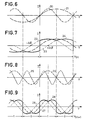
- FIG. 4 is the curve representative of the emerging intensity I s relating to the two types of interferometer shown in FIGS. 2 and 3, as a function of the phase shift ⁇ ⁇ existing at the location of the bifurcation 8 2 , or of the voltage V equal to the voltage (or the sum of the voltages) applied to at least one of the electrodes E 2 and E o , taken with its (their) sign relative to the ground.
- V is zero
- the output intensity I s is maximum and is equal to I SM .
- V is zero
- the output intensity I s is maximum and is equal to I SM .
- each arm of the interferometer can also be subjected to a modulating field originating from a first voltage V M while the other part is subjected to a modulating field coming from a second voltage V R.
- V M first voltage
- V R second voltage
- the invention relates to an analog-digital encoder of the same structure as that illustrated in FIG. 1 using as a basic element the integrated optical amplitude modulator as described above.
- the method used makes it possible to overcome the problem mentioned above, namely the removal of ambiguity.
- the corresponding output signals presented pass through their average level simultaneously every other time as shown in FIG. 6.
- the additional phase shift ⁇ is such that ⁇ / ⁇ -rr / 2.
- the successive positive half-waves of the signal 20 corresponding to the binary element i + 1 fall in phase with the positive and then negative half-waves of the signal 22 which is part of the resulting signal 24 drawn in strong lines.
- the successive negative half-waves of the signal corresponding to the binary element i + 1 are in phase or in opposition to phase with the positive or negative alternations of the signal 23 which is a part of the resulting signal 24 drawn in strong lines. This way of proceeding makes it possible to force the decision.
- the signal 26 corresponding to the previous signal 22 and the signal 27 corresponding to the previous signal 23 are obtained.
- the signals 22 or 26 which are offset by - ⁇ relative to the signal representing the i or i + 1: signal B, and the signals 23 or 27 offset by + ⁇ : signal A will be called generally thereafter.
- the integrated optical circuit corresponding to a binary element of the output word can be envisaged.
- the basic element remains the integrated optical amplitude modulator on the electrodes of which the signal to be digitized is applied plus a complementary voltage ensuring phase shifts of + ⁇ or - ⁇ , ⁇ being equal for example to ⁇ / 4.
- bias voltages V ibia can also exist as in the case illustrated in FIG. 5, bias voltages V ibiais to compensate for the differences existing between the optical paths, or to introduce additional phase shifts such as in the case of using the Gray code.
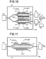
- a first embodiment is shown in Figure 10: the radiation from the laser is coupled simultaneously in two identical modulators.
- the voltage applied to the electrodes of the first (of the second) is the voltage to be digitized plus a voltage ensuring an additional phase shift of + ⁇ (from - ⁇ ).
- the first modulator generates the signal A, the second the signal B.
- the outputs A and B corresponding to the two channels are switched at 31 by a logic signal coming from the stage i + 1 represented at 32.
- the photodetectors followed by comparators are represented in 29 and 30.
- a second embodiment illustrated in FIG. 11 consists in using only one amplitude modulator on the electrodes from which, in addition to the voltage to be digitized, is applied a voltage ensuring a phase shift of + ⁇ or - ⁇ according to l information given by stage i + 1, the photodetector followed by the comparator is shown at 44.
- the n bits of the output word are available in parallel.
- the different binary elements are known one after the other, the most significant binary element being known last.
- the fact that the response for the binary element i, requires knowing the bit (i + 1) means that the total response time is n nanoseconds for a coder with n binary elements is of the order of 6 nanoseconds for an encoder of 6 binary elements of the output word, and this transit time is not prohibitive for most applications.
- FIG. 12 A modification of the circuit, corresponding to the least significant binary element, is illustrated in FIG. 12. It makes it possible to add two additional binary elements of precision. Indeed one can thus obtain the signals A. B, - A, - B; - A and - B being the signals in phase opposition with the signals A and B. We obtain additional information from the dial in which the sinusoid is located. By transcoding we obtain two binary elements of the output word. One Sn + 1 corresponding to the comparison of A and B and the other Sn + 2 to the comparison of A and - B as shown in Figure 13.
- FIG 12 corresponds to figure 10 to which some modifications have been made.
- the circuits 50 and 51 make it possible to obtain the signals - A and - B.
- At the output of the circuit 52 we have the signals A, B, - A, - B and at the output of the circuit 53 we have the signals corresponding to the two binary elements additional: Sn + 1 and Sn + 2.
- FIG. 14 represents a concrete embodiment of the device previously described and illustrated in FIG. 10.
- the signal V if + 1 from the binary element i + 1 is either 0 if the binary element is 0, or V if the binary element is 1. It is sent to a comparator 56 on which a reference voltage is entered V ref1 .
- V i + 1 ⁇ V ref1 V s ⁇ 0 ⁇ the voltage VA applied to the electrode of 41 is little different from 0: VA - 0 ⁇ zero phase shift.
- V i + 1 V ref1 V s ⁇ 0 ⁇ the voltage VA applied to the electrode 41 is such that the phase shift is 2 ⁇ .
Landscapes
- Physics & Mathematics (AREA)
- Engineering & Computer Science (AREA)
- Theoretical Computer Science (AREA)
- General Physics & Mathematics (AREA)
- Nonlinear Science (AREA)
- Optics & Photonics (AREA)
- Optical Modulation, Optical Deflection, Nonlinear Optics, Optical Demodulation, Optical Logic Elements (AREA)
- Instruments For Measurement Of Length By Optical Means (AREA)
- Analogue/Digital Conversion (AREA)
Applications Claiming Priority (2)
| Application Number | Priority Date | Filing Date | Title |
|---|---|---|---|
| FR8112614A FR2508659A1 (fr) | 1981-06-26 | 1981-06-26 | Procede et dipositif optique de conversion analogique-numerique |
| FR8112614 | 1981-06-26 |
Publications (2)
| Publication Number | Publication Date |
|---|---|
| EP0068949A1 EP0068949A1 (fr) | 1983-01-05 |
| EP0068949B1 true EP0068949B1 (fr) | 1985-10-09 |
Family
ID=9259918
Family Applications (1)
| Application Number | Title | Priority Date | Filing Date |
|---|---|---|---|
| EP82401043A Expired EP0068949B1 (fr) | 1981-06-26 | 1982-06-08 | Procédé et dispositif optique de conversion analogique-numérique |
Country Status (5)
| Country | Link |
|---|---|
| US (1) | US4502037A (enExample) |
| EP (1) | EP0068949B1 (enExample) |
| JP (1) | JPS587128A (enExample) |
| DE (1) | DE3266782D1 (enExample) |
| FR (1) | FR2508659A1 (enExample) |
Families Citing this family (42)
| Publication number | Priority date | Publication date | Assignee | Title |
|---|---|---|---|---|
| JPH0616145B2 (ja) * | 1983-08-03 | 1994-03-02 | 松下電器産業株式会社 | 光a/d変換装置 |
| US4763973A (en) * | 1985-02-27 | 1988-08-16 | Omron Tateisi Electronics Co. | Waveguide-type optical sensor |
| US4926177A (en) * | 1987-05-21 | 1990-05-15 | Canon Kabushiki Kaisha | Optical analog-digital converter provided with a nonlinear optical element and an optical feedback system for the output lights of said element |
| US4768848A (en) * | 1987-05-29 | 1988-09-06 | Westinghouse Electric Corp. | Fiber optic repeater |
| US4878724A (en) * | 1987-07-30 | 1989-11-07 | Trw Inc. | Electrooptically tunable phase-locked laser array |
| US4866698A (en) * | 1987-11-17 | 1989-09-12 | The Boeing Company | Multiplexed optical communication system |
| GB2213298B (en) * | 1987-11-30 | 1991-05-29 | Plessey Co Plc | Analogue-to-digital converter |
| JPH01223837A (ja) * | 1988-03-03 | 1989-09-06 | Nec Corp | 光多値送信機 |
| US4882775A (en) * | 1988-07-22 | 1989-11-21 | The Boeing Company | Demodulation technique for coherence multiplexed optical data transmission system |
| US4860279A (en) * | 1988-11-30 | 1989-08-22 | The Boeing Company | Source modulated coherence multiplexed optical signal transmission system |
| US4991920A (en) * | 1988-12-27 | 1991-02-12 | Andrzej Peczalski | Optical converter |
| US5010346A (en) * | 1989-10-27 | 1991-04-23 | The Boeing Company | Electro-optical analog-to-digital converter and method for digitizing an analog signal |
| US5239401A (en) * | 1990-12-31 | 1993-08-24 | Gte Laboratories Incorporated | Optical modulator for cancellation of second-order intermodulation products in lightwave systems |
| US5301058A (en) * | 1990-12-31 | 1994-04-05 | Gte Laboratories Incorporated | Single sideband optical modulator for lightwave systems |
| US5142285A (en) * | 1991-02-13 | 1992-08-25 | City College Of New York | Acousto-optic theta modulation-based analog-to-digital converter |
| US5233673A (en) * | 1991-10-09 | 1993-08-03 | Hughes Aircraft Company | Output steerable optical phased array |
| US5237629A (en) * | 1992-03-19 | 1993-08-17 | The United States Of America As Represented By The United States Department Of Energy | Digitally controlled distributed phase shifter |
| DE4216065C2 (de) * | 1992-05-15 | 2002-01-03 | Daimlerchrysler Aerospace Ag | Verfahren zur Analog/Digitalwandlung von Mikrowellensignalen |
| RU2117323C1 (ru) * | 1994-07-27 | 1998-08-10 | Ростовское высшее военное командно-инженерное училище ракетных войск им.Главного Маршала артиллерии Неделина М.И. | Оптический аналого-цифровой преобразователь |
| FR2723277B1 (fr) * | 1994-07-29 | 1996-09-13 | Thomson Csf | Convertisseur analogique-numerique et systeme de conversion analogique-numerique mettant en oeuvre ledit convertisseur |
| US5644665A (en) * | 1995-07-27 | 1997-07-01 | The United States Of America As Represented By The Secretary Of The Navy | Multi-octave, high dynamic range operation of low-biased modulators by balanced detection |
| US6118397A (en) * | 1998-06-17 | 2000-09-12 | Trw Inc. | Fully optical analog to digital converters with complementary outputs |
| US6100831A (en) * | 1998-06-30 | 2000-08-08 | The United States Of America As Represented By The Secretary Of The Navy | Optoelectronic analog-to-digital converter using wavelength division multiplexing |
| US6188342B1 (en) | 1998-11-02 | 2001-02-13 | Tracor Aerospace Electronic Systems, Inc. | Photonic A/D converter using parallel synchronous quantization of optical signals |
| US6246350B1 (en) * | 1998-12-23 | 2001-06-12 | Hughes Electronics Corporation | Optoelectronic analog-to-digital converter |
| US6469649B1 (en) | 2000-03-08 | 2002-10-22 | Massachusetts Institute Of Technology | Narrowband analog to digital converter with suppressed second-order distortion |
| RU2177164C1 (ru) * | 2000-05-24 | 2001-12-20 | Ростовский военный институт ракетных войск | Оптический преобразователь кодов |
| US6404366B1 (en) | 2000-12-01 | 2002-06-11 | The United States Of America As Represented By The Secretary Of The Navy | Photonic analog-to-digital converter utilizing wavelength division multiplexing and distributed optical phase modulation |
| GB2408811B (en) * | 2003-12-06 | 2005-11-23 | Bookham Technology Plc | Optical Modulator |
| CN1297850C (zh) * | 2003-12-25 | 2007-01-31 | 电子科技大学 | 一种集成光学m-z结构模数转换器 |
| JP2008039859A (ja) * | 2006-08-01 | 2008-02-21 | Fujitsu Ltd | 光変調器 |
| US8028755B2 (en) * | 2007-12-14 | 2011-10-04 | Clearwater International Llc | Quick lock wireline valve/blow-out preventor and methods for making and using same |
| RU2371747C1 (ru) * | 2008-02-26 | 2009-10-27 | Сергей Викторович Соколов | Оптический аналого-цифровой нанопреобразователь |
| US7990299B2 (en) * | 2009-08-19 | 2011-08-02 | The Boeing Company | Optical sampling method for analog to digital conversion |
| US8238017B2 (en) * | 2009-12-18 | 2012-08-07 | Alcatel Lucent | Photonic match filter |
| JP2012068399A (ja) * | 2010-09-22 | 2012-04-05 | Nec Corp | 光モジュール及びその製造方法 |
| TW201426151A (zh) * | 2012-12-19 | 2014-07-01 | Hon Hai Prec Ind Co Ltd | 電光調製器 |
| CN104122679A (zh) * | 2013-04-25 | 2014-10-29 | 鸿富锦精密工业(深圳)有限公司 | 电光调制器 |
| TW201441693A (zh) * | 2013-04-30 | 2014-11-01 | Hon Hai Prec Ind Co Ltd | 電光調製器 |
| US9843398B1 (en) * | 2016-05-20 | 2017-12-12 | Rockwell Collins, Inc. | Photonic direct sampling digital receiver |
| RU2706454C1 (ru) * | 2018-12-24 | 2019-11-19 | Ордена трудового Красного Знамени федеральное государственное бюджетное образовательное учреждение высшего образования "Московский технический университет связи и информатики" (МТУСИ) | Оптический аналого-цифровой преобразователь |
| CN111176053B (zh) * | 2020-02-19 | 2021-07-27 | 上海交通大学 | 基于铌酸锂-硅晶圆的单片集成光模数转换系统及制备方法 |
Family Cites Families (7)
| Publication number | Priority date | Publication date | Assignee | Title |
|---|---|---|---|---|
| JPS5167118A (ja) * | 1974-12-09 | 1976-06-10 | Shimadzu Corp | Deijitarukasetsutoteepukirokuhoshiki |
| US4058722A (en) * | 1976-09-29 | 1977-11-15 | The United States Of America As Represented By The Secretary Of The Navy | Electro-optic analog/digital converter |
| JPS5541405A (en) * | 1978-09-19 | 1980-03-24 | Ricoh Co Ltd | Drying device in wet development system |
| US4325603A (en) * | 1978-10-10 | 1982-04-20 | Hughes Aircraft Company | Electro-optic analog-to-digital converter |
| FR2453426A1 (fr) * | 1979-04-03 | 1980-10-31 | Thomson Csf | Modulateur d'intensite lumineuse en optique integree et circuit optique integre comportant un tel modulateur |
| JPS56165123A (en) * | 1980-05-23 | 1981-12-18 | Nippon Telegr & Teleph Corp <Ntt> | Analog to digital converter |
| JPS57168234A (en) * | 1981-04-09 | 1982-10-16 | Nec Corp | Optical analog-to-digital converter |
-
1981
- 1981-06-26 FR FR8112614A patent/FR2508659A1/fr active Granted
-
1982
- 1982-06-08 EP EP82401043A patent/EP0068949B1/fr not_active Expired
- 1982-06-08 DE DE8282401043T patent/DE3266782D1/de not_active Expired
- 1982-06-25 US US06/392,245 patent/US4502037A/en not_active Expired - Fee Related
- 1982-06-25 JP JP57109640A patent/JPS587128A/ja active Pending
Non-Patent Citations (4)
| Title |
|---|
| APPLIED OPTICS, vol.18, no.18, 15 septembre 1979, New York (US) K. TAKIZAWA et al.: "Analog-to-digital converter: a new type using an electrooptic light modulator", pages 3148-3151 * |
| APPLIED OPTICS, vol.19, no.18, septembre 1980, New York (US) M.J. AHMED et al.: "Comparatorless electrooptic ADC", pages 3050-3051 * |
| IEEE JOURNAL OF QUANTUM ELECTRONICS, vol.QE-15, no.4, avril 1979, IEEE, New York (US) H.F. TAYLOR: "An optical analog-to-digital converter-Design and analysis", pages 210-216 * |
| IEEE TRANSACTIONS ON CIRCUITS AND SYSTEMS, vol.CAS-26, no.12, décembre 1979, New York (US) F.J. LEONBERGER et al.: "Design and development ofa high-speed electrooptic A/D converter", pages 1125-1131 * |
Also Published As
| Publication number | Publication date |
|---|---|
| FR2508659B1 (enExample) | 1983-10-28 |
| FR2508659A1 (fr) | 1982-12-31 |
| JPS587128A (ja) | 1983-01-14 |
| EP0068949A1 (fr) | 1983-01-05 |
| US4502037A (en) | 1985-02-26 |
| DE3266782D1 (en) | 1985-11-14 |
Similar Documents
| Publication | Publication Date | Title |
|---|---|---|
| EP0068949B1 (fr) | Procédé et dispositif optique de conversion analogique-numérique | |
| EP0020216B1 (fr) | Modulateur d'intensité lumineuse à commande numérique en optique intégrée et convertisseur numérique analogique comprenant un tel modulateur | |
| EP0017571B1 (fr) | Modulateur d'intensité lumineuse en optique intégrée et circuit optique intégré comportant un tel modulateur | |
| EP0168292B1 (fr) | Dispositif de mesure d'un déphasage non réciproque engendré dans un interferomètre en anneau | |
| FR2555739A1 (fr) | Dispositif de mesure d'un dephasage non reciproque engendre dans un interferometre en anneau | |
| EP0442802B1 (fr) | Séparateur de polarisations pour lumière guidée | |
| FR2759790A1 (fr) | Convertisseur de longueur d'onde de signaux optiques binaires | |
| EP0744844B1 (fr) | Procédé d'inscription de données binaires sur une onde porteuse, notamment optique, et système de transmission utilisant ce procédé | |
| EP0716486B1 (fr) | Dispositif convertisseur de longueur d'onde | |
| EP2817590B1 (fr) | Dispositif de mesure à fibre optique, gyromètre, centrale de navigation et de stabilisation inertielle | |
| EP0099282B1 (fr) | Dispositif optique intégré modulateur indépendant de la polarisation incidente | |
| FR2598823A1 (fr) | Coupleur optoelectronique directionnel pour un signal de commande non polarise. | |
| EP4302050B1 (fr) | Procédé de réduction de l'effet kerr dans un dispositif de mesure interférométrique et un dispositif de mesure interférométrique configuré pour mettre en oeuvre ce procédé | |
| FR2550671A1 (fr) | Circuit convertisseur analogique-numerique et demodulateur de signaux video modules en argument | |
| EP0521797A1 (fr) | Commutateur optique à commande électrique | |
| EP1723705A1 (fr) | Dispositif de decalage de frequence dans un chemin optique a source laser continue | |
| EP0208593B1 (fr) | Procédé et dispositif d'évaluation d'un angle sur une plage étendue | |
| WO2002093110A1 (fr) | Gyrometre a fibre optique | |
| EP1038202A1 (fr) | Cellule de pockels et interrupteur optique a cellule de pockels | |
| FR2717330A1 (fr) | Modulateur semiconducteur électro-optique et liaison optique incluant ce modulateur. | |
| EP0908759A1 (fr) | Dispositif optique non-lineaire de traitement d'un signal optique, comprenant un interferometre à bras multiples | |
| FR2809497A1 (fr) | Convertisseur optique de format nrz-rz | |
| EP0290297B1 (fr) | Filtre de réjection de signaux optiques et applications aux interféromètres en anneaux | |
| EP0285523A1 (fr) | Dispositif de traitement de signal cohérent utilisant une ligne à retard optique, et son application au filtrage, produit de corrélation, et analyse spectrale | |
| WO2003054618A1 (fr) | Dispositif de controls de la loi de dispersion spectrale d'impulsions |
Legal Events
| Date | Code | Title | Description |
|---|---|---|---|
| PUAI | Public reference made under article 153(3) epc to a published international application that has entered the european phase |
Free format text: ORIGINAL CODE: 0009012 |
|
| AK | Designated contracting states |
Designated state(s): DE GB NL |
|
| 17P | Request for examination filed |
Effective date: 19830622 |
|
| RBV | Designated contracting states (corrected) |
Designated state(s): DE GB |
|
| GRAA | (expected) grant |
Free format text: ORIGINAL CODE: 0009210 |
|
| AK | Designated contracting states |
Designated state(s): DE GB |
|
| REF | Corresponds to: |
Ref document number: 3266782 Country of ref document: DE Date of ref document: 19851114 |
|
| PLBE | No opposition filed within time limit |
Free format text: ORIGINAL CODE: 0009261 |
|
| STAA | Information on the status of an ep patent application or granted ep patent |
Free format text: STATUS: NO OPPOSITION FILED WITHIN TIME LIMIT |
|
| 26N | No opposition filed | ||
| PGFP | Annual fee paid to national office [announced via postgrant information from national office to epo] |
Ref country code: GB Payment date: 19910524 Year of fee payment: 10 |
|
| PGFP | Annual fee paid to national office [announced via postgrant information from national office to epo] |
Ref country code: DE Payment date: 19910531 Year of fee payment: 10 |
|
| PG25 | Lapsed in a contracting state [announced via postgrant information from national office to epo] |
Ref country code: GB Effective date: 19920608 |
|
| GBPC | Gb: european patent ceased through non-payment of renewal fee |
Effective date: 19920608 |
|
| PG25 | Lapsed in a contracting state [announced via postgrant information from national office to epo] |
Ref country code: DE Effective date: 19930302 |