EP0066175B1 - Ionenimplantationsvorrichtung - Google Patents
Ionenimplantationsvorrichtung Download PDFInfo
- Publication number
- EP0066175B1 EP0066175B1 EP82104325A EP82104325A EP0066175B1 EP 0066175 B1 EP0066175 B1 EP 0066175B1 EP 82104325 A EP82104325 A EP 82104325A EP 82104325 A EP82104325 A EP 82104325A EP 0066175 B1 EP0066175 B1 EP 0066175B1
- Authority
- EP
- European Patent Office
- Prior art keywords
- ion
- ion source
- sample
- semiconductor wafer
- source
- Prior art date
- Legal status (The legal status is an assumption and is not a legal conclusion. Google has not performed a legal analysis and makes no representation as to the accuracy of the status listed.)
- Expired
Links
- 150000002500 ions Chemical class 0.000 claims description 64
- 238000010884 ion-beam technique Methods 0.000 claims description 25
- 239000004065 semiconductor Substances 0.000 claims description 18
- 239000002245 particle Substances 0.000 claims description 7
- 230000007935 neutral effect Effects 0.000 claims description 6
- 230000001133 acceleration Effects 0.000 claims description 3
- 238000000034 method Methods 0.000 claims 1
- 230000001902 propagating effect Effects 0.000 claims 1
- 238000005468 ion implantation Methods 0.000 description 8
- 239000007943 implant Substances 0.000 description 7
- 238000000605 extraction Methods 0.000 description 3
- 230000003068 static effect Effects 0.000 description 3
- 230000000593 degrading effect Effects 0.000 description 1
- 230000000694 effects Effects 0.000 description 1
- 238000002474 experimental method Methods 0.000 description 1
- 238000002513 implantation Methods 0.000 description 1
- 239000006148 magnetic separator Substances 0.000 description 1
- 230000010355 oscillation Effects 0.000 description 1
- 238000000926 separation method Methods 0.000 description 1
- 239000011343 solid material Substances 0.000 description 1
Images
Classifications
-
- H—ELECTRICITY
- H01—ELECTRIC ELEMENTS
- H01J—ELECTRIC DISCHARGE TUBES OR DISCHARGE LAMPS
- H01J37/00—Discharge tubes with provision for introducing objects or material to be exposed to the discharge, e.g. for the purpose of examination or processing thereof
- H01J37/30—Electron-beam or ion-beam tubes for localised treatment of objects
- H01J37/317—Electron-beam or ion-beam tubes for localised treatment of objects for changing properties of the objects or for applying thin layers thereon, e.g. for ion implantation
- H01J37/3171—Electron-beam or ion-beam tubes for localised treatment of objects for changing properties of the objects or for applying thin layers thereon, e.g. for ion implantation for ion implantation
-
- H—ELECTRICITY
- H01—ELECTRIC ELEMENTS
- H01J—ELECTRIC DISCHARGE TUBES OR DISCHARGE LAMPS
- H01J37/00—Discharge tubes with provision for introducing objects or material to be exposed to the discharge, e.g. for the purpose of examination or processing thereof
- H01J37/02—Details
- H01J37/04—Arrangements of electrodes and associated parts for generating or controlling the discharge, e.g. electron-optical arrangement or ion-optical arrangement
- H01J37/147—Arrangements for directing or deflecting the discharge along a desired path
- H01J37/1472—Deflecting along given lines
- H01J37/1474—Scanning means
- H01J37/1475—Scanning means magnetic
Definitions
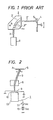
- the present invention relates to an ion implanter for implanting ions of a predetermined sort into a sample such as semiconductor wafer.
- FIG. 1 shows the fundamental setup of a prior-art ion implanter.
- an ion beam 3 emergent from an ion source 1 is separated into ion beams 3', 3", 3"' etc. of individual ion sorts by a static magnetic field B which a magnetic mass separator 2 establishes.
- a semiconductor wafer 5 is mounted on the surface of a sample holder 4.
- the holder is mounted on the surface of a rotating disk.
- the semiconductor wafer 5 is uniformly irradiated with the ion beam 3" consisting only of predetermined ions.
- the mass resolution of the magnetic mass separator 2 is proportional to the beam radius rm in the magnetic sector.
- the radius r m has to be increased. Therefore, the magnetic mass separator 2 and the whole ion implanter becomes large in size.
- the transmissivity of the mass separator 2 for the ion beam is usually several tens %, and the beam loss is inevitable. Accordingly, the effective utilization factor of the ion implanting current compared to the ion beam 3 extracted from the ion source 1 is ordinarily 30% or so.
- GB-A-20 52 146 discloses an ion implantation apparatus which comprises a mass analyzer and a magnetic type beam deflector.
- the beam reflector is disposed between the mass analyzer and the target and is used to laterally deflect the particle beam emanting from the mass analyzer.
- the beam deflector comprises an A.C.-driven electromagnet in order to prevent lateral velocity components of the ions emerging therefrom. While such an ion implantation apparatus is useful to avoid the disadvantages resulting from lateral velocity components and the corresponding variable angle of incidence of the ions, it still has a drawback of low transmissivity.
- an ion implanter is constructed of an ion source, a sample holder for supporting a sample to be implanted with ions, and scanning means for scanning an ion beam extracted from said ion source, the sample being located at a position where it avoids irradiation with neutral particles which propagate rectilinearly from said ion source.
- the scanning means is constructed of a permanent magnet which is disposed between said ion source and the sample, and an A.C. power supply which is connected to said ion source in order to impose small fluctuations in the ion acceleration energy.
- Figure 2 shows the fundamental setup of an ion implanter according to the present invention.
- a semiconductor wafer 5 placed on a sample holder (not shown) is located in the direction in which an ion beam 3 from an ion source 1 propagates rectilinearly.
- a static magnetic field is imposed by using a peranent magnet 8.
- the ion beam 3 is deflected in the static magnetic field generated by the permanent magnet 8, depending upon the voltage of a D.C. power supply (V DC ) 12 for extracting the ion beam 3 from the ion source 1.
- V DC D.C. power supply
- the setup is so arranged that the ion beam 3 impinges upon the center of the semiconductor wafer 5.
- one end part A of the semiconductor wafer 5 has its position shifted sideways so as not to be irradiated with neutral particles which propagate rectilinearly from the ion source 1.
- fast neutral particles emergent from the ion source 1 are prevented from becoming implanted into the semiconductor wafer 5.
- Neutral particle implantation results in dose non-uniformity over the semiconductor wafer 5.
- an A.C. voltage from the A.C. power supply (VAC) 11 is superposed on the D.C. voltage from the D.C. power supply (V oc ) 12, whereby the ion beam 3 is laterally oscillated on the semiconductor wafer 5 as indicated by arrows.
- the semiconductor wafer 5 is mechanically moved perpendicularly to the sheet of the drawing.
- the semiconductor wafer 5 is uniformly irradiated with the ion beam 3. Since the extraction voltage of the ion beam 3 fluctuates due to the application of the A.C. voltage, the extraction characteristics of the ion beam 3 change. In the experiment, however, the A.C. voltage V AC was approximately 1 -2kV, when the D.C. acceleration voltage V oc was 30kV. The voltage fluctuation to this degree scarcely changes the extraction characteristics (beam current and shape).
- numeral 13 designates a plasma chamber, numeral 10 a negative electrode and numeral 9 a ground electrode, and these constitute the ion source 1.
- the ion beam 3 is scanned with the center on the semiconductor wafer 5. In the embodiment shown in Fig. 2, the amplitude of the oscillations can be made small, and the utilization factor of the beam current is improved.
- the mass separator 2 is not included, and the distance between the ion source 1 and the semiconductor wafer 5 is shortened. Therefore, loss of the ion beam 3 becomes extremely low, and the ion beam 3 extracted from the ion source 1 can be effectively utilized as it is.
- ion implanter In the ion implanter according to the present invention, mass separation is not performed.
- an ion source arrangement in which a solid material corresponding to the sort of implant ions is heated and vaporized and then introduced into the ion source 1, and the vapor is used as a working gas for the ion source 1, whereby the purity of the ion beam to be extracted is enhanced.
- the ion source arrangement it is possible to use, for example, a coaxial microwave ion source as disclosed in Japanese Patent Application No. 55-152140.
- ion implantation with a high current ion beam is realized without degrading the uniformity of the ion implantation, and the effect is remarkable in practical use.
Landscapes
- Chemical & Material Sciences (AREA)
- Analytical Chemistry (AREA)
- Physical Vapour Deposition (AREA)
Claims (4)
Applications Claiming Priority (2)
| Application Number | Priority Date | Filing Date | Title |
|---|---|---|---|
| JP7050781U JPS57182864U (de) | 1981-05-18 | 1981-05-18 | |
| JP70507/81 | 1981-05-18 |
Publications (2)
| Publication Number | Publication Date |
|---|---|
| EP0066175A1 EP0066175A1 (de) | 1982-12-08 |
| EP0066175B1 true EP0066175B1 (de) | 1985-09-04 |
Family
ID=13433509
Family Applications (1)
| Application Number | Title | Priority Date | Filing Date |
|---|---|---|---|
| EP82104325A Expired EP0066175B1 (de) | 1981-05-18 | 1982-05-17 | Ionenimplantationsvorrichtung |
Country Status (3)
| Country | Link |
|---|---|
| EP (1) | EP0066175B1 (de) |
| JP (1) | JPS57182864U (de) |
| DE (1) | DE3266001D1 (de) |
Families Citing this family (4)
| Publication number | Priority date | Publication date | Assignee | Title |
|---|---|---|---|---|
| US5389793A (en) * | 1983-08-15 | 1995-02-14 | Applied Materials, Inc. | Apparatus and methods for ion implantation |
| EP0135366B1 (de) * | 1983-08-15 | 1990-11-07 | Applied Materials, Inc. | System und Methode zur Ionenimplantation |
| US4578589A (en) * | 1983-08-15 | 1986-03-25 | Applied Materials, Inc. | Apparatus and methods for ion implantation |
| ATE168819T1 (de) * | 1991-03-25 | 1998-08-15 | Commw Scient Ind Res Org | Makroteilchenfilter in lichtbogenquelle |
Family Cites Families (2)
| Publication number | Priority date | Publication date | Assignee | Title |
|---|---|---|---|---|
| FR2133315A5 (de) * | 1971-04-16 | 1972-11-24 | Thomson Csf | |
| GB2052146B (en) * | 1979-06-04 | 1983-06-22 | Varian Associates | Unitary electromagnet for double deflection scanning of charged particle beam |
-
1981
- 1981-05-18 JP JP7050781U patent/JPS57182864U/ja active Pending
-
1982
- 1982-05-17 DE DE8282104325T patent/DE3266001D1/de not_active Expired
- 1982-05-17 EP EP82104325A patent/EP0066175B1/de not_active Expired
Non-Patent Citations (3)
| Title |
|---|
| IBM TECHNICAL DISCLOSURE BULLETIN, vol.19, no.9, February 1977, New York (US) J.R.WINNARD: " Ion-beam scanning by magnetic means", pages 3411-3412. * |
| JOURNAL OF VACUUM SCIENCE AND TECHNOLOGY, vol.13, no.5, September-October 1976, New York (US) G.RYDING et al.: "Features of high-current implanter and medium-current implanter" pages 1030-1036. * |
| WESCON TECHNICAL PAPERS, vol.15, 1971, Hollywood (US)J.N.CECIL et al.: " Particle accelerators for ion implantation " pages 1-6. * |
Also Published As
| Publication number | Publication date |
|---|---|
| JPS57182864U (de) | 1982-11-19 |
| DE3266001D1 (de) | 1985-10-10 |
| EP0066175A1 (de) | 1982-12-08 |
Similar Documents
| Publication | Publication Date | Title |
|---|---|---|
| US6313475B1 (en) | Acceleration and analysis architecture for ion implanter | |
| US6777696B1 (en) | Deflecting acceleration/deceleration gap | |
| US4661712A (en) | Apparatus for scanning a high current ion beam with a constant angle of incidence | |
| US6060715A (en) | Method and apparatus for ion beam scanning in an ion implanter | |
| US5751002A (en) | Ion implantation apparatus | |
| US5126575A (en) | Method and apparatus for broad beam ion implantation | |
| EP0428319A2 (de) | Verfahren und Gerät zur Erzeugung eines elliptisch verteilten Ionenstrahls | |
| WO2005086204A2 (en) | Modulating ion beam current | |
| KR100479374B1 (ko) | 원추 자기 주사를 사용하는 이온 빔 주입 장치 및 방법 | |
| US5719403A (en) | MeV scanning ions implanter | |
| EP0445964A2 (de) | Vorrichtung und Verfahren zur Ablenkung von Ionenstrahlen | |
| US6897457B1 (en) | Apparatus and method for monitoring and tuning an ion beam in ion implantation apparatus | |
| JPS62108438A (ja) | 空間電荷レンズを使用した高電流質量分光計 | |
| EP0066175B1 (de) | Ionenimplantationsvorrichtung | |
| KR100439936B1 (ko) | 리본빔을발생시키는이온주입장치,상기이온주입장치에사용하기위한플라즈마전극,및가공물을이온빔으로처리하는방법 | |
| KR0143433B1 (ko) | 이온주입기 | |
| JPH01252771A (ja) | イオン注入装置 | |
| JPH01252773A (ja) | イオン注入装置 | |
| JPH06302293A (ja) | マイクロ波イオン源 | |
| JPH02260356A (ja) | イオン注入装置における平行走査系 | |
| JPS60236446A (ja) | イオン打込み装置 | |
| JPH07153415A (ja) | イオン打ち込み方法及びその実施装置 |
Legal Events
| Date | Code | Title | Description |
|---|---|---|---|
| PUAI | Public reference made under article 153(3) epc to a published international application that has entered the european phase |
Free format text: ORIGINAL CODE: 0009012 |
|
| AK | Designated contracting states |
Designated state(s): DE FR GB NL |
|
| 17P | Request for examination filed |
Effective date: 19830131 |
|
| GRAA | (expected) grant |
Free format text: ORIGINAL CODE: 0009210 |
|
| AK | Designated contracting states |
Designated state(s): DE FR GB NL |
|
| REF | Corresponds to: |
Ref document number: 3266001 Country of ref document: DE Date of ref document: 19851010 |
|
| ET | Fr: translation filed | ||
| PLBE | No opposition filed within time limit |
Free format text: ORIGINAL CODE: 0009261 |
|
| STAA | Information on the status of an ep patent application or granted ep patent |
Free format text: STATUS: NO OPPOSITION FILED WITHIN TIME LIMIT |
|
| 26N | No opposition filed | ||
| PGFP | Annual fee paid to national office [announced via postgrant information from national office to epo] |
Ref country code: GB Payment date: 20010426 Year of fee payment: 20 |
|
| PGFP | Annual fee paid to national office [announced via postgrant information from national office to epo] |
Ref country code: NL Payment date: 20010427 Year of fee payment: 20 |
|
| PGFP | Annual fee paid to national office [announced via postgrant information from national office to epo] |
Ref country code: FR Payment date: 20010502 Year of fee payment: 20 |
|
| PGFP | Annual fee paid to national office [announced via postgrant information from national office to epo] |
Ref country code: DE Payment date: 20010629 Year of fee payment: 20 |
|
| REG | Reference to a national code |
Ref country code: GB Ref legal event code: IF02 |
|
| PG25 | Lapsed in a contracting state [announced via postgrant information from national office to epo] |
Ref country code: GB Free format text: LAPSE BECAUSE OF EXPIRATION OF PROTECTION Effective date: 20020516 |
|
| PG25 | Lapsed in a contracting state [announced via postgrant information from national office to epo] |
Ref country code: NL Free format text: LAPSE BECAUSE OF EXPIRATION OF PROTECTION Effective date: 20020517 |
|
| REG | Reference to a national code |
Ref country code: GB Ref legal event code: PE20 Effective date: 20020516 |
|
| NLV7 | Nl: ceased due to reaching the maximum lifetime of a patent |
Effective date: 20020517 |