EP0062471A2 - Thin film solar cell - Google Patents
Thin film solar cell Download PDFInfo
- Publication number
- EP0062471A2 EP0062471A2 EP82301632A EP82301632A EP0062471A2 EP 0062471 A2 EP0062471 A2 EP 0062471A2 EP 82301632 A EP82301632 A EP 82301632A EP 82301632 A EP82301632 A EP 82301632A EP 0062471 A2 EP0062471 A2 EP 0062471A2
- Authority
- EP
- European Patent Office
- Prior art keywords
- thin film
- solar cell
- silicon
- film
- substrate
- Prior art date
- Legal status (The legal status is an assumption and is not a legal conclusion. Google has not performed a legal analysis and makes no representation as to the accuracy of the status listed.)
- Granted
Links
Images

Classifications
-
- H—ELECTRICITY
- H10—SEMICONDUCTOR DEVICES; ELECTRIC SOLID-STATE DEVICES NOT OTHERWISE PROVIDED FOR
- H10F—INORGANIC SEMICONDUCTOR DEVICES SENSITIVE TO INFRARED RADIATION, LIGHT, ELECTROMAGNETIC RADIATION OF SHORTER WAVELENGTH OR CORPUSCULAR RADIATION
- H10F77/00—Constructional details of devices covered by this subclass
- H10F77/10—Semiconductor bodies
- H10F77/16—Material structures, e.g. crystalline structures, film structures or crystal plane orientations
- H10F77/162—Non-monocrystalline materials, e.g. semiconductor particles embedded in insulating materials
- H10F77/164—Polycrystalline semiconductors
- H10F77/1642—Polycrystalline semiconductors including only Group IV materials
-
- H—ELECTRICITY
- H10—SEMICONDUCTOR DEVICES; ELECTRIC SOLID-STATE DEVICES NOT OTHERWISE PROVIDED FOR
- H10F—INORGANIC SEMICONDUCTOR DEVICES SENSITIVE TO INFRARED RADIATION, LIGHT, ELECTROMAGNETIC RADIATION OF SHORTER WAVELENGTH OR CORPUSCULAR RADIATION
- H10F77/00—Constructional details of devices covered by this subclass
- H10F77/10—Semiconductor bodies
- H10F77/16—Material structures, e.g. crystalline structures, film structures or crystal plane orientations
- H10F77/169—Thin semiconductor films on metallic or insulating substrates
- H10F77/1692—Thin semiconductor films on metallic or insulating substrates the films including only Group IV materials
-
- Y—GENERAL TAGGING OF NEW TECHNOLOGICAL DEVELOPMENTS; GENERAL TAGGING OF CROSS-SECTIONAL TECHNOLOGIES SPANNING OVER SEVERAL SECTIONS OF THE IPC; TECHNICAL SUBJECTS COVERED BY FORMER USPC CROSS-REFERENCE ART COLLECTIONS [XRACs] AND DIGESTS
- Y02—TECHNOLOGIES OR APPLICATIONS FOR MITIGATION OR ADAPTATION AGAINST CLIMATE CHANGE
- Y02E—REDUCTION OF GREENHOUSE GAS [GHG] EMISSIONS, RELATED TO ENERGY GENERATION, TRANSMISSION OR DISTRIBUTION
- Y02E10/00—Energy generation through renewable energy sources
- Y02E10/50—Photovoltaic [PV] energy
- Y02E10/546—Polycrystalline silicon PV cells
Definitions
- the present invention relates to a solar cell using a silicon film.
- the single-crystalline solar cell has the highest photoelectric conversion efficiency of the three types of cells, but it must be subjected to a high temperature processing in its fabrication, which results in that the production cost becomes relatively high.
- the amorphous silicon solar cell has an advantage that the production cost becomes relatively low because the cell is fabricated or formed at a low temperature, but it also has a disadvantage that its photoelectric conversion efficiency has been about 1/2 to 1/3 of that of the single-crystalline cell.
- the conversion efficiency of the polycrystalline silicon cell will be between those of the single-crystalline and amorphous silicon cells.
- recombination centers at or around grain boundaries in the polycrystalline silicon work to reduce the conversion efficiency. For this reason, the efficiency will be remarkably reduced as the grain size becomes small, which makes it difficult to form a thin film solar cell of good efficiency with micro-crystalline grains.
- a silicon film of a mixed phase which mainly consists of fibrous crystalline grains and in which the recombination centers in the vicinity of the grain boundaries are terminated by different sorts of elements.
- fibrous crystalline grains take columnar or cone-like shape and long in the direction of growth. However, they are not limited to long grains as will be described later.
- an embodiment of the present invention provides a thin film solar cell which comprises a predetermined substrate, at least a transparent first electrode and a second electrode, a thin film mainly formed of silicon and interposed between said first and second electrodes, and at least one barrier formed in the thin film for separating photo-ionized carriers (electrons and positive holes), wherein said silicon film comprises a mixed phase of polycrystalline phase and amorphous phase, and contains 50% or more of such fibrous crystalline grains by volume ratio that has a bottom diameter not larger than 1 ⁇ m and a height of at least 50 nm, and the grain boundaries thereof are substantially terminated.
- the substrate can concurrently work as one of the electrodes when made of a conductor.
- the barrier may be formed of a grown pn junction, other junctions or contacts which establish a built-in field or potential barrier.
- the general orientation of the longitudinal (growth) directions of fibrous grains forms an angle of 45° to 90° with respect to said barrier plane.
- the crystalline grain boundaries in said silicon film are terminated by at least one selected from the group consisting of hydrogen, oxygen, fluorine, chlorine, iodine, lithium, sodium, potassium, cesium and rubidium.
- Terminated amorphous silicon may be characterized in that its optical absorption coefficient around the peak wavelength of solar radiation is greater than that of single-crystalline silicon by one order of magnitude or more. Therefore, a thin amorphous silicon of about 1 ⁇ m in thickness is sufficient to effectively absorb solar light energy around the peak wavelength. In other words, the amount of amorphous silicon necessary for a solar cell can be considerably reduced compared to the fact that a single-crystalline silicon solar cell must have a thickness of the order of about 100 ⁇ m or more from the mechanical reasons. Amorphous silicon solar cell which is formed on an appropriate substrate is considered to be effective for saving resources.
- the inventors have found that a large optical absorption coefficient comparable to that of the amorphous film can also be obtained by the polycrystalline film provided that the grain size in the polycrystalline silicon film must be made sufficiently small. This may be considered to arise from the fact that the grain boundaries and/or the vicinity thereof in a polycrystalline film has the similar bonding state to that of the amorphous material (loss of crystal symmetry) thereby exhibiting a large optical absorption coefficient.Such a film may be considered to be in a mixed phase of crystalline phase and amorphous phase, which state is referred to as a mixed phase in this specification.
- the optical absorption coefficient of the mixed phase material depends on the volume ratio of the crystalline phase portion and the amorphous phase portion, and further on the grain size distribution. Generally, the smaller the size of micro-crystalline grain is, the larger the absorption coefficient is. Also, as the grain size becomes larger the absorption coefficient tends to be close to that of the monocrystalline material.
- the recombination centers are mainly associated with dangling bonds. Therefore, if the dangling bonds are terminated by at least one selected from the group consisting of atoms and atom groups including such elements as hydrogen, oxygen, fluorine, chlorine, iodine, lithium, sodium, potassium, cesium and rubidium, then the recombination centers will be remarkably decreased in number and thus the polycrystalline silicon film will exhibit a high photo-conductive property. Most of the added elements are introduced not into the interior of the crystal grains but in the vicinity of the grain boundaries. Said group of elements are monovalent elements such as halogen elements or monovalent metallic elements.
- the polycrystalline silicon film thus terminated can be regarded as a mixed phase film having crystalline phase and terminated amorphous phase disposed in the vicinity of the grain boundaries.
- the diffusion length of positive holes generated by incident rays is reported to be about 50 nm which is very short compared with several tens microns in the crystalline silicon, while the diffusion length of electrons is of-the order of 500 to 1000 nm. For this reason, the efficiency of the electrons and positive holes generated by light in the terminated amorphous silicon diffusing to the junction portion of the solar cell and contributing-.to electric-generation is smaller than that in the single-crystalline silicon which has larger diffusion lengths. Therefore, the photo-electric conversion efficiency in the amorphous silicon is still low.
- the film structure of a solar battery is so arranged that electrons and positive holes are generated in a terminated amorphous phase portion and are caused to diffuse or flow under the influence of a built-in electrical field into crystalline phase portions and then to move through the crystalline phase portion in the vertical direction to the junction portion of the solar battery, the film will have a larger optical absorption coefficient than that of a single-crystalline film and also have a longer mean diffusion length of electrons and positive holes than the diffusion length of the terminated amorphous film.
- a polycrystalline silicon film grown on a glass or stainless steel substrate may comprise crystalline grains of column-like and/or cone-like structure, that is so-called fibrous structure standing on the substrate under certain conditions. Accordingly, if such a film structure could be made that electrons and positive holes generated in a terminated amorphous phase portion will diffuse or flow under the influence of a built-in electrical field into crystalline phase portions to move through the crystalline phase in the vertical direction to the junction plane of the solar cell; then the effective diffusion length can become about the same as that of electrons and holes in crystalline phase, whereby the photo-electric conversion efficiency and thus carrier collection efficiency will increase.
- a substrate 1 is made of glass, ceramic, metal (for example, stainless steel or nickel) or thermostable high-polymer resin (for example, polyimide resin).
- a lower metallic electrode 2 may be deposited on the substrate. If the substrate is made of a conductive material, then the substrate can be also used as an electrode.
- a fibrous (column-like and/or cone-like) polycrystalline silicon film 3 is formed on the electrode 2.
- the polycrystalline silicon film 3 can be formed by the thermal decomposition CVD (chemical vapour deposition) process, the glow discharge CVD process, the sputtering process, the ion plating process, the high frequency sputtering process, the ultra-high vacuum deposition process, or other various processes.
- CVD chemical vapour deposition
- the sputtering process the ion plating process
- the high frequency sputtering process the ultra-high vacuum deposition process
- the ultra-high vacuum deposition process or other various processes.
- the deposition rate is too fast or the temperature of the substrate is too low or the atmosphere in formation of the polycrystalline film contains too many hydrogen or oxygen atoms, then it becomes difficult to grow a film in the form of large fibrous crystalline grains and growth of amorphous phase or smaller micro-crystalline grains will result.
- the condition of forming the film must be suitably controlled.
- the conductivity of the film can be controlled by properly adding or doping small quantity of P-type or N-type impurity into the atmospheric gas or into the raw silicon material.
- an ohmic contact is formed between the lower electrode 2 and the polycrystalline silicon film 3, and PN-junctions are formed in the polycrystalline silicon film 3.
- the PN-junction forming technique based on thermal diffusion is not preferable in the case of polycrystalline film devices, although it is usually used preferably in the case of formation of single-crystalline silicon devices.
- N + or P + type layer adjacent to the interface with the lower electrode 2 will enhance the formation of an ohmic contact with respect to the electrode.
- a highly doped layer is formed adjacent to an electrode layer, a polycrystalline film which has large grain sizes can be formed. at a low temperature. This is convenient for the formation of a structure suited to the present invention.
- the thickness of the N + or P type layer is preferably between 5 nm and 1 ⁇ m.
- the film is terminated to quench and diminish dangling bonds in the vicinity of the grain boundaries.
- the termination is carried out by heat-treating the polycrystalline film 3 in a plasma atmosphere containing at least one element selected from the group consisting of hydrogen, oxygen, fluorine, chlorine, iodine, lithium, sodium, potassium, cesium and rubidium, etc.
- the quantity of element doped in the polycrystalline film 3 is between about 10 ppm by atomic ratio and about 5 atomic-%. When the doped quantity is in the above range, the photoelectric conversion efficiency of the resulting polycrystalline film can become high enough to allow practical applications of the film, although it also depends on the grain size to some extent.
- terminated amorphous silicon Since terminated amorphous silicon has usually a wider forbidden band than crystalline silicon, the following two phenomena or actions will take place in the vicinity of the interface between the terminated amorphous phase portion and crystalline phase portion. Firstly, since a thin terminated amorphous layer of wider band gap covers the surface of each crystalline grain at least in the vicinity of the surface of the solar cell through which light rays pass into the film 3, recombinations at the light receiving surface is suppressed, i.e., an window effect takes place, whereby the photoelectric conversion efficiency from incident ray energy to electrical energy can be raised.
- the interface or grain boundary between the crystalline grains and the terminated amorphous silicon layers 'could be as illustrated in Fig. 2.
- electron-positive hole pairs generated in the terminated amorphous layer having a wider forbidden band are moved into the grains under the influence of a built-in electrical field established around the interface between the amorphous layer and the grain and are collected.
- a field is preferably generated in such a manner that most of the minority carriers generated in the amorphous layer will be moved into the adjacent grains.
- the electron-positive hole pairs generated in the amorphous phase are advantageously separated spatially, whereby the possibility of recombination can be reduced.
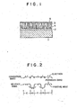
- reference character "a” refers to an amorphous region and reference character “c" refers to a crystalline region.
- the height of fibrous (column-like and/or cone-like) crystalline grains is high so that the fibrous grains are continuous in the main part of the film thickness, in contrast to the diameter of the bottom surface of each grain, and that the direction of growth of each fibrous grain is substantially vertical to the junction or barrier plane of the solar cell.
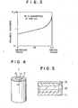
- Fig. 3 shows a graph showing the relationship between the film thickness required for absorbing 96% of the light of wavelength about 550 nm which is the peak wavelength in solar radiation energy, and the volume ratio of crystalline grain contained in the film including terminated amorphous phase and crystalline phase. It will be readily seen from Fig. 3 that if the terminated amorphous silicon layer has a thickness of at least 0.5 ⁇ m, the film can sufficiently absorb the above-mentioned light. On the other hand, if the film contains 50% of crystalline phase by volume percentage, the necessary film thickness will be increased about twice.
- the film contains some several tens volume percent (i.e. around 50% by volume) of crystalline phase for enhancing the transport of carriers. Also, the effect of the mixture of amorphous phase becomes clear when about 0.1% by volume of amorphous phase is present and becomes significant when about 1% by volume of amorphous phase is present.
- each fibrous crystal grain (whose radius is r l ) 6 is surrounded, in this example, by an amorphous state layer 7 (whose outer radius is r 2 ) of 50 nm in thickness corresponding to the diffusion length of carriers in the amorphous phase layers.
- the film contains about 80% of crystalline phase by volume percentage. It will be understood that the practical film structure is not so simple as described above and hence the volume ratio of the crystal grain will be altered according to the various conditions.
- the above consideration is very important in practical formation of the film structure according to the present invention. That is, it is common practice to form the film by first forming fibrous (column-like or cone-like) crystalline phase film by a proper process and subsequently by terminating dangling bonds in the vicinity of interfaces or grain boundaries with the use of the above-said plasma process.
- the depth into crystalline grains effected by the plasma process is independent substantially of the grain size. Therefore, in the case where the volume ratio of crystalline phase to terminated amorphous phase should be controlled in a plasma processing time, the simplest way is to control the size of crystalline grains to be prepared.
- the height of fibrous crystalline grains is preferably as high as possible in a given film thickness as has been explained above, and thus "grain size" to be controlled will refer to the diameter of the bottom surface of a fibrous (column-like or cone-like) crystalline grain.
- the grain size of the polycrystalline film must be 1 ⁇ m at most in order for the film to be terminated by the plasma process and to exhibit mixed phase features including the high optical absorption coefficient.
- the film has a larger grain size than 1 ⁇ m, i.e., larger than the most of the wavelengths of the incident ray, then the film can not be found to have a clear difference in optical absorption coefficient from that of a single-crystalline film.
- it is desirable that the height of crystalline grains is longer than the diffusion length of positive holes in amorphous phase layers, that is, 50 nm.
- the crystalline grains should contain at least 50% of such fibrous (column-like and/or cone-like) grains by volume percentage, that have a diameter of the bottom surface at most equal to about 1 ⁇ m (usually, the 0 diameters being larger than 30 or 50 A), and a height at least equal to about 50 nm (usually, heights being below 100 pm).
- the general orientation of the grain heights is not substantially vertical to the junction or barrier face of the solar cell, the effect of the present invention will be diluted or weakened. Therefore, it is preferable that the general orientation of the direction of growth of grains forms an angle of 45° to 90° with respect to the junction or barrier face.
- h k denotes a height vector of a fibrous (column-like or cone-like) crystalline grain in the film
- N denotes the total number of crystalline grains under interest.
- the thickness of silicon film for the solar cell is in the range of about 5000 A to about 5 ⁇ m and thus it is about the same as that of an ordinary film.
- FIG. 5 a cross-sectional view of the basic structure of a thin film solar cell in accordance with an embodiment of the present invention.
- a stainless steel substrate 11 mirror-polished at its surface is placed in a vacuum chamber and the chamber is put under a vacuum of 1 x 10 -4 Torr.
- the substrate is heated to 500°C, and is exposed to an Ar gas which contains 10% of SiH 4 and which is flowing at a velocity of 100 cc/min. Then, the gas is discharged under the following conditions; a pressure of 1 Torr, and input power having a high frequency of 13.56 MHz and a power of 100 W. That is, a polycrystalline silicon film 12 of 2 ⁇ m in thickness is deposited on the substrate 11 by the so-called plasma CVD process. The deposition rate is about 2 A/sec.
- crystalline grains contained in the formed silicon film have a bottom surface diameter of 0.2 ⁇ m and an average height of 1 ⁇ m.
- the film is exposed in plasma environment formed in a hydrogen atmosphere of 5 x 10 Torr for a period of one hour at a substrate temperature of 300°C (in which case, an input power has a high frequency of 13.56 MHz and a power or 50 W), for the purpose of termination processing of dangling bonds.
- the amount of hydrogen atoms contained in the film is about 0.1 atom. percent.
- indium-tin oxide is sputtered on the polycrystalline silicon film 12 at a substrate temperature of 150°C to form a transparent electrode 13 of 100 nm in thickness, whereby a solar cell has been completed.
- hydrogen element has been used in this embodiment as an element introduced into grain boundaries of the polycrystalline silicon film 12, oxygen or any halogen element such as fluorine, chlorine, bromine, iodine or combinations thereof, or alternatively any monovalent metallic element such as lithium, sodium, potassium, cesium, rubidium or combinations thereof may be used.
- halogen element such as fluorine, chlorine, bromine, iodine or combinations thereof
- monovalent metallic element such as lithium, sodium, potassium, cesium, rubidium or combinations thereof
- Fig. 6 shows a graph showing an exemplary relationship between the hydrogen content in the silicon film obtained in Embodiment 1 and the photo- electric conversion efficiency (n) of the solar cell based on the film.
- a conversion efficiency available for practical application can be obtained in the range of above 10 ppm, but it is practically impossible to operate or use the film in the range of above 5 atom percent because of its difficulty of introducing hydrogen atoms into the silicon film upon formation of the film.
- Table 1 illustrates conversion efficiencies for different elements introduced into silicon films.
- the basic forming procedure of the films are same as in the above embodiment.
- “None” means a case where no termination processing of dangling bonds is performed in the above-mentioned production steps for the purpose of comparison.
- the alumina substrate 1 with the molybdenum electrode 2 deposited at its surface is placed in a vacuum chamber, and the polycrystalline silicon film 3 of 3 ⁇ m in thickness is formed on the molybdenum electrode 2 at a substrate temperature of 550°C by the ion plating process. Crystalline grains contained in the resulting silicon film 3 have a bottom surface diameter of 0.3 ⁇ m and an average height of about 1 ⁇ m.
- silicon doped with Ga or Sb or a pure silicon is used as raw material so that a P + layer of 15 nm in thickness, an I layer of 2800 nm and an N + layer of 5 nm are formed sequentially from the substrate side.
- the substrate is kept at a temperature of 550°C and an HF gas of 5 x 10 -3 Torr is introduced into the vacuum chamber. Then, the prepared substrate is exposed in plasma formed in the HF gas by an input rf power of 50 W and 13.56 MHz for 30 minutes. This plasma processing will cause the grain boundaries in the polycrystalline silicon to be terminated. At this stage, the amount of hydrogen atoms contained in the silicon film is about 0.2 atom percent. Subsequently, a mixture of SnCl 4 gas and H 2 0 gas added to an N 2 gas of 1 atmosphere is guided on the silicon film which is kept at a temperature of 550°C so as to form the transparent electrode 5 on the film 3 through its thermal decomposition. At this point, a solar cell has been completed. The conversion efficiency of the obtained cell was in the range from about 5.5 to about 6.0%.
- a hard glass substrate having a tantalum film sputtered on its surface as a translucent electrode is placed in a vacuum chamber.
- the substrate is kept at a temperature of 600°C, and in the environment of an A r gas of 3 x 10 -3 Torr and a polycrystalline silicon film of 1 ⁇ m in thickness is formed on the surface of the substrate by means of sputtering with the use of a silicon target.
- Crystalline grains contained in the resultant film have a bottom surface diameter of 0.2 ⁇ m and an average height of about 0.8 ⁇ m.
- the target is replaced sequentially with an In-doped silicon, a pure silicon and an As-doped silicon so as to form a P layer of 50 nm in thickness, an I layer of 900 nm and an N + layer of 50 nm.
- a NaCl gas is introduced into the vacuum chamber.
- the prepared substrate is exposed in the plasma formed in Ar gas having NaCl at a substrate temperature of 600°C in the chamber.
- the amount of Na atoms contained in the resulting silicon film is about 0.1 atom percent.
- an aluminium electrode is deposited to obtain a solar cell. In this case, light is passed from the side of the glass substrate. The conversion efficiency of the solar cell was about 5%.
- An alumina substrate with a molybdenum electrode sputtered at its surface is placed in a vacuum chamber.
- the substrate is kept at 700°C and a mixture gas of SiF 4 , SiH 4 and H 2 is introduced into the chamber under a pressure of 1 Torr.
- a 4 ⁇ m layer of polycrystalline silicon is formed on the substrate under a glow discharge by an RF power source of 200 W.
- a PH 3 gas having a partial pressure of 1.3 x 10 -3 Pa is introduced into the chamber at the beginning stage of the desposition whereas a B 2 H 6 gas having a partial pressure of 1.3 x 10 -3 Pa is introduced thereinto at the ending stage thereof, so that an N + layer of 100 nm in thickness, an I layer of 3800 nm and a P layer of 100 nm are formed in sequence from the substrate side.
- Crystalline grains contained in the resulting silicon film have a bottom surface diameter of 0.4 ⁇ m and an average height of 1.2 ⁇ m.
- the silicon film so obtained is already F terminated without use of the plasma process and contains fibrous crystalline grains which have a high photo-conductivity.
- the amount of F atoms contained in the resultant film was about 0.8 atom percent.
- indium-tin oxide is sputtered at a substrate temperature of 350°C to form a transparent electrode.
- the obtained solar cell was about 6.5% in conversion efficiency.
- the thin film solar cell according to the present invention has a composition similar to crystalline phase and exhibits a high photoelectric conversion efficiency, whereby the solar cell can be manufactured inexpensively and find a wide range of industrial applications.
Landscapes
- Photovoltaic Devices (AREA)
Abstract
Description
- The present invention relates to a solar cell using a silicon film.
- There have been, so far, proposed three types of silicon solar batteries or cells; those using a single crystalline silicon, those using a polycrystalline silicon, and those using an amorphous silicon terminated with hydrogen, fluorine, etc.; some of which have been already put into practice. An example of the amorphous silicon solar cell is disclosed in Appl. Phys.
- Lett. 28 (1976), page 671, by D.E. Carlson and C.R. Wronski.
- In general, the single-crystalline solar cell has the highest photoelectric conversion efficiency of the three types of cells, but it must be subjected to a high temperature processing in its fabrication, which results in that the production cost becomes relatively high. On the other hand, the amorphous silicon solar cell has an advantage that the production cost becomes relatively low because the cell is fabricated or formed at a low temperature, but it also has a disadvantage that its photoelectric conversion efficiency has been about 1/2 to 1/3 of that of the single-crystalline cell. The conversion efficiency of the polycrystalline silicon cell will be between those of the single-crystalline and amorphous silicon cells. However, recombination centers at or around grain boundaries in the polycrystalline silicon work to reduce the conversion efficiency. For this reason, the efficiency will be remarkably reduced as the grain size becomes small, which makes it difficult to form a thin film solar cell of good efficiency with micro-crystalline grains.
- Accordingly, it is an object of the present invention to provide a thin film solar cell which eliminates the above defects, has a high conversion efficiency comparable to the single-crystalline solar cell, and can be manufactured at a low production cost.
- According to an aspect of the present invention, there is provided a silicon film of a mixed phase which mainly consists of fibrous crystalline grains and in which the recombination centers in the vicinity of the grain boundaries are terminated by different sorts of elements. Typically, "fibrous" crystalline grains take columnar or cone-like shape and long in the direction of growth. However, they are not limited to long grains as will be described later.
- More specifically, an embodiment of the present invention provides a thin film solar cell which comprises a predetermined substrate, at least a transparent first electrode and a second electrode, a thin film mainly formed of silicon and interposed between said first and second electrodes, and at least one barrier formed in the thin film for separating photo-ionized carriers (electrons and positive holes), wherein said silicon film comprises a mixed phase of polycrystalline phase and amorphous phase, and contains 50% or more of such fibrous crystalline grains by volume ratio that has a bottom diameter not larger than 1 µm and a height of at least 50 nm, and the grain boundaries thereof are substantially terminated. The substrate can concurrently work as one of the electrodes when made of a conductor. The barrier may be formed of a grown pn junction, other junctions or contacts which establish a built-in field or potential barrier.
- It is preferable that the general orientation of the longitudinal (growth) directions of fibrous grains forms an angle of 45° to 90° with respect to said barrier plane. The crystalline grain boundaries in said silicon film are terminated by at least one selected from the group consisting of hydrogen, oxygen, fluorine, chlorine, iodine, lithium, sodium, potassium, cesium and rubidium.
- The above and other objects, features and advantages of the present invention will be apparent from the following detailed description taken in conjunction with the accompanying drawings, in which:
- Fig. 1 is a schematic cross-sectional view, in part, of a silicon-based film solar cell in accordance with an embodiment of the present invention;
- Fig. 2 is an exemplary diagram for explanation of the relationship between the band structures and carriers (electrons and holes) produced or excited by light in the case that the silicon film consists of a mixed phase of crystalline phase and amorphous phase;
- Fig. 3 is a graph showing the relationship between the mixture ratio of the mixed phase and the film thickness necessary for light absorption;
- Fig. 4 is a model diagram of a fibrous crystalline grain which is covered with a terminated amorphous phase;
- Fig. 5 is a major cross-sectional view of a thin film solar cell; and
- Fig. 6 is a graph showing the relationship between the hydrogen content in the silicon film and the photo-electric conversion efficiency.
- Terminated amorphous silicon may be characterized in that its optical absorption coefficient around the peak wavelength of solar radiation is greater than that of single-crystalline silicon by one order of magnitude or more. Therefore, a thin amorphous silicon of about 1 µm in thickness is sufficient to effectively absorb solar light energy around the peak wavelength. In other words, the amount of amorphous silicon necessary for a solar cell can be considerably reduced compared to the fact that a single-crystalline silicon solar cell must have a thickness of the order of about 100 µm or more from the mechanical reasons. Amorphous silicon solar cell which is formed on an appropriate substrate is considered to be effective for saving resources.
- The inventors have found that a large optical absorption coefficient comparable to that of the amorphous film can also be obtained by the polycrystalline film provided that the grain size in the polycrystalline silicon film must be made sufficiently small. This may be considered to arise from the fact that the grain boundaries and/or the vicinity thereof in a polycrystalline film has the similar bonding state to that of the amorphous material (loss of crystal symmetry) thereby exhibiting a large optical absorption coefficient.Such a film may be considered to be in a mixed phase of crystalline phase and amorphous phase, which state is referred to as a mixed phase in this specification. The optical absorption coefficient of the mixed phase material depends on the volume ratio of the crystalline phase portion and the amorphous phase portion, and further on the grain size distribution. Generally, the smaller the size of micro-crystalline grain is, the larger the absorption coefficient is. Also, as the grain size becomes larger the absorption coefficient tends to be close to that of the monocrystalline material.
- Since many recombination centers usually exist in the grain boundaries, the photo-excited electrons and positive holes have short lifetimes, and thus such a polycrystalline silicon will exhibit only a small photo conductivity. These recombination centers are mainly associated with dangling bonds. Therefore, if the dangling bonds are terminated by at least one selected from the group consisting of atoms and atom groups including such elements as hydrogen, oxygen, fluorine, chlorine, iodine, lithium, sodium, potassium, cesium and rubidium, then the recombination centers will be remarkably decreased in number and thus the polycrystalline silicon film will exhibit a high photo-conductive property. Most of the added elements are introduced not into the interior of the crystal grains but in the vicinity of the grain boundaries. Said group of elements are monovalent elements such as halogen elements or monovalent metallic elements. The polycrystalline silicon film thus terminated can be regarded as a mixed phase film having crystalline phase and terminated amorphous phase disposed in the vicinity of the grain boundaries.
- In the terminated amorphous silicon, the diffusion length of positive holes generated by incident rays is reported to be about 50 nm which is very short compared with several tens microns in the crystalline silicon, while the diffusion length of electrons is of-the order of 500 to 1000 nm. For this reason, the efficiency of the electrons and positive holes generated by light in the terminated amorphous silicon diffusing to the junction portion of the solar cell and contributing-.to electric-generation is smaller than that in the single-crystalline silicon which has larger diffusion lengths. Therefore, the photo-electric conversion efficiency in the amorphous silicon is still low.
- If the film structure of a solar battery is so arranged that electrons and positive holes are generated in a terminated amorphous phase portion and are caused to diffuse or flow under the influence of a built-in electrical field into crystalline phase portions and then to move through the crystalline phase portion in the vertical direction to the junction portion of the solar battery, the film will have a larger optical absorption coefficient than that of a single-crystalline film and also have a longer mean diffusion length of electrons and positive holes than the diffusion length of the terminated amorphous film.
- A polycrystalline silicon film grown on a glass or stainless steel substrate may comprise crystalline grains of column-like and/or cone-like structure, that is so-called fibrous structure standing on the substrate under certain conditions. Accordingly, if such a film structure could be made that electrons and positive holes generated in a terminated amorphous phase portion will diffuse or flow under the influence of a built-in electrical field into crystalline phase portions to move through the crystalline phase in the vertical direction to the junction plane of the solar cell; then the effective diffusion length can become about the same as that of electrons and holes in crystalline phase, whereby the photo-electric conversion efficiency and thus carrier collection efficiency will increase.
- There is shown in Fig. 1, in cross section, such a film structure of a solar cell as described above according to an embodiment of the present invention. A substrate 1 is made of glass, ceramic, metal (for example, stainless steel or nickel) or thermostable high-polymer resin (for example, polyimide resin). When the substrate is made of an insulating material, a lower
metallic electrode 2 may be deposited on the substrate. If the substrate is made of a conductive material, then the substrate can be also used as an electrode. Above the substrate, a fibrous (column-like and/or cone-like)polycrystalline silicon film 3 is formed on theelectrode 2. Thepolycrystalline silicon film 3 can be formed by the thermal decomposition CVD (chemical vapour deposition) process, the glow discharge CVD process, the sputtering process, the ion plating process, the high frequency sputtering process, the ultra-high vacuum deposition process, or other various processes. However, if the deposition rate is too fast or the temperature of the substrate is too low or the atmosphere in formation of the polycrystalline film contains too many hydrogen or oxygen atoms, then it becomes difficult to grow a film in the form of large fibrous crystalline grains and growth of amorphous phase or smaller micro-crystalline grains will result. Since a polycrystalline silicon film formed with fibrous crystalline grains is necessary for the achievement of the present invention, the condition of forming the film must be suitably controlled. More specifically, it is necessary to adjust the substrate temperature, the pressure of atmospheric gas, the gas flow rate, the input power, the deposition rate, and so on. On formation of a polycrystalline film, the conductivity of the film can be controlled by properly adding or doping small quantity of P-type or N-type impurity into the atmospheric gas or into the raw silicon material. Using these techniques an ohmic contact is formed between thelower electrode 2 and thepolycrystalline silicon film 3, and PN-junctions are formed in thepolycrystalline silicon film 3. This is referred to as the grown junction technique. The PN-junction forming technique based on thermal diffusion is not preferable in the case of polycrystalline film devices, although it is usually used preferably in the case of formation of single-crystalline silicon devices. This is because the diffusion rate of impurities in grain boundaries is faster than that of impurities in the interior of the crystal grains and thus it is almost impossible to form a uniform junction plane. For this reason, it is desirable to employ not the thermal diffusion technique but the ion implariation or the grown junction technique, in formation of junctions in a thin film solar cell. In this connection, forming a low resistivity N+ or P + type layer adjacent to the interface with thelower electrode 2 will enhance the formation of an ohmic contact with respect to the electrode. When a highly doped layer is formed adjacent to an electrode layer, a polycrystalline film which has large grain sizes can be formed. at a low temperature. This is convenient for the formation of a structure suited to the present invention. The thickness of the N+ or P type layer is preferably between 5 nm and 1 µm. - After having formed the
polycrystalline film 3, the film is terminated to quench and diminish dangling bonds in the vicinity of the grain boundaries. The termination is carried out by heat-treating thepolycrystalline film 3 in a plasma atmosphere containing at least one element selected from the group consisting of hydrogen, oxygen, fluorine, chlorine, iodine, lithium, sodium, potassium, cesium and rubidium, etc. The quantity of element doped in thepolycrystalline film 3 is between about 10 ppm by atomic ratio and about 5 atomic-%. When the doped quantity is in the above range, the photoelectric conversion efficiency of the resulting polycrystalline film can become high enough to allow practical applications of the film, although it also depends on the grain size to some extent. - The heat treatment in a plasma atmosphere is usually effected under the following conditions:
- The atmospheric gas pressure is in the range of 10-3 Pa to 10 Pa, the substrate temperature is in the range of 350°C to 700°C, the high frequency input is in the range of 0.03 W/cm2 to 10 W/cm2 and the frequency of the input is usually 13.56 MHz although it is not limited thereto. Under this treatment, the vicinity of grain boundaries in the
polycrystalline film 3 is terminated. Finally, a proper material such as indium-tin oxide is coated on thefilm 3 to form atransparent electrode 5, for example, by the known sputtering process. - Since terminated amorphous silicon has usually a wider forbidden band than crystalline silicon, the following two phenomena or actions will take place in the vicinity of the interface between the terminated amorphous phase portion and crystalline phase portion. Firstly, since a thin terminated amorphous layer of wider band gap covers the surface of each crystalline grain at least in the vicinity of the surface of the solar cell through which light rays pass into the
film 3, recombinations at the light receiving surface is suppressed, i.e., an window effect takes place, whereby the photoelectric conversion efficiency from incident ray energy to electrical energy can be raised. The interface or grain boundary between the crystalline grains and the terminated amorphous silicon layers 'could be as illustrated in Fig. 2. That is, secondly, electron-positive hole pairs generated in the terminated amorphous layer having a wider forbidden band are moved into the grains under the influence of a built-in electrical field established around the interface between the amorphous layer and the grain and are collected. In this case, a field is preferably generated in such a manner that most of the minority carriers generated in the amorphous layer will be moved into the adjacent grains. Further, in the case of the structure as shown in Fig. 2, the electron-positive hole pairs generated in the amorphous phase are advantageously separated spatially, whereby the possibility of recombination can be reduced. In Fig. 2, reference character "a" refers to an amorphous region and reference character "c" refers to a crystalline region. As a result, most of the minority carriers excited by light are caused to diffuse through crystalline grains so that a high collection efficiency can be obtained when compared with the case where the carriers are diffused through amorphous silicon region having a short diffusion length. As will be clear from the above explanation, it is preferable that electrons and positive holes once moved into crystal grains are diffused to the junction or barrier portion of the solar cell without returning to the amorphous region. Accordingly, it is desirable that the height of fibrous (column-like and/or cone-like) crystalline grains is high so that the fibrous grains are continuous in the main part of the film thickness, in contrast to the diameter of the bottom surface of each grain, and that the direction of growth of each fibrous grain is substantially vertical to the junction or barrier plane of the solar cell. - Although the gist of the invention has been explained in the foregoing, description will next be made quantitatively.
- Fig. 3 shows a graph showing the relationship between the film thickness required for absorbing 96% of the light of wavelength about 550 nm which is the peak wavelength in solar radiation energy, and the volume ratio of crystalline grain contained in the film including terminated amorphous phase and crystalline phase. It will be readily seen from Fig. 3 that if the terminated amorphous silicon layer has a thickness of at least 0.5 µm, the film can sufficiently absorb the above-mentioned light. On the other hand, if the film contains 50% of crystalline phase by volume percentage, the necessary film thickness will be increased about twice. Therefore, when it is taken into consideration that the diffusion length of electrons and positive holes in the amorphous phase is remarkably short, it is preferable that the film contains some several tens volume percent (i.e. around 50% by volume) of crystalline phase for enhancing the transport of carriers. Also, the effect of the mixture of amorphous phase becomes clear when about 0.1% by volume of amorphous phase is present and becomes significant when about 1% by volume of amorphous phase is present.
- Next, explanation will be made in conjunction with such a model of fibrous crystalline grain as shown in Fig. 4.
- Assuming a mixed phase film of amorphous phase layers and fibrous cyrstal grains, and that each fibrous crystal grain (whose radius is rl) 6 is surrounded, in this example, by an amorphous state layer 7 (whose outer radius is r2) of 50 nm in thickness corresponding to the diffusion length of carriers in the amorphous phase layers.


- The above consideration is very important in practical formation of the film structure according to the present invention. That is, it is common practice to form the film by first forming fibrous (column-like or cone-like) crystalline phase film by a proper process and subsequently by terminating dangling bonds in the vicinity of interfaces or grain boundaries with the use of the above-said plasma process. In this case, the depth into crystalline grains effected by the plasma process is independent substantially of the grain size. Therefore, in the case where the volume ratio of crystalline phase to terminated amorphous phase should be controlled in a plasma processing time, the simplest way is to control the size of crystalline grains to be prepared. The height of fibrous crystalline grains is preferably as high as possible in a given film thickness as has been explained above, and thus "grain size" to be controlled will refer to the diameter of the bottom surface of a fibrous (column-like or cone-like) crystalline grain.
- According to experimental results by the inventors, the grain size of the polycrystalline film must be 1 µm at most in order for the film to be terminated by the plasma process and to exhibit mixed phase features including the high optical absorption coefficient. In other words, if the film has a larger grain size than 1 µm, i.e., larger than the most of the wavelengths of the incident ray, then the film can not be found to have a clear difference in optical absorption coefficient from that of a single-crystalline film. According to another aspect of the present invention, it is desirable that the height of crystalline grains is longer than the diffusion length of positive holes in amorphous phase layers, that is, 50 nm. This will be apparent from the fact that in a grain of less than 50 nm in height, carriers cannot travel more than 50 nm without crossing a crystal boundary. Consequently, with the solar cell according to the present invention, the crystalline grains should contain at least 50% of such fibrous (column-like and/or cone-like) grains by volume percentage, that have a diameter of the bottom surface at most equal to about 1 µm (usually, the 0 diameters being larger than 30 or 50 A), and a height at least equal to about 50 nm (usually, heights being below 100 pm). Further, if the general orientation of the grain heights is not substantially vertical to the junction or barrier face of the solar cell, the effect of the present invention will be diluted or weakened. Therefore, it is preferable that the general orientation of the direction of growth of grains forms an angle of 45° to 90° with respect to the junction or barrier face.
- The general orientation of the direction of growth of grain (grain heights) is expressed by the following equation.

- The present invention will be explained with reference to preferred embodiments.
- There is shown in Fig. 5 a cross-sectional view of the basic structure of a thin film solar cell in accordance with an embodiment of the present invention.
- A stainless steel substrate 11 mirror-polished at its surface is placed in a vacuum chamber and the chamber is put under a vacuum of 1 x 10 -4 Torr. The substrate is heated to 500°C, and is exposed to an Ar gas which contains 10% of SiH4 and which is flowing at a velocity of 100 cc/min. Then, the gas is discharged under the following conditions; a pressure of 1 Torr, and input power having a high frequency of 13.56 MHz and a power of 100 W. That is, a
polycrystalline silicon film 12 of 2 µm in thickness is deposited on the substrate 11 by the so-called plasma CVD process. The deposition rate is about 2 A/sec. During formation of the film, 50 ppm of PH3 or 100 ppm of B2H6 is mixed into the raw material gas so that an N+ type layer of 100 nm in thickness, an I type layer of 1.8 µm and a P type layer of 100 nm are formed sequentially from the substrate side. Under these conditions, crystalline grains contained in the formed silicon film have a bottom surface diameter of 0.2 µm and an average height of 1 µm. After the film has been formed, the film is exposed in plasma environment formed in a hydrogen atmosphere of 5 x 10 Torr for a period of one hour at a substrate temperature of 300°C (in which case, an input power has a high frequency of 13.56 MHz and a power or 50 W), for the purpose of termination processing of dangling bonds. At this stage, the amount of hydrogen atoms contained in the film is about 0.1 atom. percent. Thereafter, indium-tin oxide is sputtered on thepolycrystalline silicon film 12 at a substrate temperature of 150°C to form atransparent electrode 13 of 100 nm in thickness, whereby a solar cell has been completed. - Although hydrogen element has been used in this embodiment as an element introduced into grain boundaries of the
polycrystalline silicon film 12, oxygen or any halogen element such as fluorine, chlorine, bromine, iodine or combinations thereof, or alternatively any monovalent metallic element such as lithium, sodium, potassium, cesium, rubidium or combinations thereof may be used. - Fig. 6 shows a graph showing an exemplary relationship between the hydrogen content in the silicon film obtained in Embodiment 1 and the photo- electric conversion efficiency (n) of the solar cell based on the film. As will be seen from the figure, a conversion efficiency available for practical application can be obtained in the range of above 10 ppm, but it is practically impossible to operate or use the film in the range of above 5 atom percent because of its difficulty of introducing hydrogen atoms into the silicon film upon formation of the film.
- Table 1 below illustrates conversion efficiencies for different elements introduced into silicon films. The basic forming procedure of the films are same as in the above embodiment. In Table, "None" means a case where no termination processing of dangling bonds is performed in the above-mentioned production steps for the purpose of comparison.
- Although the film of P-I-N junction structure has been employed in this embodiment, it will be easily understood that a film of P-N junction or Schottky contact may be used to realize the solar cell or battery.

- Explanation will be made referring to the corss-sectional view of the solar cell shown in Fig. 1.
- The alumina substrate 1 with the
molybdenum electrode 2 deposited at its surface is placed in a vacuum chamber, and thepolycrystalline silicon film 3 of 3 µm in thickness is formed on themolybdenum electrode 2 at a substrate temperature of 550°C by the ion plating process. Crystalline grains contained in the resultingsilicon film 3 have a bottom surface diameter of 0.3 µm and an average height of about 1 µm. During formation of the film, silicon doped with Ga or Sb or a pure silicon is used as raw material so that a P+ layer of 15 nm in thickness, an I layer of 2800 nm and an N+ layer of 5 nm are formed sequentially from the substrate side. The substrate is kept at a temperature of 550°C and an HF gas of 5 x 10⁻³ Torr is introduced into the vacuum chamber. Then, the prepared substrate is exposed in plasma formed in the HF gas by an input rf power of 50 W and 13.56 MHz for 30 minutes. This plasma processing will cause the grain boundaries in the polycrystalline silicon to be terminated. At this stage, the amount of hydrogen atoms contained in the silicon film is about 0.2 atom percent. Subsequently, a mixture of SnCl4 gas andH 20 gas added to an N2 gas of 1 atmosphere is guided on the silicon film which is kept at a temperature of 550°C so as to form thetransparent electrode 5 on thefilm 3 through its thermal decomposition. At this point, a solar cell has been completed. The conversion efficiency of the obtained cell was in the range from about 5.5 to about 6.0%. - A hard glass substrate having a tantalum film sputtered on its surface as a translucent electrode is placed in a vacuum chamber. The substrate is kept at a temperature of 600°C, and in the environment of an Ar gas of 3 x 10⁻³ Torr and a polycrystalline silicon film of 1 µm in thickness is formed on the surface of the substrate by means of sputtering with the use of a silicon target. Crystalline grains contained in the resultant film have a bottom surface diameter of 0.2 µm and an average height of about 0.8 µm. The target is replaced sequentially with an In-doped silicon, a pure silicon and an As-doped silicon so as to form a P layer of 50 nm in thickness, an I layer of 900 nm and an N+ layer of 50 nm. Thereafter a NaCl gas is introduced into the vacuum chamber. The prepared substrate is exposed in the plasma formed in Ar gas having NaCl at a substrate temperature of 600°C in the chamber. The amount of Na atoms contained in the resulting silicon film is about 0.1 atom percent. On the silicon film thus obtained, an aluminium electrode is deposited to obtain a solar cell. In this case, light is passed from the side of the glass substrate. The conversion efficiency of the solar cell was about 5%.
- An alumina substrate with a molybdenum electrode sputtered at its surface is placed in a vacuum chamber. The substrate is kept at 700°C and a mixture gas of SiF4, SiH4 and H2 is introduced into the chamber under a pressure of 1 Torr. A 4 µm layer of polycrystalline silicon is formed on the substrate under a glow discharge by an RF power source of 200 W. During the deposition, a PH3 gas having a partial pressure of 1.3 x 10⁻³ Pa is introduced into the chamber at the beginning stage of the desposition whereas a B2H6 gas having a partial pressure of 1.3 x 10⁻³ Pa is introduced thereinto at the ending stage thereof, so that an N+ layer of 100 nm in thickness, an I layer of 3800 nm and a P layer of 100 nm are formed in sequence from the substrate side. Crystalline grains contained in the resulting silicon film have a bottom surface diameter of 0.4 µm and an average height of 1.2 µm. The silicon film so obtained is already F terminated without use of the plasma process and contains fibrous crystalline grains which have a high photo-conductivity. The amount of F atoms contained in the resultant film was about 0.8 atom percent. On the film, indium-tin oxide is sputtered at a substrate temperature of 350°C to form a transparent electrode. The obtained solar cell was about 6.5% in conversion efficiency.
- As has been described in connection with the above embodiments, the thin film solar cell according to the present invention has a composition similar to crystalline phase and exhibits a high photoelectric conversion efficiency, whereby the solar cell can be manufactured inexpensively and find a wide range of industrial applications.
Claims (9)
Applications Claiming Priority (2)
| Application Number | Priority Date | Filing Date | Title |
|---|---|---|---|
| JP56045554A JPS57160174A (en) | 1981-03-30 | 1981-03-30 | Thin film solar battery |
| JP45554/81 | 1981-03-30 |
Publications (3)
| Publication Number | Publication Date |
|---|---|
| EP0062471A2 true EP0062471A2 (en) | 1982-10-13 |
| EP0062471A3 EP0062471A3 (en) | 1984-05-02 |
| EP0062471B1 EP0062471B1 (en) | 1987-09-09 |
Family
ID=12722573
Family Applications (1)
| Application Number | Title | Priority Date | Filing Date |
|---|---|---|---|
| EP82301632A Expired EP0062471B1 (en) | 1981-03-30 | 1982-03-29 | Thin film solar cell |
Country Status (6)
| Country | Link |
|---|---|
| US (1) | US4433202A (en) |
| EP (1) | EP0062471B1 (en) |
| JP (1) | JPS57160174A (en) |
| KR (1) | KR860001163B1 (en) |
| CA (1) | CA1168742A (en) |
| DE (1) | DE3277273D1 (en) |
Cited By (5)
| Publication number | Priority date | Publication date | Assignee | Title |
|---|---|---|---|---|
| GB2139421A (en) * | 1983-03-07 | 1984-11-07 | Semiconductor Energy Lab | Semiconductor Photoelectric Conversion Device and Method of Manufacture |
| DE4025311A1 (en) * | 1989-08-09 | 1991-02-14 | Sanyo Electric Co | PHOTOVOLTAIC INTERIOR |
| WO2000002253A3 (en) * | 1998-07-02 | 2000-07-06 | Astropower | Silicon thin-film, integrated solar cell, module, and methods of manufacturing the same |
| EP1087446A2 (en) * | 1999-09-22 | 2001-03-28 | Canon Kabushiki Kaisha | Photoelectric conversion device and its production method |
| AU2002301188B2 (en) * | 1998-07-02 | 2004-04-29 | Astropower | Silicon thin-film, integrated solar cell, module, and methods of manufacturing the same |
Families Citing this family (42)
| Publication number | Priority date | Publication date | Assignee | Title |
|---|---|---|---|---|
| JPS5767020A (en) * | 1980-10-15 | 1982-04-23 | Agency Of Ind Science & Technol | Thin silicon film and its manufacture |
| US4490208A (en) * | 1981-07-08 | 1984-12-25 | Agency Of Industrial Science And Technology | Method of producing thin films of silicon |
| JPH0628313B2 (en) * | 1982-01-19 | 1994-04-13 | キヤノン株式会社 | Semiconductor element |
| JPS58204527A (en) * | 1982-05-24 | 1983-11-29 | Semiconductor Energy Lab Co Ltd | Semiconductor with fiber structure and manufacture thereof |
| JPS58204572A (en) * | 1982-05-24 | 1983-11-29 | Semiconductor Energy Lab Co Ltd | Photoelectric conversion device |
| JPS5996722A (en) * | 1982-11-25 | 1984-06-04 | Agency Of Ind Science & Technol | thin film semiconductor device |
| US4675715A (en) * | 1982-12-09 | 1987-06-23 | American Telephone And Telegraph Company, At&T Bell Laboratories | Semiconductor integrated circuit vertical geometry impedance element |
| JPH06101571B2 (en) * | 1983-06-03 | 1994-12-12 | 株式会社半導体エネルギー研究所 | Semiconductor device |
| JPS6054913A (en) * | 1983-09-05 | 1985-03-29 | Semiconductor Energy Lab Co Ltd | Silicon fiber and production thereof |
| US4950614A (en) * | 1984-05-15 | 1990-08-21 | Semiconductor Energy Laboratory Co., Ltd. | Method of making a tandem type semiconductor photoelectric conversion device |
| US4639277A (en) * | 1984-07-02 | 1987-01-27 | Eastman Kodak Company | Semiconductor material on a substrate, said substrate comprising, in order, a layer of organic polymer, a layer of metal or metal alloy and a layer of dielectric material |
| JPS6195577A (en) * | 1984-10-16 | 1986-05-14 | Sanyo Electric Co Ltd | Amorphous photovoltaic device |
| US4600801A (en) * | 1984-11-02 | 1986-07-15 | Sovonics Solar Systems | Fluorinated, p-doped microcrystalline silicon semiconductor alloy material |
| US4609771A (en) * | 1984-11-02 | 1986-09-02 | Sovonics Solar Systems | Tandem junction solar cell devices incorporating improved microcrystalline p-doped semiconductor alloy material |
| JPS6390178A (en) * | 1986-10-02 | 1988-04-21 | Komatsu Ltd | Photoelectric converter |
| JPS6473680A (en) * | 1987-09-14 | 1989-03-17 | Sanyo Electric Co | Photovoltaic device |
| ATE124169T1 (en) * | 1987-11-20 | 1995-07-15 | Canon Kk | PHOTOVOLTAIC PIN COMPONENT, TANDEM AND TRIPLE CELLS. |
| US5155565A (en) * | 1988-02-05 | 1992-10-13 | Minnesota Mining And Manufacturing Company | Method for manufacturing an amorphous silicon thin film solar cell and Schottky diode on a common substrate |
| US5147826A (en) * | 1990-08-06 | 1992-09-15 | The Pennsylvania Research Corporation | Low temperature crystallization and pattering of amorphous silicon films |
| US5677236A (en) * | 1995-02-24 | 1997-10-14 | Mitsui Toatsu Chemicals, Inc. | Process for forming a thin microcrystalline silicon semiconductor film |
| US6518494B1 (en) * | 1995-08-22 | 2003-02-11 | Matsushita Electric Industrial Co., Ltd. | Silicon structure, method for producing the same, and solar battery using the silicon structure |
| US5720827A (en) * | 1996-07-19 | 1998-02-24 | University Of Florida | Design for the fabrication of high efficiency solar cells |
| JPH10117006A (en) * | 1996-08-23 | 1998-05-06 | Kanegafuchi Chem Ind Co Ltd | Thin-film photoelectric conversion device |
| JP3754815B2 (en) * | 1997-02-19 | 2006-03-15 | キヤノン株式会社 | Photovoltaic element, photoelectric conversion element, method for producing photovoltaic element, and method for producing photoelectric conversion element |
| KR100292048B1 (en) * | 1998-06-09 | 2001-07-12 | 구본준, 론 위라하디락사 | Manufacturing Method of Thin Film Transistor Liquid Crystal Display |
| DE69936906T2 (en) * | 1998-10-12 | 2008-05-21 | Kaneka Corp. | A method of manufacturing a silicon-containing photoelectric thin film conversion device |
| JP4620838B2 (en) * | 2000-06-16 | 2011-01-26 | キヤノン株式会社 | Photoelectric conversion device |
| KR100303142B1 (en) | 1999-10-29 | 2001-11-02 | 구본준, 론 위라하디락사 | Fabricating method of liquid crystal display pannel |
| JP4450126B2 (en) * | 2000-01-21 | 2010-04-14 | 日新電機株式会社 | Method for forming silicon crystal thin film |
| KR100450595B1 (en) * | 2000-02-09 | 2004-09-30 | 히다찌 케이블 리미티드 | Crystalline silicon semiconductor device and method for fabricating same |
| JP4672832B2 (en) * | 2000-06-16 | 2011-04-20 | キヤノン株式会社 | Photoelectric conversion device |
| JP2002270507A (en) * | 2001-03-14 | 2002-09-20 | Hitachi Cable Ltd | Method for forming crystalline silicon layer and crystalline silicon semiconductor device |
| JP4240984B2 (en) * | 2002-10-08 | 2009-03-18 | 三洋電機株式会社 | Photoelectric conversion device |
| EP1905099A4 (en) * | 2005-07-15 | 2017-07-19 | Merck Patent GmbH | Diffraction foils |
| US20090266412A1 (en) * | 2006-03-31 | 2009-10-29 | Antulio Tarazona Labrador | Solar Cell, Prefabricated Base Part for a Solar Cell and Method for Manufacturing Such a Base Part and a Solar Cell |
| TWI367530B (en) * | 2007-12-25 | 2012-07-01 | Ind Tech Res Inst | Chlorine, fluorine and lithium co-doped transparent conductive films and methods for fabricating the same |
| US7888167B2 (en) * | 2008-04-25 | 2011-02-15 | Semiconductor Energy Laboratory Co., Ltd. | Photoelectric conversion device and method for manufacturing the same |
| US9299863B2 (en) * | 2008-05-07 | 2016-03-29 | The Hong Kong University Of Science And Technology | Ultrathin film multi-crystalline photovoltaic device |
| US20090293954A1 (en) * | 2008-05-30 | 2009-12-03 | Semiconductor Energy Laboratory Co., Ltd. | Photoelectric Conversion Device And Method For Manufacturing The Same |
| JP2011014884A (en) * | 2009-06-05 | 2011-01-20 | Semiconductor Energy Lab Co Ltd | Photoelectric conversion device |
| TW201133881A (en) * | 2010-03-22 | 2011-10-01 | Auria Solar Co Ltd | Thin film solar cell and manufacturing method thereof |
| US9099576B2 (en) * | 2010-05-07 | 2015-08-04 | Semiconductor Energy Laboratory Co., Ltd. | Photoelectric conversion device and manufacturing method thereof |
Family Cites Families (8)
| Publication number | Priority date | Publication date | Assignee | Title |
|---|---|---|---|---|
| US3953876A (en) * | 1973-06-07 | 1976-04-27 | Dow Corning Corporation | Silicon solar cell array |
| DE2508803C3 (en) * | 1975-02-28 | 1982-07-08 | Wacker-Chemitronic Gesellschaft für Elektronik-Grundstoffe mbH, 8263 Burghausen | Process for the production of plate-shaped silicon crystals with a columnar structure |
| US4062038A (en) * | 1976-01-28 | 1977-12-06 | International Business Machines Corporation | Radiation responsive device |
| JPS54158190A (en) * | 1978-06-05 | 1979-12-13 | Yamazaki Shunpei | Semiconductor device and method of fabricating same |
| FR2462782A1 (en) * | 1979-08-03 | 1981-02-13 | Thomson Csf | PROCESS FOR PRODUCING A LAYER CONTAINING SILICON AND PHOTOELECTRIC CONVERSION DEVICE USING THE SAME |
| US4270018A (en) * | 1979-12-26 | 1981-05-26 | Gibbons James F | Amorphous solar cells |
| BE881343A (en) * | 1980-01-25 | 1980-07-25 | Solarex Corp | SEMICRYSTALLINE SILICON PHOTOVOLTAIC CELL AND MANUFACTURING METHOD THEREOF |
| US4343830A (en) * | 1980-11-13 | 1982-08-10 | Motorola, Inc. | Method for improving the efficiency of solar cells having imperfections |
-
1981
- 1981-03-30 JP JP56045554A patent/JPS57160174A/en active Granted
-
1982
- 1982-03-26 US US06/362,115 patent/US4433202A/en not_active Expired - Lifetime
- 1982-03-29 EP EP82301632A patent/EP0062471B1/en not_active Expired
- 1982-03-29 DE DE8282301632T patent/DE3277273D1/en not_active Expired
- 1982-03-29 CA CA000399651A patent/CA1168742A/en not_active Expired
- 1982-03-30 KR KR8201383A patent/KR860001163B1/en not_active Expired
Cited By (9)
| Publication number | Priority date | Publication date | Assignee | Title |
|---|---|---|---|---|
| GB2139421A (en) * | 1983-03-07 | 1984-11-07 | Semiconductor Energy Lab | Semiconductor Photoelectric Conversion Device and Method of Manufacture |
| DE4025311A1 (en) * | 1989-08-09 | 1991-02-14 | Sanyo Electric Co | PHOTOVOLTAIC INTERIOR |
| WO2000002253A3 (en) * | 1998-07-02 | 2000-07-06 | Astropower | Silicon thin-film, integrated solar cell, module, and methods of manufacturing the same |
| US6211455B1 (en) | 1998-07-02 | 2001-04-03 | Astropower | Silicon thin-film, integrated solar cell, module, and methods of manufacturing the same |
| US6362021B2 (en) | 1998-07-02 | 2002-03-26 | Astropower, Inc. | Silicon thin-film, integrated solar cell, module, and methods of manufacturing the same |
| US6420643B2 (en) | 1998-07-02 | 2002-07-16 | Astropower, Inc. | Silicon thin-film, integrated solar cell, module, and methods of manufacturing the same |
| KR100414132B1 (en) * | 1998-07-02 | 2004-01-07 | 아스트로파워 | Silicon thin-film, silicon thin-film electronic device, integrated solar cell, module, and methods of manufacturing the same |
| AU2002301188B2 (en) * | 1998-07-02 | 2004-04-29 | Astropower | Silicon thin-film, integrated solar cell, module, and methods of manufacturing the same |
| EP1087446A2 (en) * | 1999-09-22 | 2001-03-28 | Canon Kabushiki Kaisha | Photoelectric conversion device and its production method |
Also Published As
| Publication number | Publication date |
|---|---|
| JPS57160174A (en) | 1982-10-02 |
| JPH0458193B2 (en) | 1992-09-16 |
| US4433202A (en) | 1984-02-21 |
| DE3277273D1 (en) | 1987-10-15 |
| EP0062471B1 (en) | 1987-09-09 |
| CA1168742A (en) | 1984-06-05 |
| EP0062471A3 (en) | 1984-05-02 |
| KR860001163B1 (en) | 1986-08-18 |
Similar Documents
| Publication | Publication Date | Title |
|---|---|---|
| EP0062471B1 (en) | Thin film solar cell | |
| US4379943A (en) | Current enhanced photovoltaic device | |
| US4471155A (en) | Narrow band gap photovoltaic devices with enhanced open circuit voltage | |
| Gordon et al. | 8% Efficient thin‐film polycrystalline‐silicon solar cells based on aluminum‐induced crystallization and thermal CVD | |
| US5077223A (en) | Photoelectric conversion device and method of making the same | |
| US4419533A (en) | Photovoltaic device having incident radiation directing means for total internal reflection | |
| US6459034B2 (en) | Multi-junction solar cell | |
| US5738732A (en) | Solar cell and manufacturing method thereof | |
| JP2009503848A (en) | Composition gradient photovoltaic device, manufacturing method and related products | |
| GB2124826A (en) | Amorphous semiconductor materials | |
| US8093488B2 (en) | Hybrid photovoltaic cell using amorphous silicon germanium absorbers with wide bandgap dopant layers and an up-converter | |
| KR101886818B1 (en) | Method for manufacturing of heterojunction silicon solar cell | |
| US5521400A (en) | Semiconductor photoelectrically sensitive device with low sodium concentration | |
| US4396793A (en) | Compensated amorphous silicon solar cell | |
| US4477688A (en) | Photovoltaic cells employing zinc phosphide | |
| IE54573B1 (en) | Improved back reflector system and devices utilizing same | |
| US20100043872A1 (en) | Photovoltaic Device With an Up-Converting Quantum Dot Layer and Absorber | |
| EP2978027A1 (en) | Photovoltaic element and manufacturing method therefor | |
| EP0248953A1 (en) | Tandem photovoltaic devices | |
| JPS6334632B2 (en) | ||
| KR810001314B1 (en) | Semiconductor Device Having Amorphous Silicon Active Region | |
| US7038238B1 (en) | Semiconductor device having a non-single crystalline semiconductor layer | |
| EP3349257B1 (en) | Method of manufacturing solar cell | |
| JPH0424878B2 (en) | ||
| EP0051980A1 (en) | Photovoltaic device and photoelectrochemical cell electrode |
Legal Events
| Date | Code | Title | Description |
|---|---|---|---|
| PUAI | Public reference made under article 153(3) epc to a published international application that has entered the european phase |
Free format text: ORIGINAL CODE: 0009012 |
|
| AK | Designated contracting states |
Designated state(s): DE FR GB NL |
|
| PUAL | Search report despatched |
Free format text: ORIGINAL CODE: 0009013 |
|
| AK | Designated contracting states |
Designated state(s): DE FR GB NL |
|
| 17P | Request for examination filed |
Effective date: 19841015 |
|
| GRAA | (expected) grant |
Free format text: ORIGINAL CODE: 0009210 |
|
| AK | Designated contracting states |
Kind code of ref document: B1 Designated state(s): DE FR GB |
|
| REF | Corresponds to: |
Ref document number: 3277273 Country of ref document: DE Date of ref document: 19871015 |
|
| ET | Fr: translation filed | ||
| PLBE | No opposition filed within time limit |
Free format text: ORIGINAL CODE: 0009261 |
|
| STAA | Information on the status of an ep patent application or granted ep patent |
Free format text: STATUS: NO OPPOSITION FILED WITHIN TIME LIMIT |
|
| 26N | No opposition filed | ||
| PGFP | Annual fee paid to national office [announced via postgrant information from national office to epo] |
Ref country code: FR Payment date: 19980116 Year of fee payment: 17 |
|
| PGFP | Annual fee paid to national office [announced via postgrant information from national office to epo] |
Ref country code: GB Payment date: 19980319 Year of fee payment: 17 |
|
| PGFP | Annual fee paid to national office [announced via postgrant information from national office to epo] |
Ref country code: DE Payment date: 19980525 Year of fee payment: 17 |
|
| PG25 | Lapsed in a contracting state [announced via postgrant information from national office to epo] |
Ref country code: GB Free format text: LAPSE BECAUSE OF NON-PAYMENT OF DUE FEES Effective date: 19990329 |
|
| GBPC | Gb: european patent ceased through non-payment of renewal fee |
Effective date: 19990329 |
|
| PG25 | Lapsed in a contracting state [announced via postgrant information from national office to epo] |
Ref country code: FR Free format text: LAPSE BECAUSE OF NON-PAYMENT OF DUE FEES Effective date: 19991130 |
|
| REG | Reference to a national code |
Ref country code: FR Ref legal event code: ST |
|
| PG25 | Lapsed in a contracting state [announced via postgrant information from national office to epo] |
Ref country code: DE Free format text: LAPSE BECAUSE OF NON-PAYMENT OF DUE FEES Effective date: 20000101 |