JP4672832B2 - Photoelectric conversion device - Google Patents
Photoelectric conversion device Download PDFInfo
- Publication number
- JP4672832B2 JP4672832B2 JP2000181746A JP2000181746A JP4672832B2 JP 4672832 B2 JP4672832 B2 JP 4672832B2 JP 2000181746 A JP2000181746 A JP 2000181746A JP 2000181746 A JP2000181746 A JP 2000181746A JP 4672832 B2 JP4672832 B2 JP 4672832B2
- Authority
- JP
- Japan
- Prior art keywords
- flaky
- photoelectric conversion
- conversion device
- layer
- crystal
- Prior art date
- Legal status (The legal status is an assumption and is not a legal conclusion. Google has not performed a legal analysis and makes no representation as to the accuracy of the status listed.)
- Expired - Fee Related
Links
Images


Classifications
-
- Y—GENERAL TAGGING OF NEW TECHNOLOGICAL DEVELOPMENTS; GENERAL TAGGING OF CROSS-SECTIONAL TECHNOLOGIES SPANNING OVER SEVERAL SECTIONS OF THE IPC; TECHNICAL SUBJECTS COVERED BY FORMER USPC CROSS-REFERENCE ART COLLECTIONS [XRACs] AND DIGESTS
- Y02—TECHNOLOGIES OR APPLICATIONS FOR MITIGATION OR ADAPTATION AGAINST CLIMATE CHANGE
- Y02E—REDUCTION OF GREENHOUSE GAS [GHG] EMISSIONS, RELATED TO ENERGY GENERATION, TRANSMISSION OR DISTRIBUTION
- Y02E10/00—Energy generation through renewable energy sources
- Y02E10/50—Photovoltaic [PV] energy
- Y02E10/542—Dye sensitized solar cells
-
- Y—GENERAL TAGGING OF NEW TECHNOLOGICAL DEVELOPMENTS; GENERAL TAGGING OF CROSS-SECTIONAL TECHNOLOGIES SPANNING OVER SEVERAL SECTIONS OF THE IPC; TECHNICAL SUBJECTS COVERED BY FORMER USPC CROSS-REFERENCE ART COLLECTIONS [XRACs] AND DIGESTS
- Y02—TECHNOLOGIES OR APPLICATIONS FOR MITIGATION OR ADAPTATION AGAINST CLIMATE CHANGE
- Y02P—CLIMATE CHANGE MITIGATION TECHNOLOGIES IN THE PRODUCTION OR PROCESSING OF GOODS
- Y02P70/00—Climate change mitigation technologies in the production process for final industrial or consumer products
- Y02P70/50—Manufacturing or production processes characterised by the final manufactured product
Landscapes
- Photovoltaic Devices (AREA)
- Hybrid Cells (AREA)
Description
【0001】
【発明の属する技術分野】
本発明は、光電変換装置に関し、特に電子受容型の電荷輸送層と、電子供与型の電荷輸送層と、これらの電荷輸送層間に存在する光吸収層とを少なくとも有する光電変換装置に関する。
【0002】
【従来の技術】
光エネルギーを電気エネルギーに変換する方法としては、シリコンやガリウム−砒素などの半導体接合を用いた太陽電池が一般的である。中でも半導体のpn接合を用いた単結晶シリコン太陽電池や多結晶シリコン太陽電池、pin接合を用いたアモルファスシリコン太陽電池がよく知られており、実用化が進みつつある。しかしながらシリコン太陽電池は製造コストが高く、また製造自体でエネルギーを多く消費するので、導入コストや消費エネルギーを回収するには、長期間の使用が必要である。現在の普及のネックになっているのは主にこのコストにある。
【0003】
一方、近年、第2世代薄膜太陽電池としてCdTeやCuIn(Ga)Seなどの実用化研究も進展しているが、これらの材料系では環境問題や資源的な問題が提起されている。
【0004】
上記半導体接合以外の方法として、半導体と電解質溶液との界面で起きる光電気化学反応を利用した湿式太陽電池が報告されている。この湿式太陽電池において用いられる酸化チタン、酸化錫等の金属酸化物半導体は、前記乾式太陽電池においても用いられるシリコン、ガリウム−砒素等と比較して、低コストで製造が可能であり、特に酸化チタンは光電変換特性と安定性との両面において優れていることから、将来のエネルギー変換材料として期待されている。しかし、酸化チタン等の安定な光半導体は、バンドギャップが3eV以上と広いため、太陽光の約4%である紫外光しか利用できず、変換効率が十分に高いとは言えなかった。
【0005】
そこで、該光半導体の表面に、色素を吸着した光化学電池(色素増感太陽電池)が研究された。初期の頃は半導体の単結晶電極が用いられてきた。この電極としては、酸化チタン、酸化亜鉛、硫化カドミウム、酸化錫等がある。しかし、単結晶電極は色素の吸着量が少ないため効率が低くコストが高かった為、半導体電極を多孔質にする試みがなされた。坪村らは微粒子を焼結した多孔質酸化亜鉛からなる半導体電極に色素を吸着させ効率が改善した報告をしている(NATURE, 261(1976) p402)。多孔質の半導体電極を用いる点についての提案は、特開平10−112337号公報、特開平9−237641号公報においてもなされている。
【0006】
また、Graetzelらは色素と半導体電極をさらに改善してシリコン太陽電池並みの性能が得られたことを報告している(J.Am.Chem.Soc.115(1993)6382、米国特許第5350644号)。ここでは色素にルテニウム系色素を用い、半導体電極としてはアナターゼ型の多孔質酸化チタン(TiO2 )を用いている。
【0007】
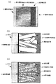
図6はGraetzel型の色素増感半導体電極を用いた光化学電池(以下、Graetzel型セルという。)の概略構成を示す模式的な断面図である。
【0008】
図6中64はガラス基板であり、65はその表面に形成した透明電極層であり、61はアナターゼ型多孔質酸化チタン層であり酸化チタン微粒子同士が接合したポーラス状の接合体からできている。また、62はその酸化チタン微粒子表面に接合させた色素であり光吸収層として作用する。
【0009】
次に、Graetzel型セルの製造方法について図6を用いて説明する。
【0010】
まず透明電極65が付いたガラス基板64aにアナターゼ型TiO2 微粒子61の膜を作製する。作製方法には各種があるが、一般的には20nm程度の微粒子径を有するアナターゼ型TiO2 微粒子を分散させたペーストを電極上に塗布し、350〜500℃で焼成して厚み約10μmのアナターゼ型TiO2 微粒子膜を作製する。この際微粒子同士程よく接合して、空孔度が50%程度でラスネスファクター(実質的な表面積/見かけ上の表面積)が1000程度の構造の膜が得られる。
【0011】
次にこの微粒子付き電極に色素を吸着させる。色素には各種の物質が検討されているが、一般的にはRu錯体などが利用される。この色素を溶かした溶液に電極を浸して乾燥させると、TiO2 微粒子の表面に光吸収層62が結合される。この溶媒には色素をよく溶解し、かつ色素の電極への吸着を阻害せず、仮に電極表面に残留していても電気化学的に不活性なエタノールやアセトニトリルなどが用いられる。
【0012】
次に対極としてやはり透明電極66が付いたガラス基板64bを用意し、表面に白金やグラファイトなどの超薄膜を形成する。この薄膜は酸化還元(レドックス)における電荷のやり取りの際の触媒として作用する。
【0013】
そして、電解液63を上記2つの電極65、66間に保持して重ねるとGraetzel型セルができあがる。電解液の溶媒としては電気化学的に不活性で、かつ電解質を充分な量溶解できるアセトニトリルや炭酸プロピレンなどが用いられる。また、電解質については安定なイオンのレドックス対であるI- /I3 -やBr- /Br3 -などが用いられる。例えば、I- /I3 -対をつくるときにはヨウ素のアンモニウム塩とヨウ素を混合する。
【0014】
その後、耐久性を持たせるため接着剤などでセルの封止をすることが好ましい。
【0015】
続いて、Graetzel型セルの動作原理について説明する。このGraetzel型セルに図6左側から光を入射させる。すると、入射光により光吸収層62を構成する色素中の電子が励起され、酸化チタンの伝導帯に移動する。電子を失って酸化状態にある色素は迅速に電解液63のヨウ素イオンから電子を受け取って還元され元の状態に戻る。酸化チタン層61に注入された電子は、酸化チタン微粒子の間をホッピング伝導などの機構により移動し透明電極層(アノード)65に到達する。また、色素に電子を供給して酸化状態(I3 -)になったヨウ素イオンは透明電極層(カソード)66から電子を受け取って還元され、元の状態(I- )に戻る。
【0016】
上記動作原理から推測できるように、色素で生成した電子とホールが効率良く分離、移動するためには、色素の励起状態の電子のエネルギー準位はTiO2 の伝導帯より高い必要があり、色素のホールのエネルギー準位はレドックス準位より低い必要性がある。
【0017】
この様なGraetzel型セルがシリコン太陽電池にとって代わるためには今まで以上に高いエネルギー変換効率や、さらに高い短絡電流、開放電圧、形状因子、耐久性が必要になってくる。
【0018】
【発明が解決しようとする課題】
しかしながら、上記従来技術の色素増感半導体電極は、チタニア微粒子を分散させた溶液を透明導電膜付きの基板上に塗布し、乾燥後に高温焼結して得られた酸化チタン膜を用いていたために、透明電極とチタニア微粒子の界面や、酸化チタン微粒子間の界面において電子伝導が散乱される傾向があった。このため透明導電膜と酸化チタン膜との界面、及び酸化チタン微粒子同士の界面に生じる内部抵抗が大きくなり、その結果光電変換効率が低下する原因となっていた。
【0019】
また、色素増感半導体電極が微粒子の焼結体で構成されていたため、透明電極近傍の微粒子には色素を吸着させるのに時間がかかり、また電解液中のイオンの拡散も遅いなどの課題があった。
【0020】
よって本発明の目的は、電子の授受がスムーズに行われ、変換効率が高い光電変換装置を提供することにある。
【0021】
また本発明の別の目的は、色素などの光吸収層や電解液などの電荷輸送層のしみ込みや移動が速い半導体電極を有する光電変換装置を提供することにある。
【0022】
また本発明の別の目的は、開放電圧が高い光電変換装置を提供することにある。
【0024】
【課題を解決するための手段】
上記の課題は本発明の光電変換装置により解決できる。
【0025】
すなわち、本発明の光電変換装置は、電子受容型の電荷輸送層と、電子供与型の電荷輸送層と、これらの電荷輸送層間に存在する光吸収層とを少なくとも有する光電変換装置であって、前記電子受容型及び電子供与型の電荷輸送層のいずれか一方が薄片状結晶から成る半導体層を含んでいることを特徴とするものである。
【0026】
また、本発明の光電変換装置は、電子受容型の電荷輸送層と、電子供与型の電荷輸送層と、これらの電荷輸送層間に存在する光吸収層とを少なくとも有する光電変換装置であって、前記電子受容型及び電子供与型の電荷輸送層のいずれか一方が少なくとも2種類以上の異なった様態もしくは組成の混合物から成る半導体層であり、且つ該混合物の少なくとも1種類が薄片状結晶であることを特徴とするものである。
【0027】
上記構成において、前記混合物中の薄片状結晶以外の半導体が直径100nm以下の微粒子であることが好ましく、前記微粒子が、薄片状結晶の表面に存在することがより良い。また、前記薄片状結晶の厚みと面の大きさに関するアスペクト比が10以上が好ましく、前記薄片状結晶が基板上の電極に対して厚み部位で接合していることがより良い。この薄片状結晶の厚みが500nm以下、できれば50nm以下であることが良く、前記薄片状結晶の面が平面であることが好ましい。また、前記光吸収材料が色素であり、前記薄片状物が金属酸化物、特に酸化チタン、酸化亜鉛で、酸化錫であることが好ましい。
【0028】
また、前記薄片状結晶の一部がアルミナ等からなる多数の微細孔を有する微細孔層の微細孔内に存在することが好ましい。
【0033】
【発明の実施の形態】
本発明にかかる光電変換装置の主たる特徴は、薄片状結晶もしくは混合結晶を電子受容型(n型)もしくは電子供与型(p型)の電荷輸送層に用いることである。薄片状結晶とは面と厚みを持った板状のものであり、欠陥の無い薄片状単結晶もしくは若干の欠陥や粒界を含む薄片状結晶からなっている。さらに、曲面を有する薄片や、花びら状、扇状のものも含む。また、混合結晶とは電荷輸送層のいずれかが少なくとも2種類以上の異なった様態もしくは組成の混合物から成る半導体層であり、且つ該半導体層の1種類以上が薄片状結晶を含んだ混合結晶を意味するものとする。
【0034】
また、薄片状結晶の厚さ及び面及び面の大きさについて図8に示した。ここで、面の大きさ82は面の重心83を通る最小長さである。この時、(面の大きさ)/(厚み)をアスペクト比とする。
【0035】
また混合結晶の様態についての例を図10(a)、(b)及び(c)に示した。それぞれ、薄片状結晶の周囲に粒子が付着しているもの(図10(a))、薄片状結晶の周囲に針状のものが付着しているもの(図10(b))、薄片状結晶の周囲に膜状のものが付着しているもの(図10(c))等からなっている。薄片状結晶及びその混合結晶の効果を説明する為に、本発明と従来のGraetzel型セルとを比較しながら説明する。
<本発明の光電変換装置の構成について>
まず本発明の構成について説明する。
【0036】
前述したGraetzel型セルを始めとする色素増感型セルでは、色素1層の光吸収率が十分ではないために、表面積を大きくして実質的な光吸収量を大きくしている。本発明は色素増感に限らず、光吸収率が十分ではないために表面積を大きくする構成の光電変換装置一般に広く利用可能である。この表面を大きくする方法には上記Graetzel型セルの様に微粒子を分散、接合させる方法が簡単ではあるが、電子の移動が十分効率的ではない問題がある。例えば上記Graetzel型セルにおいて酸化チタン半導体層61を有するアノードとなる透明電極層65側から光入射を行った場合と、カソードとなる透明電極層66側から光入射を行った場合を比較すると、前者の方が光電変換効率が良い場合が多い。これは単なる色素による光吸収量の差だけではなく、光吸収により励起された電子が酸化チタン半導体層61を移動してアノード透明電極65に到達する確率が、透明電極から光励起位置が離れるに従って低下していくことを示唆している。即ち、結晶粒界が多いGraetzel型セルでは十分効率的な電子移動が達成されていないことを示唆している。
【0037】
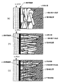
図1(a)〜(c)は本発明の光電変換装置の構成例を示す図である。図1において、10は電極付き基板、11は吸収層修飾薄片状混合結晶層、12は電荷輸送層、13は電極付き基板である。電極付き基板10は例えば透明電極層15が設けられたガラス基板14からなり、吸収層修飾薄片状混合結晶層11は半導体薄片状結晶17とその表面上に形成された光吸収層16とからなる。半導体薄片状結晶17は一方の電荷輸送層となり、この電荷輸送層と電荷輸送層12との間に光吸収層16が設けられることになる。
【0038】
本発明に用いる薄片状結晶層と微粒子結晶層を比較すると、薄片状結晶層の方が光励起により生成した電子もしくはホールが集電極へ移動するまでに粒界により散乱される確率が少なくなる。特に図1(b)に示した様に全ての薄片状結晶の一端が電極に接合された状態で構成されている場合には、電子もしくはホールの移動において、Graetzel型セルと比較すると、粒界の影響はほとんど解消される。また、薄片状結晶に違う種類の微結晶(半導体結晶18)が吸着している場合には、図1(c)に示した様に薄片状結晶のアスペクト比が小さい場合にもラフネスファクターを増大することができる。
【0039】
本発明にかかる光電変換装置では、薄片状結晶もしくは混合結晶はn型ワイドギャップ半導体もしくはp型ワイドギャップ半導体である。薄片状結晶もしくは混合結晶がn型ワイドギャップ半導体の場合には、色素の様な光吸収層16を挟んでp型のワイドギャップ半導体やレドックス対を含んだ電解液、高分子導電体などの電子供与型の電荷輸送層12が必要である。また、逆に薄片状結晶もしくは混合結晶がp型ワイドギャップ半導体の場合には、光吸収層16を挟んで電子受容型の電荷輸送層12が必要である。
【0040】
光の照射面はどの面に透明電極を用いるかによって決まる。図2(a)に示した構成はGraetzel型セルと同様に半導体結晶層側に透明電極を用いた例である。図2(b)に示した構成はそれとは逆の構成であり、光吸収層までの照射光の吸収や反射が少なければどちらの構成でも良い。また、図2(c)に示した様に、どちらの面からの光照射でも利用可能にできる構成もある。これらの構成は半導体薄片状結晶の作製方法、及び組み合わせる電荷輸送層の製法や組成に依存する。例えばPt膜上への電着による薄片状結晶の作製の場合には、薄片状結晶面からは光照射はできなくなる。薄片状結晶粉の焼成の様な低温プロセスで薄片状結晶面を作製する場合には透明電極層を劣化させずに作製できるので、どちらの面でも光照射面にできる。
【0041】
図9(a)、(b)は上記薄片状結晶及び混合結晶についての具体的な構成例を示す図である。図6に示したGraetzel型セルと比較すると、粒界の影響がほとんど解消されることにより電子及びホールの移動が容易にできる。さらに、図9(b)のように半導体結晶18が吸着することにより、粒界の影響が小さくラフネスファクターを向上させることができる。さらに、どの面に光を照射しても広範囲に照射光を到達させることができる。そのため、多くの電子移動が可能となり、変換効率のよい光電変換装置のセルを作製することができる。
【0042】
次に本発明に用いる薄片状結晶について説明する。
<薄片状結晶及び混合結晶について>
上記Graetzel型セルの様な1層あたりの吸収効率が低い光吸収層を用いるセルでは、表面積を大きくするために空孔度が大きい微粒子膜を利用してラフネスファクターを増大させているが、薄片状結晶を用いても、そのアスペクト比が大きければラフネスファクターも増大でき、さらに平面を形成した薄片状結晶を厚み部位で接合させることにより、結晶粒界が少ない効率的な電子移動を成すことができる。光吸収率にも依存するが、少なくとも薄片状結晶のアスペクト比は5以上、できれば10以上、さらに100以上が好ましい。また薄片状結晶の厚みも500nm以下であること、できれば50nm以下が好ましい。
【0043】
また、薄片状結晶及び混合結晶としてはエネルギーギャップが大きなものが好ましく、具体的にはエネルギーギャップが3eV以上のものが好ましい。電子受容型(n型)結晶としては、例えばTiO2 、ZnO、SnO2 などが好ましく、電子供与型(p型)結晶としては例えばNiO、CuIなどが挙げられる。
【0044】
このような薄片状結晶の作製方法としては、薄片状結晶粉を上記Graetzel型セル同様に塗布、焼成させる方法がある。この場合、薄片状結晶が図3(a)の様に基板14と平行に重なってしまう状態より、図3(b)や図1(b)に見られる様に薄片状結晶の厚み部位が透明電極15に接合させた状態で、基板14と垂直方向に形成されている方が好ましい。また、薄片状結晶の面部位は、平面が好ましい。また、混合結晶において半導体結晶18は、あらかじめ混合した状態で塗布する方法と、1種類以上の半導体結晶を先に塗布してから重ね塗りするように塗布する方法がある。このとき、半導体結晶18の直径が100nm以下、できれば20nm以下の微粒子が好ましい。また、半導体結晶18は薄片状結晶の表面に存在することが好ましい。
【0045】
また基板上において薄片状結晶を成長させる方法も挙げられるが、この方法にも大きく分けて2種類ある。一つは結晶成分を外部から供給する方法であり、CVD法やPVD法、電着などが挙げられる。もうひとつの方法としては基板上の成分を反応させて薄片状結晶を成長させる方法がある。
【0046】
前者としては、例えば図5(a)に示した様に基板41上に金属層を成膜した後、TiO2 やZnOなどを大気開放型のCVD法を用いて金属層上に薄片状結晶成長させる方法や、図5(b)に示した様に金属基板自身に大気開放型のCVD法を用いて薄片状結晶成長させる方法が挙げられる。混合結晶に関しては、その後異なる半導体結晶18を塗布する方法が挙げられる。
【0047】
後者として例えば図5(a)に示した様にTiやZnなどの金属層を基板に成膜した後、酸化させて薄片状結晶成長させる方法や、図5(b)に示した様に金属基板自身を酸化させて薄片状結晶成長させる方法が挙げられる。
【0048】
また特に薄片状結晶の厚さや面の広さや成長方向を制御する方法として、図4に示した様なナノホールから薄片状結晶を成長させる方法がある。具体的には下地に金属層42もしくは金属基板44を設け、その上部にアルミ層を0.1〜数μm程度設け、上部アルミ層を陽極酸化させ微細孔層となるナノホール層43とする。この陽極酸化では蓚酸、りん酸、硫酸などが利用され、ナノホールの間隔は陽極酸化電圧で制御できる。また、ナノホール径は陽極酸化後にりん酸溶液などでエッチングすることにより制御できる。このアルミナナノホールを作製した後、薄片状結晶成分のめっき浴中で電解させると、アルミナナノホールの下地金属から半導体薄片状結晶17がナノホールを通して成長させ得る。電着による薄片状結晶の作製方法においては、一般的に電着条件が薄片状結晶の厚みや面の広さを決定する上で重要なファクターとなる。
【0049】
また、薄片状結晶の厚みや面の広さや成長方向を制御した後に、異なる形態又は種類の半導体結晶を用いたゲル溶液などに浸漬させる事により、図5に示した様に半導体薄片状結晶17の表面に半導体結晶18が存在する構造をとる事ができる。このことにより、薄片状結晶の表面積が不十分な場合でもラフネスファクターが大きい半導体結晶を作製する事ができ、且つ電子もしくはホールの移動において粒界の影響が少ない半導体薄片状結晶を作製する事ができる。
<光吸収層について>
本発明の光電変換装置の光吸収層としては、各種の半導体や色素が利用可能である。半導体としてはi型の光吸収係数が大きなアモルファス半導体や直接遷移型半導体が好ましい。色素としては金属錯体色素および/もしくはポリメチン色素、ペリレン色素、ローズベンガル、サンタリン(Santalin)色素、シアニン(Cyanin)色素などの有機色素や天然色素が好ましい。該色素は半導体微粒子の表面に対する適当な結合基を有していることが好ましい。好ましい結合基としては、COOH基、シアノ基、PO3 H2 基、または、オキシム、ジオキシム、ヒドロキシキノリン、サリチレートおよびαケトエノレートのようなπ伝導性を有するキレート化基が挙げられる。この中でもCOOH基、PO3 H2 基が特に好ましい。本発明に使用する色素が金属錯体色素の場合、ルテニウム錯体色素{Ru(dcbpy)2 (SCN)2 、(dcbpy=2,2−ビピリジン(bipyridine)−4,4′−ジカルボン酸(dicarboxylic acid)等}が利用できるが、酸化・還元体が安定であることが重要である。
【0050】
また、光吸収層の励起された電子の電位、即ち光励起した色素の電位(色素のLUMO電位)や半導体中の伝導帯電位が、電子受容型電荷輸送層の電子受容電位(n型半導体の伝導帯電位など)より高く、かつ光吸収層で光励起により生成したホール電位が、電子供与型電荷移動層の電子供与電位(p型半導体の価電子帯電位、レドックス対のポテンシャル電位など)より低いことが必要である。光吸収層近傍における励起された電子−ホールの再結合確率を低くすることも、光電変換効率を増大させる上で重要となる。
<電荷輸送層(薄片状結晶との対極)について>
n型の薄片状結晶を用いた場合、光吸収層を挟んでホール輸送層を作製する必要がある。このホール輸送層には湿式太陽電池同様レドックス系が利用可能である。レドックスを用いる場合でも単純な溶液系のみでなく、カーボンパウダーを保持材にしたり、電解質をゲル化する方法がある。また、溶融塩やイオン伝導性ポリマーを用いる方法もある。さらに電子(ホール)を輸送する方法として電界重合有機ポリマーやCuI、CuSCN、NiOなどのp型半導体を用いることもできる。逆にp型の薄片状結晶を用いた場合には、n型の半導体であるZnO、TiO2 、SnO2 などが利用可能となる。
【0051】
上記輸送層は薄片状結晶間に入り込む必要があるため、作製には液体や高分子などに利用できる浸透法や、固体の輸送層に利用できる電着、CVD法などが適している。
<電極について>
電荷輸送層、半導体薄片状結晶層に隣接するように電極が設けられる。電極はこれらの層の外側の前面に設けてもよいし一部に設けてもよい。電荷輸送層が固体でない場合、電荷輸送層を保持するという観点から前面に電極を設けたほうがよい。電荷輸送層に隣接する電極の表面には、例えばレドックス対の還元を効率よく行わせる為にPt、Cなどの触媒を設けておくことが好ましい。
【0052】
光入射側の電極としては、インジウム−スズ複合酸化物、酸化スズにフッ素をドープしたもの等からなる透明電極が好適に用いられる。光入射側の電極に接する層(電荷輸送層或いは半導体薄片状結晶層)の抵抗が十分低い場合には、光入射側の電極として部分的な電極、例えばフィンガー電極などを設けることも可能である。
【0053】
光入射側とはならない電極は、Cu、Ag、Al等からなる金属電極が好適に用いられる。
<基板について>
基板の材質、厚さは、光起電力装置に要求される耐久性に応じて適宜設計することができる。光入射側の基板は透光性である限り、ガラス基板、プラスチック基板などが好適に用いられる。光入射側とはならない基板としては、金属基板、セラミック基板などを適宜用いることができる。光入射側の基板の表面には、SiO2 などからなる反射防止膜を設けることが好ましい。
【0054】
なお、前述した電極に基板としての機能を兼ねさせることにより、電極とは別部材の基板を設けない様にしても良い。
<封止について>
図示してはないが、本発明の光電変換装置は少なくとも基板以外の部分を封止することが、耐候性を高める観点から好ましい。封止材としては接着剤や樹脂を用いることができる。なお、光入射側を封止する場合、封止材は透光性であることが好ましい。
【0055】
【実施例】
以下、実施例を用いて本発明をさらに説明する。
[実施例1]
本実施例は、ルチル型薄片状結晶粉を電子受容型電子輸送層に利用して光電変換装置を作製した例について図1を用いて説明する。
【0056】
厚みが50〜100nm、面の大きさが厚みの約10倍であるルチル型TiO2 薄片状結晶6g(グラム)を水10mL(ミリリットル)、アセチルアセトン0.2mL、トリトン−X(登録商標名;ユニオン・カーバイド社製)0.2mLと混合しスラリー状にした。
【0057】
このスラリーを導電性ガラス(FドープSnO2 、10Ω/□)上に、スペーサーを用いて厚み約50μm、1cm角に塗布した。そして酸素ガスを100mL/min(sccm)流しながら450℃で1時間焼成を行った。焼成後のTiO2 薄片状結晶層の膜厚は約10μmであった。色素はGraetzelらが報告しているRu錯体であるRu((bipy)(COOH)2 )2 (SCN)2 を用いた。色素を蒸留エタノールに溶解し、この中にTiO2 電極を120分浸して色素を電極に吸着させた後取りだし、80℃で乾燥させた。また、導電性ガラス(FドープSnO2 、10Ω/□)上に白金を1nm厚にスパッタ成膜した対極を用い、レドックス対はI- /I3 -を用いた。溶質はテトラプロピルアンモニウムヨウ化物(tetrapropylammonium iodide)(0.46mol/L)とヨウ素(0.06mol/L)、溶媒はエチレンカルボナート(ethylene carbonate)(80vol%)とアセトニトリル(acetonitrile)(20vol%)の混合液を用いた。この混合液をTiO2 付き導電性ガラスに滴下し、対極で挟んでセルとした。
【0058】
また、比較例として粒径約1μmを主成分としたTiO2 粉末を熱処理したものを用いて同様にセルを組み立てた。
【0059】
そして紫外線カットフィルターを取り付けた500Wのキセノンランプ光をTiO2 付き導電性ガラス側、もしくは対極側から照射した。そしてこの時生じた光電変換反応による光電流の値を測定した。その測定結果によると、本発明のセルの方が開放電位、フィルファクターともに5%程度大きく、特に対極側から光照射した場合には7%以上大きかった。これは薄片状結晶を用いたことによって電子受容型電荷輸送層の内部抵抗が減少したことに起因すると考えられる。
[実施例2]
本実施例では、実施例1のTiO2 薄片状結晶に変えてZnO薄片状結晶、およびSnO2 薄片状結晶をそれぞれ用いて実施例1と同様な光電変換装置を作製した。
【0060】
この際ZnO薄片状結晶は厚みが100〜200nm、面の大きさが厚みの約10倍であり、SnO2 薄片状結晶では厚みが100〜200nm、面の大きさが厚みの約10倍であった。製造方法はいずれも実施例1の素子と同様として、実施例1同様の評価を行った。その結果いずれの装置でも比較例(ZnO粉末を用いた装置、及びSnO2 粉末を用いた装置)と比べて、薄片状結晶層付き導電性ガラス側から光を照射した場合には、開放電位、フィルファクターともに3%程度大きく、対極側から光照射した場合には、開放電位、フィルファクターともに5%以上大きかった。これは薄片状結晶を用いたことによって電子受容型電荷輸送層の内部抵抗が減少したことに起因すると考えられる。
[実施例3]
本実施例は、電着によりナノホールから半導体薄片状結晶を作製した例について図4を用いて説明する。
【0061】
導電性ガラス基板(FドープSnO2 、10Ω/□)を用意し、表面にAlを0.5μm成膜した。そしてAl層を蓚酸0.3mol/L中で40Vにて陽極酸化させた後、りん酸5wt.%中に40分浸した。この処理により陽極酸化されたアルミナ層43には、約50nmの径のナノホールが約100nm間隔で多数開いていた。次に、この基板を作用極として0.1mol/L硝酸亜鉛水溶液に浸し、−2Vの電位を5000秒間印加を行った。電解後、基板表面にはアルミナナノホールからZnO薄片状結晶17が電極から図4(a)、(b)に示した様に成長していた。このZnO薄片状結晶の厚みは5〜10nmであり、面の大きさはその50〜200倍であった。そして実施例1と同様に薄片状結晶の表面に色素を吸着させた。そして、導電性ガラス(FドープSnO2 、10Ω/□)上にグラファイトを約1nm厚に形成した対極を用い、レドックス対としてI- /I3 -を用いた。溶質も実施例1と同様にテトラプロピルアンモニウムヨウ化物(tetrapropylammonium iodide)(0.46mol/L)とヨウ素(0.06mol/L)、溶媒はエチレンカルボナート(ethylene carbonate)(80vol%)とアセトニトリル(acetonitrile)(20vol%)の混合液を用いた。この混合液をZnO 付き導電性ガラスに滴下し、対極で挟んでセルとした。
【0062】
また、比較例として粒径1μmを主成分としたZnO 粉末を熱処理したものを用いて同様にセルを組み立てた。
【0063】
そして実施例1と同様に紫外線カットフィルターを取り付けた500Wのキセノンランプ光を対極側から照射した。そしてこの時生じた光電変換反応による光電流の値を測定した。その測定結果本発明のセルの方が開放電位、フィルファクターともに9%程度大きかった。これは薄片状結晶を用いたことによって電子受容型電荷輸送層の内部抵抗が減少したことに起因すると考えられる。
[実施例4]
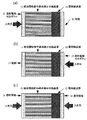
本実施例は、大気開放型CVD法を用いて半導体薄片状結晶を作製した例について図5及び図7を用いて説明する。
【0064】
石英基板41上にAl下地金属層42を3μm成膜した基板、及びAl板44の基板を用意し、それぞれCVD装置の基板加熱台76に設置した。そして、原料気化器73に固体状のチタン(IV)イソプロポキシドを入れ、130℃の熱を加えて気化させた。それを窒素で運んでノズル74から加熱したAl基板75上に吹き付けた。処理後のAl下地、及びAl基板表面にはTiO2 薄片状結晶が基板から図5(a)、(b)に示した様に成長していた。このTiO2 薄片状結晶の厚みは50〜100nmであり、面の大きさはその20〜100倍であった。その基板を、粒径約20nmのアナターゼ型TiO2 微結晶(P25)3gを水40mL、アセチルアセトン0.2mL、トリトン−X0.2mLと混合しスラリー状にした溶液内に浸漬させ、さらに酸素を100mL/min(sccm)流しながら450℃で1時間焼成を行った。
【0065】
そして実施例1同様に混合結晶の表面に色素を吸着させた。そして、導電性ガラス(FドープSnO2 、10Ω/□)上にグラファイトを約1nm厚に形成した対極を用い、レドックス対としてI- /I3 -を用いた。溶質も実施例1同様テトラプロピルアンモニウムヨウ化物(tetrapropylammonium iodide)(0.46mol/L)とヨウ素(0.06mol/L)、溶媒はエチレンカルボナート(ethylene carbonate)(80vol%)とアセトニトリル(acetonitrile)(20vol%)の混合液を用いた。この混合液をTiO2 付き導電性基板に滴下し、対極で挟んでセルとした。
【0066】
また、比較例として粒径約1μmを主成分としたTiO2 粉末を熱処理したものを用いて同様にセルを組み立てた。
【0067】
そして実施例1と同様に紫外線カットフィルターを取り付けた500Wのキセノンランプ光を対極側から照射した。そしてこの時生じた光電変換反応による光電流の値を測定した。その測定結果本発明のセルの方が開放電位、フィルファクターともに7%程度大きかった。これは薄片状結晶を用いたことによって電子受容型電荷輸送層の内部抵抗が減少したことに起因すると考えられる。
[実施例5]
本実施例は、電着により基板から半導体薄片状結晶を作製した例について図5を用いて説明する。
【0068】
ガラス基板41上にPt下地基板42を1μm成膜した基板を用意した。次に、この基板を作用極として0.1mol/L硝酸亜鉛水溶液に浸し、−2Vの電位を5000秒間印加を行った。電解後、基板表面にはZnO 薄片状結晶17が電極から図5(a)に示した様に成長していた。このZnO 薄片状結晶の厚みは50〜100nmであり、面の大きさはその20〜200倍であった。その基板を、粒径約20nmのアナターゼ型TiO2 微結晶(P25)3gを水40mL、アセチルアセトン0.2mL、トリトン−X0.2mLと混合しスラリー状にした溶液内に浸漬させ、さらに酸素を100mL/min(sccm)流しながら450℃で1時間焼成を行った。そして実施例1同様に混合結晶の表面に色素を吸着させた。そして、導電性ガラス(FドープSnO2 、10Ω/□)上にグラファイトを約1nm厚に形成した対極を用い、p−型半導体としてCuIを使用した。CuIは、無水のアセトニトリルに溶解し、色素を担持したメソスコピックZnO膜界面に析出させた。このようにして調整した固体電極を対極と重ね合せて固体化太陽電池を作製した。
【0069】
また、比較例として粒径約1μmを主成分としたZnO 粉末を熱処理したものを用いて同様にセルを組み立てた。
【0070】
そして実施例1同様に紫外線カットフィルターを取り付けた500Wのキセノンランプ光を対極側から照射した。そしてこの時生じた光電変換反応による光電流の値を測定した。その測定結果本発明のセルの方が開放電位、フィルファクターともに9%程度大きかった。これは薄片状結晶を用いたことによって電子受容型電荷輸送層の内部抵抗が減少したことに起因すると考えられる。
[実施例6]
本実施例は、ルチル型薄片状結晶粉を電子受容型電子輸送層に利用して光電変換装置を作製した例について図3を用いて説明する。
【0071】
厚みが50〜100nm、面の大きさが厚みの約10倍であるルチル型TiO2 薄片状結晶6gを水10mL、アセチルアセトン0.2mL、トリトン−X0.2mLと混合しスラリー状にした。
【0072】
このスラリーを導電性ガラス(FドープSnO2 、10Ω/□)上に、スペーサーを用いて厚み約50μm、1cm角に塗布した。そして酸素ガスを100mL/min(sccm)流しながら450℃で1時間焼成を行った。焼成後のTiO2 薄片状結晶層の膜厚は約10μmであった。その基板を、粒径約20nmのアナターゼ型TiO2 微結晶(P25)3gを水40mL、アセチルアセトン0.2mL、トリトン−X0.2mLと混合しスラリー状にした溶液内に浸漬させ、さらに酸素を100mL/min(sccm)流しながら450℃で1時間焼成を行った。そして実施例1同様に混合結晶の表面に色素を吸着させた。そして、導電性ガラス(FドープSnO2 、10Ω/□)上にPtを約1nm厚に形成した対極を用い、レドックス対としてI- /I3 -を用いた。溶質も実施例1同様テトラプロピルアンモニウムヨウ化物(tetrapropylammonium iodide)(0.46mol/L)とヨウ素(0.06mol/L)、溶媒はエチレンカルボナート(ethylene carbonate)(80vol%)とアセトニトリル(acetonitrile)(20vol%)の混合液を用いた。この混合液をTiO2 付き導電性ガラスに滴下し、対極で挟んでセルとした。
【0073】
また、比較例として粒径約1μmを主成分としたTiO2粉末を熱処理したものを用いて同様にセルを組み立てた。
【0074】
そして紫外線カットフィルターを取り付けた500Wのキセノンランプ光をTiO2 付き導電性ガラス側、もしくは対極側から照射した。そしてこの時生じた光電変換反応による光電流の値を測定した。その測定結果本発明のセルの方が開放電位、フィルファクターともに3%程度大きく、特に対極側から光照射した場合には5%以上大きかった。これは薄片状結晶を用いたことによって電子受容型電荷輸送層の内部抵抗が減少したことに起因すると考えられる。
【0075】
【発明の効果】
以上説明したように本発明によれば、電子やホールの授受及び移動がスムーズに行われ、内部抵抗や再結合確率が低く、変換効率が高い光電変換装置を提供することができる。
【0076】
また本発明によれば、色素などの光吸収層や電解液などの電荷輸送層のしみ込みや移動が速い半導体電極を有する光電変換装置を提供することができる。
【0077】
また本発明によれば、開放電圧が高い光電変換装置を提供することができる。
【図面の簡単な説明】
【図1】本発明の光電変換装置を示す断面概略図である。
【図2】本発明の光照射と透明電極、薄片状結晶層の構成例を示す断面図である。
【図3】本発明の薄片状結晶の接合状態を示す断面図である。
【図4】本発明のナノホールからの薄片状結晶を示す断面図である。
【図5】本発明の基板からの薄片状結晶を示す断面図である。
【図6】従来例のGraetzel型セルを示す断面図である。
【図7】大気開放型CVD装置の簡略図である。
【図8】薄片状結晶の簡略図である。
【図9】針状及び混合結晶を用いたセルを示す断面図である。
【図10】混合結晶の様態を示す断面図である。
【符号の説明】
10 電極付き基板
11 吸収層修飾半導体薄片状結晶層
12 電荷輸送層
13 電極付き基板
14 ガラス
15 透明電極層
16 光吸収層
17 半導体薄片状結晶
18 半導体結晶
21 透明電極付きガラス
22 電極
41 基板
42 下地電極層
43 ナノホール層
44 下地電極
61 アナターゼ型TiO2 微粒子
62 光吸収層
63 電解液
64 ガラス
65 透明電極層(アノード)
66 透明電極層(カソード)
71 窒素ボンベ
72 流量計
73 原料気化器
74 ノズル
75 基板
76 基板加熱台
81 面
82 面の大きさ
83 厚み
83 面の重心[0001]
BACKGROUND OF THE INVENTION
The present invention relates to a photoelectric conversion device, in particular an electron acceptor type charge-transporting layer, a charge transport layer of the electron donor type, a photoelectric conversion device having at least a light absorbing layer present in these charge transport layers.
[0002]
[Prior art]
As a method for converting light energy into electric energy, a solar cell using a semiconductor junction such as silicon or gallium-arsenic is generally used. Among them, single crystal silicon solar cells using polycrystalline semiconductor pn junctions, polycrystalline silicon solar cells, and amorphous silicon solar cells using pin junctions are well known and are being put into practical use. However, since silicon solar cells are expensive to manufacture and consume a lot of energy in the manufacturing itself, long-term use is required to recover the introduction cost and energy consumption. This cost is mainly the bottleneck of the current spread.
[0003]
On the other hand, research on practical application of CdTe, CuIn (Ga) Se, etc. as a second generation thin film solar cell has been progressing recently, but environmental problems and resource problems have been raised in these material systems.
[0004]
As a method other than the above semiconductor bonding, a wet solar cell using a photoelectrochemical reaction that occurs at the interface between a semiconductor and an electrolyte solution has been reported. Metal oxide semiconductors such as titanium oxide and tin oxide used in this wet solar cell can be manufactured at a lower cost than silicon and gallium arsenide used in the dry solar cell. Titanium is expected as a future energy conversion material because it is excellent in both photoelectric conversion characteristics and stability. However, since stable optical semiconductors such as titanium oxide have a wide band gap of 3 eV or more, only ultraviolet light that is about 4% of sunlight can be used, and it cannot be said that the conversion efficiency is sufficiently high.
[0005]
Then, the photochemical cell (dye-sensitized solar cell) which adsorb | sucked the pigment | dye on the surface of this optical semiconductor was researched. In the early days, semiconductor single crystal electrodes have been used. Examples of the electrode include titanium oxide, zinc oxide, cadmium sulfide, and tin oxide. However, since the single crystal electrode has a low efficiency due to the small amount of dye adsorbed, an attempt has been made to make the semiconductor electrode porous. Tsubomura et al. Reported that the efficiency was improved by adsorbing a dye to a semiconductor electrode made of porous zinc oxide obtained by sintering fine particles (NATURE, 261 (1976) p402). Proposals regarding the use of a porous semiconductor electrode have been made in Japanese Patent Application Laid-Open Nos. 10-112337 and 9-237641.
[0006]
In addition, Graetzel et al. Reported that the dye and the semiconductor electrode were further improved to obtain the same performance as a silicon solar cell (J. Am. Chem. Soc. 115 (1993) 6382, US Pat. No. 5,350,644). ). Here, a ruthenium dye is used as the dye, and anatase type porous titanium oxide (TiO 2 ) is used as the semiconductor electrode.
[0007]
FIG. 6 is a schematic cross-sectional view showing a schematic configuration of a photochemical battery (hereinafter referred to as a Graetzel type cell) using a Graetzel type dye-sensitized semiconductor electrode.
[0008]
In FIG. 6, 64 is a glass substrate, 65 is a transparent electrode layer formed on the surface, 61 is an anatase type porous titanium oxide layer, and is made of a porous joined body in which titanium oxide fine particles are joined together. . Reference numeral 62 denotes a dye bonded to the surface of the titanium oxide fine particles and functions as a light absorption layer.
[0009]
Next, a method for manufacturing a Graetzel type cell will be described with reference to FIG.
[0010]
First, a film of anatase TiO 2 fine particles 61 is formed on a glass substrate 64a with a transparent electrode 65. There are various production methods. Generally, a paste in which anatase-type TiO 2 fine particles having a fine particle diameter of about 20 nm are dispersed is applied on an electrode and baked at 350 to 500 ° C., and anatase having a thickness of about 10 μm. Type TiO 2 fine particle film is prepared. At this time, the fine particles are joined to each other well, and a film having a structure with a porosity of about 50% and a roughness factor (substantial surface area / apparent surface area) of about 1000 is obtained.
[0011]
Next, a dye is adsorbed on the electrode with fine particles. Various substances have been studied for the dye, but Ru complexes are generally used. When the electrode is immersed in a solution in which the dye is dissolved and dried, the light absorption layer 62 is bonded to the surface of the TiO 2 fine particles. In this solvent, ethanol or acetonitrile, which dissolves the dye well and does not inhibit the adsorption of the dye to the electrode and is electrochemically inert even if it remains on the electrode surface, is used.
[0012]
Next, a glass substrate 64b with a transparent electrode 66 is prepared as a counter electrode, and an ultra-thin film such as platinum or graphite is formed on the surface. This thin film acts as a catalyst in charge exchange in redox.
[0013]
Then, when the electrolytic solution 63 is held between the two electrodes 65 and 66 and stacked, a Graetzel type cell is completed. As the solvent of the electrolytic solution, acetonitrile, propylene carbonate, or the like that is electrochemically inactive and can dissolve a sufficient amount of the electrolyte is used. As the electrolyte, I − / I 3 − or Br − / Br 3 − which is a stable redox pair of ions is used. For example, when making an I − / I 3 − pair, an ammonium salt of iodine and iodine are mixed.
[0014]
After that, it is preferable to seal the cells with an adhesive or the like in order to provide durability.
[0015]
Next, the operation principle of the Graetzel type cell will be described. Light enters the Graetzel type cell from the left side of FIG. Then, the electrons in the dye constituting the light absorption layer 62 are excited by the incident light and move to the conduction band of titanium oxide. The dye that has lost electrons and is in an oxidized state quickly receives electrons from iodine ions in the electrolytic solution 63 and is reduced to return to the original state. The electrons injected into the titanium oxide layer 61 move between the titanium oxide fine particles by a mechanism such as hopping conduction and reach the transparent electrode layer (anode) 65. In addition, iodine ions that are in an oxidized state (I 3 − ) by supplying electrons to the dye receive electrons from the transparent electrode layer (cathode) 66 and are reduced to return to the original state (I − ).
[0016]
As can be inferred from the above operating principle, in order for the electrons and holes generated in the dye to be efficiently separated and moved, the energy level of the excited electron of the dye must be higher than the conduction band of TiO 2. The energy level of the hole must be lower than the redox level.
[0017]
In order for such a Graetzel type cell to replace a silicon solar cell, higher energy conversion efficiency, higher short-circuit current, open-circuit voltage, form factor, and durability are required.
[0018]
[Problems to be solved by the invention]
However, the dye-sensitized semiconductor electrode of the above prior art uses a titanium oxide film obtained by applying a solution in which titania fine particles are dispersed on a substrate with a transparent conductive film and drying at a high temperature after drying. Electron conduction tended to be scattered at the interface between the transparent electrode and the titania fine particles or at the interface between the titanium oxide fine particles. For this reason, the internal resistance which arises in the interface of a transparent conductive film and a titanium oxide film, and the interface of titanium oxide microparticles | fine-particles became large, and it became the cause for photoelectric conversion efficiency falling as a result.
[0019]
In addition, since the dye-sensitized semiconductor electrode is composed of a sintered body of fine particles, it takes time to adsorb the dye to the fine particles in the vicinity of the transparent electrode, and the diffusion of ions in the electrolytic solution is slow. there were.
[0020]
Accordingly, an object of the present invention is to provide a photoelectric conversion device in which electrons are exchanged smoothly and conversion efficiency is high.
[0021]
Another object of the present invention is to provide a photoelectric conversion device having a semiconductor electrode in which a light absorption layer such as a dye or a charge transport layer such as an electrolytic solution penetrates or moves quickly.
[0022]
Another object of the present invention is to provide a photoelectric conversion device having a high open circuit voltage.
[0024]
[Means for Solving the Problems]
The above problems can be solved by the photoelectric conversion device of the present invention.
[0025]
That is, the photoelectric conversion device of the present invention is a photoelectric conversion device having at least an electron-accepting charge transport layer, an electron-donating charge transport layer, and a light absorption layer present between these charge transport layers, wherein in which one of the electron acceptor-type and electron donating charge transport layer is characterized in that it comprises a semiconductor layer made of flaky crystals.
[0026]
The photoelectric conversion device of the present invention is a photoelectric conversion device having at least an electron-accepting charge transport layer, an electron-donating charge transport layer, and a light absorption layer present between these charge transport layers, wherein one of the electron acceptor-type and electron donating charge transport layer is a semiconductor layer consisting of at least two types of differentiated state or a mixture of the composition, and that at least one of the mixture is a flaky crystals It is characterized by.
[0027]
In the above configuration, the semiconductor other than the flaky crystals in the mixture is preferably fine particles having a diameter of 100 nm or less, and the fine particles are more preferably present on the surface of the flaky crystals. Further, the aspect ratio regarding the thickness and the surface size of the flaky crystal is preferably 10 or more, and the flaky crystal is more preferably bonded to the electrode on the substrate at the thickness portion. The thickness of the flaky crystal is preferably 500 nm or less, preferably 50 nm or less, and the plane of the flaky crystal is preferably a flat surface. Further, it is preferable that the light absorbing material is a pigment, and the flaky material is a metal oxide, particularly titanium oxide or zinc oxide, and is tin oxide.
[0028]
Moreover, it is preferable that a part of the flaky crystal is present in the micropores of a microporous layer having a large number of micropores made of alumina or the like.
[0033]
DETAILED DESCRIPTION OF THE INVENTION
The main feature of the photoelectric conversion device according to the present invention is that a flaky crystal or a mixed crystal is used for an electron-accepting (n-type) or electron-donating (p-type) charge transport layer. The flaky crystal is a plate having a surface and a thickness, and is composed of a flaky single crystal having no defect or a flaky crystal containing some defects and grain boundaries. Further, it includes a flake having a curved surface, a petal shape, and a fan shape. A mixed crystal is a semiconductor layer in which one of the charge transport layers is made of a mixture of at least two or more different modes or compositions, and at least one of the semiconductor layers is a mixed crystal containing flaky crystals. Shall mean.
[0034]
Further, FIG. 8 shows the thickness, face, and face size of the flaky crystals. Here, the surface size 82 is the minimum length passing through the center of gravity 83 of the surface. At this time, (surface size) / (thickness) is defined as the aspect ratio.
[0035]
Examples of mixed crystal modes are shown in FIGS. 10 (a), (b), and (c). In each case, particles are attached around the flaky crystals (FIG. 10A), needles are attached around the flaky crystals (FIG. 10B), and flaky crystals. And the like (FIG. 10 (c)) and the like in which a film-like material adheres to the periphery. In order to explain the effect of the flaky crystals and mixed crystals thereof, the present invention will be described while comparing with a conventional Graetzel type cell.
<Regarding Configuration of Photoelectric Conversion Device of the Present Invention>
First, the configuration of the present invention will be described.
[0036]
In the dye-sensitized cells such as the above-described Graetzel type cell, the light absorption rate of one layer of the dye is not sufficient. Therefore, the surface area is increased to increase the substantial light absorption amount. The present invention is not limited to dye sensitization, and can be widely used for general photoelectric conversion devices having a configuration in which the surface area is increased because the light absorption rate is not sufficient. This method of enlarging the surface has a problem that the movement of electrons is not sufficiently efficient, although the method of dispersing and bonding fine particles is simple as in the Graetzel type cell. For example, in the Graetzel type cell, when comparing the case where light is incident from the transparent electrode layer 65 side serving as the anode having the titanium oxide semiconductor layer 61 and the case where light is incident from the transparent electrode layer 66 side serving as the cathode, the former In many cases, the photoelectric conversion efficiency is better. This is not only a difference in the amount of light absorption by the dye, but also the probability that electrons excited by light absorption move through the titanium oxide semiconductor layer 61 and reach the anode transparent electrode 65 as the photoexcitation position moves away from the transparent electrode. It is suggested to do. That is, it is suggested that a sufficiently efficient electron transfer is not achieved in a Graetzel type cell with many crystal grain boundaries.
[0037]
1A to 1C are diagrams illustrating a configuration example of a photoelectric conversion device of the present invention. In Figure 1, 1 0 the electrode-attached substrate, 11 is absorbed layer modified flaky mixed crystal layer, 12 is a charge-transporting layer, 13 is an electrode-attached substrate. Consists substrate with electrode 1 0 a glass substrate 14, for example a transparent electrode layer 15 is provided, the absorbent layer modified flaky mixed crystal layer 11 is a semiconductor flaky crystals 17 and the light absorbing layer 16 formed on the surface thereof Become. The semiconductor flaky crystal 17 becomes one charge transport layer, and the light absorption layer 16 is provided between the charge transport layer and the charge transport layer 12.
[0038]
When the flaky crystal layer and the fine particle crystal layer used in the present invention are compared, the probability that the flaky crystal layer is scattered by the grain boundary before electrons or holes generated by photoexcitation moves to the collector electrode is reduced. In particular, as shown in FIG. 1B, when one end of every flaky crystal is configured to be joined to an electrode, the grain boundary is smaller in the movement of electrons or holes than in the Graetzel type cell. The effects of are almost eliminated. In addition, when different types of microcrystals (semiconductor crystal 18) are adsorbed on the flaky crystals, the roughness factor is increased even when the aspect ratio of the flaky crystals is small as shown in FIG. 1 (c). can do.
[0039]
In the photoelectric conversion device according to the present invention, the flaky crystal or mixed crystal is an n-type wide gap semiconductor or a p-type wide gap semiconductor. When the flaky crystal or mixed crystal is an n-type wide gap semiconductor, an electron such as a p-type wide gap semiconductor, an electrolyte containing a redox pair, a polymer conductor, etc. sandwiching a light absorption layer 16 such as a dye. A donor type charge transport layer 12 is required. Conversely, when the flaky crystal or mixed crystal is a p-type wide gap semiconductor, the electron-accepting charge transport layer 12 is necessary with the light absorption layer 16 in between.
[0040]
The light irradiation surface is determined by the surface on which the transparent electrode is used. The configuration shown in FIG. 2A is an example in which a transparent electrode is used on the semiconductor crystal layer side as in the Graetzel type cell. The configuration shown in FIG. 2B is the opposite configuration, and either configuration may be used as long as there is little absorption or reflection of irradiation light to the light absorption layer. In addition, as shown in FIG. 2C, there is a configuration that can be used by light irradiation from either surface. These configurations depend on the method for producing the semiconductor flaky crystal and the production method and composition of the charge transport layer to be combined. For example, in the case of producing a flaky crystal by electrodeposition on a Pt film, light cannot be irradiated from the flaky crystal surface. When a flaky crystal surface is produced by a low-temperature process such as baking of flaky crystal powder, the transparent electrode layer can be produced without deteriorating, so that either surface can be a light irradiation surface.
[0041]
FIGS. 9A and 9B are diagrams showing specific configuration examples of the flaky crystal and the mixed crystal. Compared with the Graetzel type cell shown in FIG. 6, the movement of electrons and holes can be facilitated by almost eliminating the influence of grain boundaries. Furthermore, as shown in FIG. 9B, the semiconductor crystal 18 is adsorbed, so that the influence of the grain boundary is small and the roughness factor can be improved. Furthermore, irradiation light can reach a wide range regardless of which surface is irradiated with light. Therefore, a large number of electrons can be moved, and a cell of a photoelectric conversion device with high conversion efficiency can be manufactured.
[0042]
Next, the flaky crystal used in the present invention will be described.
<About flaky crystals and mixed crystals>
In a cell using a light absorption layer having a low absorption efficiency per layer such as the Graetzel type cell, the roughness factor is increased by using a fine particle film having a large porosity in order to increase the surface area. Even if crystal-like crystals are used, the roughness factor can be increased if the aspect ratio is large, and more efficient electron transfer with few crystal grain boundaries can be achieved by joining flaky crystals with a flat surface at the thickness site. it can. Although depending on the light absorption rate, at least the aspect ratio of the flaky crystals is preferably 5 or more, preferably 10 or more, and more preferably 100 or more. The thickness of the flaky crystal is preferably 500 nm or less, and preferably 50 nm or less.
[0043]
Further, the flaky crystal and the mixed crystal preferably have a large energy gap, and specifically, those having an energy gap of 3 eV or more are preferable. As the electron accepting (n-type) crystal, for example, TiO 2 , ZnO, SnO 2 and the like are preferable, and as the electron donating (p-type) crystal, for example, NiO, CuI and the like can be mentioned.
[0044]
As a method for producing such flaky crystals, there is a method in which flaky crystal powder is applied and fired in the same manner as the Graetzel type cell. In this case, since the flaky crystal overlaps with the substrate 14 in parallel as shown in FIG. 3A, the thickness portion of the flaky crystal is transparent as seen in FIGS. 3B and 1B. It is preferable that the electrode 15 is formed in a direction perpendicular to the substrate 14 while being bonded to the electrode 15. The plane part of the flaky crystal is preferably a flat surface. Further, in the mixed crystal, there are a method of applying the semiconductor crystal 18 in a premixed state, and a method of applying one or more types of semiconductor crystals so as to be overcoated. At this time, fine particles having a diameter of the semiconductor crystal 18 of 100 nm or less, preferably 20 nm or less are preferable. The semiconductor crystal 18 is preferably present on the surface of the flaky crystal.
[0045]
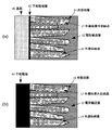
Moreover, although the method of growing a flaky crystal on a substrate is also mentioned, there are roughly two types of this method. One is a method of supplying a crystal component from the outside, and examples thereof include a CVD method, a PVD method, and electrodeposition. As another method, there is a method of growing flaky crystals by reacting components on the substrate.
[0046]
As the former, for example, as shown in FIG. 5A, after forming a metal layer on the substrate 41, TiO 2 or ZnO or the like is grown on a flaky crystal on the metal layer by using the open-air CVD method. And a method of growing flaky crystals on the metal substrate itself by using an open-air CVD method as shown in FIG. 5B. As for the mixed crystal, a method of applying a different semiconductor crystal 18 thereafter can be mentioned.
[0047]
As the latter, for example, as shown in FIG. 5 (a), a metal layer such as Ti or Zn is formed on a substrate and then oxidized to flaky crystal growth, or a metal layer as shown in FIG. 5 (b). An example is a method in which the substrate itself is oxidized to grow a flaky crystal.
[0048]
In particular, as a method for controlling the thickness, surface area, and growth direction of the flaky crystals, there is a method of growing flaky crystals from nanoholes as shown in FIG. Specifically, a metal layer 42 or a metal substrate 44 is provided on the base, an aluminum layer is provided on the upper part thereof in an amount of about 0.1 to several μm, and the upper aluminum layer is anodized to form a nanohole layer 43 that becomes a microporous layer. In this anodic oxidation, oxalic acid, phosphoric acid, sulfuric acid or the like is used, and the nanohole interval can be controlled by the anodic oxidation voltage. The nanohole diameter can be controlled by etching with a phosphoric acid solution after anodization. When this alumina nanohole is produced and then electrolyzed in a plating bath of flaky crystal components, the semiconductor flaky crystal 17 can be grown from the underlying metal of the alumina nanohole through the nanohole. In the method for producing a flaky crystal by electrodeposition, generally, the electrodeposition conditions are an important factor in determining the thickness and surface area of the flaky crystal.
[0049]
Further, after controlling the thickness, surface area, and growth direction of the flaky crystal, the semiconductor flaky crystal 17 is immersed in a gel solution using a semiconductor crystal of a different form or type as shown in FIG. It is possible to take a structure in which the semiconductor crystal 18 exists on the surface. This makes it possible to produce a semiconductor crystal having a large roughness factor even when the surface area of the flaky crystal is insufficient, and to produce a semiconductor flaky crystal that is less affected by grain boundaries in the movement of electrons or holes. it can.
<About light absorption layer>
As the light absorption layer of the photoelectric conversion device of the present invention, various semiconductors and pigments can be used. As the semiconductor, an amorphous semiconductor having a large i-type light absorption coefficient or a direct transition type semiconductor is preferable. As the dye, organic dyes such as metal complex dyes and / or polymethine dyes, perylene dyes, rose bengal, Santalin dyes, cyanine dyes, and natural dyes are preferable. The dye preferably has an appropriate bonding group to the surface of the semiconductor fine particles. Preferred linking groups include COOH groups, cyano groups, PO 3 H 2 groups, or chelating groups having π conductivity such as oximes, dioximes, hydroxyquinolines, salicylates and α-ketoenolates. Among these, a COOH group and a PO 3 H 2 group are particularly preferable. When the dye used in the present invention is a metal complex dye, ruthenium complex dye {Ru (dcbpy) 2 (SCN) 2 , (dcbpy = 2,2-bipyridine-4,4′-dicarboxylic acid) Etc.} can be used, but it is important that the oxidized / reduced substance is stable.
[0050]
In addition, the potential of excited electrons in the light absorption layer, that is, the potential of the photoexcited dye (LUMO potential of the dye) and the conduction charge position in the semiconductor are the electron acceptance potential of the electron-accepting charge transport layer (conduction in the n-type semiconductor) The hole potential generated by photoexcitation in the light-absorbing layer is lower than the electron-donating potential of the electron-donating charge transfer layer (such as the valence-charged potential of the p-type semiconductor and the potential potential of the redox pair). is required. Reducing the probability of excited electron-hole recombination in the vicinity of the light absorption layer is also important in increasing the photoelectric conversion efficiency.
<About the charge transport layer (counter electrode with flaky crystal)>
When an n-type flaky crystal is used, it is necessary to produce a hole transport layer with the light absorption layer interposed therebetween. A redox system can be used for this hole transport layer as well as a wet solar cell. Even when redox is used, not only a simple solution system but also a method of using carbon powder as a holding material or gelling an electrolyte. There is also a method using a molten salt or an ion conductive polymer. Furthermore, as a method for transporting electrons (holes), an electropolymerized organic polymer, or a p-type semiconductor such as CuI, CuSCN, or NiO can be used. Conversely, when p-type flaky crystals are used, ZnO, TiO 2 , SnO 2, etc., which are n-type semiconductors, can be used.
[0051]
Since the transport layer needs to enter between flaky crystals, an infiltration method that can be used for liquids and polymers, electrodeposition that can be used for a solid transport layer, a CVD method, and the like are suitable for production.
<About electrodes>
An electrode is provided adjacent to the charge transport layer and the semiconductor flaky crystal layer. The electrode may be provided on the front surface outside these layers, or may be provided on a part thereof. When the charge transport layer is not solid, it is better to provide an electrode on the front surface from the viewpoint of holding the charge transport layer. For example, a catalyst such as Pt or C is preferably provided on the surface of the electrode adjacent to the charge transport layer in order to efficiently reduce the redox couple.
[0052]
As the light incident side electrode, a transparent electrode made of indium-tin composite oxide, tin oxide doped with fluorine, or the like is preferably used. When the resistance of the layer (charge transport layer or semiconductor flaky crystal layer) in contact with the light incident side electrode is sufficiently low, a partial electrode such as a finger electrode can be provided as the light incident side electrode. .
[0053]
A metal electrode made of Cu, Ag, Al or the like is preferably used as the electrode that does not become the light incident side.
<About the board>
The material and thickness of the substrate can be appropriately designed according to the durability required for the photovoltaic device. As long as the substrate on the light incident side is translucent, a glass substrate, a plastic substrate, or the like is preferably used. As the substrate that does not become the light incident side, a metal substrate, a ceramic substrate, or the like can be used as appropriate. It is preferable to provide an antireflection film made of SiO 2 or the like on the surface of the substrate on the light incident side.
[0054]
Note that a substrate separate from the electrode may not be provided by having the above-described electrode function as a substrate.
<About sealing>
Although not shown, it is preferable from the viewpoint of improving the weather resistance that the photoelectric conversion device of the present invention seals at least a portion other than the substrate. An adhesive or a resin can be used as the sealing material. Note that when the light incident side is sealed, the sealing material is preferably translucent.
[0055]
【Example】
The present invention will be further described below using examples.
[Example 1]
In this example, an example in which a photoelectric conversion device is manufactured using rutile flaky crystal powder as an electron-accepting electron transport layer will be described with reference to FIG.
[0056]
6 g (gram) of rutile TiO 2 flaky crystals having a thickness of 50 to 100 nm and a surface size of about 10 times the thickness, 10 mL (milliliter) of water, 0.2 mL of acetylacetone, Triton-X (registered trademark name: Union) (Made by Carbide) was mixed with 0.2 mL to form a slurry.
[0057]
This slurry was applied on conductive glass (F-doped SnO 2 , 10Ω / □) to a thickness of about 50 μm and 1 cm square using a spacer. Then, baking was performed at 450 ° C. for 1 hour while flowing oxygen gas at 100 mL / min (sccm). The thickness of the TiO 2 flaky crystal layer after firing was about 10 μm. The dye used was Ru ((bipy) (COOH) 2 ) 2 (SCN) 2 which is a Ru complex reported by Graetzel et al. The dye was dissolved in distilled ethanol, and the TiO 2 electrode was immersed in this for 120 minutes to adsorb the dye to the electrode, and then taken out and dried at 80 ° C. In addition, a counter electrode in which platinum was sputtered to a thickness of 1 nm on conductive glass (F-doped SnO 2 , 10Ω / □) was used, and I − / I 3 − was used as the redox pair. The solutes are tetrapropylammonium iodide (0.46 mol / L) and iodine (0.06 mol / L), and the solvents are ethylene carbonate (80 vol%) and acetonitrile (acetonitrile) (20 vol%). Was used. This mixed solution was dropped on a conductive glass with TiO 2 and sandwiched between counter electrodes to form a cell.
[0058]
As a comparative example, a cell was similarly assembled using a heat-treated TiO 2 powder having a particle size of about 1 μm as a main component.
[0059]
Then, a 500 W xenon lamp light equipped with an ultraviolet cut filter was irradiated from the conductive glass side with TiO 2 or the counter electrode side. And the value of the photocurrent by the photoelectric conversion reaction which occurred at this time was measured. According to the measurement results, the cell of the present invention had both an open circuit potential and a fill factor of about 5% larger, especially 7% or more when light was irradiated from the counter electrode side. This is thought to be due to the decrease in internal resistance of the electron-accepting charge transport layer due to the use of flaky crystals.
[Example 2]
In this example, a photoelectric conversion device similar to that of Example 1 was manufactured using ZnO flaky crystals and SnO 2 flaky crystals in place of the TiO 2 flaky crystals of Example 1.
[0060]
At this time, the ZnO flaky crystal has a thickness of 100 to 200 nm and the surface size is about 10 times the thickness. The SnO 2 flaky crystal has a thickness of 100 to 200 nm and the surface size is about 10 times the thickness. It was. The manufacturing method was the same as that of the device of Example 1, and the same evaluation as in Example 1 was performed. As a result, compared to the comparative examples (devices using ZnO powder and devices using SnO 2 powder) in any device, when light is irradiated from the conductive glass side with a flaky crystal layer, the open potential, Both the fill factor was about 3% larger, and when light was irradiated from the counter electrode side, both the open circuit potential and the fill factor were 5% or larger. This is thought to be due to the decrease in internal resistance of the electron-accepting charge transport layer due to the use of flaky crystals.
[Example 3]
In this example, an example in which a semiconductor flaky crystal is produced from nanoholes by electrodeposition will be described with reference to FIG.
[0061]
A conductive glass substrate (F-doped SnO 2 , 10Ω / □) was prepared, and Al was formed to a thickness of 0.5 μm on the surface. The Al layer was anodized at 40 V in oxalic acid 0.3 mol / L and then immersed in 5 wt.% Phosphoric acid for 40 minutes. In the alumina layer 43 anodized by this treatment, a large number of nanoholes with a diameter of about 50 nm were opened at intervals of about 100 nm. Next, this substrate was immersed in a 0.1 mol / L zinc nitrate aqueous solution as a working electrode, and a potential of −2 V was applied for 5000 seconds. After electrolysis, ZnO flaky crystals 17 were grown from the alumina nanoholes on the substrate surface as shown in FIGS. 4 (a) and 4 (b). The thickness of the ZnO flaky crystal was 5 to 10 nm, and the size of the surface was 50 to 200 times that. In the same manner as in Example 1, the dye was adsorbed on the surface of the flaky crystals. A counter electrode in which graphite was formed to a thickness of about 1 nm on conductive glass (F-doped SnO 2 , 10Ω / □) was used, and I − / I 3 − was used as a redox pair. As in Example 1, the solute was tetrapropylammonium iodide (0.46 mol / L) and iodine (0.06 mol / L), and the solvent was ethylene carbonate (80 vol%) and acetonitrile ( acetonitrile) (20 vol%) was used. This mixed solution was added to ZnO. It was dripped on the attached conductive glass, and was sandwiched between counter electrodes to form a cell.
[0062]
Further, as a comparative example, ZnO having a particle size of 1 μm as a main component. A cell was similarly assembled using a heat-treated powder.
[0063]
In the same manner as in Example 1, a 500 W xenon lamp light equipped with an ultraviolet cut filter was irradiated from the counter electrode side. And the value of the photocurrent by the photoelectric conversion reaction which occurred at this time was measured. As a result of the measurement, the cell of the present invention was about 9% larger in both open circuit potential and fill factor. This is thought to be due to the decrease in internal resistance of the electron-accepting charge transport layer due to the use of flaky crystals.
[Example 4]
In this embodiment, an example in which a semiconductor flaky crystal is manufactured using an open-air CVD method will be described with reference to FIGS.
[0064]
A substrate in which an Al base metal layer 42 was formed to a thickness of 3 μm on a quartz substrate 41 and a substrate of an Al plate 44 were prepared and placed on a substrate heating table 76 of a CVD apparatus. Then, solid titanium (IV) isopropoxide was put into the raw material vaporizer 73 and vaporized by applying heat at 130 ° C. This was carried by nitrogen and sprayed onto the Al substrate 75 heated from the nozzle 74. TiO 2 flaky crystals grew from the substrate as shown in FIGS. 5A and 5B on the Al base after the treatment and on the surface of the Al substrate. The thickness of this TiO 2 flaky crystal was 50 to 100 nm, and the size of the face was 20 to 100 times that. The substrate was immersed in a slurry of 3 g of anatase TiO 2 microcrystals (P25) having a particle size of about 20 nm mixed with 40 mL of water, 0.2 mL of acetylacetone, and 0.2 mL of Triton-X, and oxygen was further added to 100 mL. Firing was performed at 450 ° C. for 1 hour while flowing at a flow of / min (sccm).
[0065]
In the same manner as in Example 1, the dye was adsorbed on the surface of the mixed crystal. A counter electrode in which graphite was formed to a thickness of about 1 nm on conductive glass (F-doped SnO 2 , 10Ω / □) was used, and I − / I 3 − was used as a redox pair. As in Example 1, the solute was tetrapropylammonium iodide (0.46 mol / L) and iodine (0.06 mol / L), and the solvent was ethylene carbonate (80 vol%) and acetonitrile. A (20 vol%) mixture was used. This mixed solution was dropped on a conductive substrate with TiO 2 and sandwiched between counter electrodes to form a cell.
[0066]
As a comparative example, a cell was similarly assembled using a heat-treated TiO 2 powder having a particle size of about 1 μm as a main component.
[0067]
In the same manner as in Example 1, a 500 W xenon lamp light equipped with an ultraviolet cut filter was irradiated from the counter electrode side. And the value of the photocurrent by the photoelectric conversion reaction which occurred at this time was measured. As a result of the measurement, the cell of the present invention was larger by about 7% in both open circuit potential and fill factor. This is thought to be due to the decrease in internal resistance of the electron-accepting charge transport layer due to the use of flaky crystals.
[Example 5]
In this example, an example in which a semiconductor flaky crystal is produced from a substrate by electrodeposition will be described with reference to FIG.
[0068]
A substrate in which a Pt base substrate 42 was formed to a thickness of 1 μm on a glass substrate 41 was prepared. Next, this substrate was immersed in a 0.1 mol / L zinc nitrate aqueous solution as a working electrode, and a potential of −2 V was applied for 5000 seconds. After electrolysis, the substrate surface has ZnO A flaky crystal 17 was grown from the electrode as shown in FIG. This ZnO The thickness of the flaky crystal was 50 to 100 nm, and the size of the face was 20 to 200 times that. The substrate was immersed in a slurry of 3 g of anatase TiO 2 microcrystals (P25) having a particle size of about 20 nm mixed with 40 mL of water, 0.2 mL of acetylacetone, and 0.2 mL of Triton-X, and oxygen was further added to 100 mL. Firing was performed at 450 ° C. for 1 hour while flowing at a flow of / min (sccm). In the same manner as in Example 1, the dye was adsorbed on the surface of the mixed crystal. Then, a counter electrode in which graphite was formed to a thickness of about 1 nm on conductive glass (F-doped SnO 2 , 10Ω / □) was used, and CuI was used as a p-type semiconductor. CuI was dissolved in anhydrous acetonitrile and deposited on the interface of the mesoscopic ZnO film carrying the dye. A solidified solar cell was produced by superimposing the solid electrode thus prepared on a counter electrode.
[0069]
As a comparative example, ZnO whose main component is a particle size of about 1 μm. A cell was similarly assembled using a heat-treated powder.
[0070]
Then, as in Example 1, 500 W xenon lamp light with an ultraviolet cut filter attached was irradiated from the counter electrode side. And the value of the photocurrent by the photoelectric conversion reaction which occurred at this time was measured. As a result of the measurement, the cell of the present invention was about 9% larger in both open circuit potential and fill factor. This is thought to be due to the decrease in internal resistance of the electron-accepting charge transport layer due to the use of flaky crystals.
[Example 6]
In this example, an example in which a photoelectric conversion device is manufactured using rutile flaky crystal powder as an electron-accepting electron transport layer will be described with reference to FIGS.
[0071]
6 g of rutile TiO 2 flaky crystals having a thickness of 50 to 100 nm and a surface size of about 10 times the thickness were mixed with 10 mL of water, 0.2 mL of acetylacetone and 0.2 mL of Triton-X to form a slurry.
[0072]
This slurry was applied on conductive glass (F-doped SnO 2 , 10Ω / □) to a thickness of about 50 μm and 1 cm square using a spacer. Then, baking was performed at 450 ° C. for 1 hour while flowing oxygen gas at 100 mL / min (sccm). The thickness of the TiO 2 flaky crystal layer after firing was about 10 μm. The substrate was immersed in a slurry of 3 g of anatase TiO 2 microcrystals (P25) having a particle size of about 20 nm mixed with 40 mL of water, 0.2 mL of acetylacetone, and 0.2 mL of Triton-X, and oxygen was further added to 100 mL. Firing was performed at 450 ° C. for 1 hour while flowing at a flow of / min (sccm). In the same manner as in Example 1, the dye was adsorbed on the surface of the mixed crystal. A counter electrode in which Pt was formed to a thickness of about 1 nm on conductive glass (F-doped SnO 2 , 10Ω / □) was used, and I − / I 3 − was used as a redox pair. As in Example 1, the solute was tetrapropylammonium iodide (0.46 mol / L) and iodine (0.06 mol / L), and the solvent was ethylene carbonate (80 vol%) and acetonitrile. A (20 vol%) mixture was used. This mixed solution was dropped on a conductive glass with TiO 2 and sandwiched between counter electrodes to form a cell.
[0073]
As a comparative example, a cell was similarly assembled using a heat-treated TiO 2 powder having a particle size of about 1 μm as a main component.
[0074]
Then, a 500 W xenon lamp light equipped with an ultraviolet cut filter was irradiated from the conductive glass side with TiO 2 or the counter electrode side. And the value of the photocurrent by the photoelectric conversion reaction which occurred at this time was measured. As a result of the measurement, the cell of the present invention had both an open circuit potential and a fill factor of about 3% larger, particularly 5% or more when light was irradiated from the counter electrode side. This is thought to be due to the decrease in internal resistance of the electron-accepting charge transport layer due to the use of flaky crystals.
[0075]
【The invention's effect】
As described above, according to the present invention, it is possible to provide a photoelectric conversion device in which electrons and holes are transferred and moved smoothly, internal resistance and recombination probability are low, and conversion efficiency is high.
[0076]
Further, according to the present invention, it is possible to provide a photoelectric conversion device having a semiconductor electrode in which a light absorption layer such as a dye or a charge transport layer such as an electrolytic solution penetrates or moves quickly.
[0077]
Moreover, according to this invention, a photoelectric conversion apparatus with a high open circuit voltage can be provided.
[Brief description of the drawings]
FIG. 1 is a schematic cross-sectional view showing a photoelectric conversion device of the present invention.
FIG. 2 is a cross-sectional view showing a configuration example of light irradiation, a transparent electrode, and a flaky crystal layer according to the present invention.
FIG. 3 is a cross-sectional view showing a joined state of flaky crystals of the present invention.
FIG. 4 is a cross-sectional view showing flaky crystals from nanoholes of the present invention.
FIG. 5 is a cross-sectional view showing flaky crystals from the substrate of the present invention.
FIG. 6 is a cross-sectional view showing a conventional Graetzel type cell.
FIG. 7 is a simplified diagram of an atmospheric open type CVD apparatus.
FIG. 8 is a simplified diagram of flaky crystals.
FIG. 9 is a cross-sectional view showing a cell using acicular and mixed crystals.
FIG. 10 is a cross-sectional view showing an aspect of a mixed crystal.
[Explanation of symbols]
DESCRIPTION OF SYMBOLS 10 Substrate with electrode 11 Absorbing layer modified semiconductor flaky crystal layer 12 Charge transport layer 13 Substrate with electrode 14 Glass 15 Transparent electrode layer 16 Light absorbing layer 17 Semiconductor flaky crystal 18 Semiconductor crystal 21 Glass with transparent electrode 22 Electrode 41 Substrate 42 Base Electrode layer 43 Nanohole layer 44 Base electrode 61 Anatase type TiO 2 fine particle 62 Light absorption layer 63 Electrolytic solution 64 Glass 65 Transparent electrode layer (anode)
66 Transparent electrode layer (cathode)
71 Nitrogen cylinder 72 Flow meter 73 Raw material vaporizer 74 Nozzle 75 Substrate 76 Substrate heating table 81 Surface 82 Surface size 83 Thickness 83 Surface center of gravity
Claims (12)
Priority Applications (1)
| Application Number | Priority Date | Filing Date | Title |
|---|---|---|---|
| JP2000181746A JP4672832B2 (en) | 2000-06-16 | 2000-06-16 | Photoelectric conversion device |
Applications Claiming Priority (1)
| Application Number | Priority Date | Filing Date | Title |
|---|---|---|---|
| JP2000181746A JP4672832B2 (en) | 2000-06-16 | 2000-06-16 | Photoelectric conversion device |
Publications (3)
| Publication Number | Publication Date |
|---|---|
| JP2001358347A JP2001358347A (en) | 2001-12-26 |
| JP2001358347A5 JP2001358347A5 (en) | 2007-08-09 |
| JP4672832B2 true JP4672832B2 (en) | 2011-04-20 |
Family
ID=18682622
Family Applications (1)
| Application Number | Title | Priority Date | Filing Date |
|---|---|---|---|
| JP2000181746A Expired - Fee Related JP4672832B2 (en) | 2000-06-16 | 2000-06-16 | Photoelectric conversion device |
Country Status (1)
| Country | Link |
|---|---|
| JP (1) | JP4672832B2 (en) |
Families Citing this family (4)
| Publication number | Priority date | Publication date | Assignee | Title |
|---|---|---|---|---|
| JP4500420B2 (en) * | 2000-09-20 | 2010-07-14 | 富士フイルム株式会社 | Photoelectric conversion element and photovoltaic cell |
| JP4812956B2 (en) * | 2001-03-27 | 2011-11-09 | 株式会社豊田中央研究所 | Photoelectrode and dye-sensitized solar cell provided with the same |
| JP4875837B2 (en) * | 2003-06-30 | 2012-02-15 | 株式会社イデアルスター | Solid-type dye-sensitized element and method for producing the same |
| KR100601090B1 (en) * | 2003-10-14 | 2006-07-14 | 주식회사 엘지화학 | High surface area electrode system manufactured by using porous template and electric device using same |
Family Cites Families (4)
| Publication number | Priority date | Publication date | Assignee | Title |
|---|---|---|---|---|
| JPS57160174A (en) * | 1981-03-30 | 1982-10-02 | Hitachi Ltd | Thin film solar battery |
| JPH10273396A (en) * | 1997-03-27 | 1998-10-13 | Sony Corp | Method for producing layered crystal structure oxide |
| JP4109809B2 (en) * | 1998-11-10 | 2008-07-02 | キヤノン株式会社 | Method for producing fine wire containing titanium oxide |
| JP3740331B2 (en) * | 1999-09-22 | 2006-02-01 | キヤノン株式会社 | Photoelectric conversion device and manufacturing method thereof |
-
2000
- 2000-06-16 JP JP2000181746A patent/JP4672832B2/en not_active Expired - Fee Related
Also Published As
| Publication number | Publication date |
|---|---|
| JP2001358347A (en) | 2001-12-26 |
Similar Documents
| Publication | Publication Date | Title |
|---|---|---|
| US7087831B2 (en) | Photoelectric conversion device and method of production thereof | |
| Chebrolu et al. | Recent progress in quantum dot sensitized solar cells: an inclusive review of photoanode, sensitizer, electrolyte, and the counter electrode | |
| Ye et al. | Recent advances in quantum dot-sensitized solar cells: insights into photoanodes, sensitizers, electrolytes and counter electrodes | |
| Mali et al. | In situ processed gold nanoparticle-embedded TiO 2 nanofibers enabling plasmonic perovskite solar cells to exceed 14% conversion efficiency | |
| Tennakone et al. | Nanoporous n-/selenium/p-CuCNS photovoltaic cell | |
| EP2560212B1 (en) | Method for manufacturing a nanostructured inorganic/organic heterojunction solar cell | |
| Bandara et al. | P-type oxide semiconductors as hole collectors in dye-sensitized solid-state solar cells | |
| EP2224534B1 (en) | Photosensitized solar cell module and method for manufacturing the same | |
| CN108389967B (en) | Light absorption layer material of solar cell, wide-band-gap perovskite solar cell and preparation method thereof | |
| CN106025085B (en) | Based on Spiro OMeTAD/CuXPerovskite solar cell of S composite hole transporting layers and preparation method thereof | |
| JP2014042082A (en) | Solid hetero junction and solid sensitization (photosensitive) photovoltaic cell | |
| JP2003179244A (en) | Photovoltaic device and manufacturing method thereof | |
| Qian et al. | A Selenium‐Based Cathode for a High‐Voltage Tandem Photoelectrochemical Solar Cell | |
| JP3740331B2 (en) | Photoelectric conversion device and manufacturing method thereof | |
| WO2005020335A1 (en) | Photoelectric conversion element | |
| Lan et al. | Preparation of high-efficiency CdS quantum-dot-sensitized solar cells based on ordered TiO2 nanotube arrays | |
| JP2002231324A (en) | Composite solar cell | |
| JP4620838B2 (en) | Photoelectric conversion device | |
| JP2004319873A (en) | Oxide semiconductor electrode for photoelectric conversion and dye-sensitized photoelectric conversion device | |
| JP4892186B2 (en) | Dye-sensitized solar cell and dye-sensitized solar cell module | |
| JP2002141115A (en) | Photoelectric conversion device, method for manufacturing the same, and solar cell system | |
| JP2002093471A (en) | Photoelectric conversion device, method for manufacturing the same, and solar cell system | |
| JP4672832B2 (en) | Photoelectric conversion device | |
| JP2003243053A (en) | Method for manufacturing photoelectric conversion device | |
| JP2003289151A (en) | Method for manufacturing photoelectric conversion device |
Legal Events
| Date | Code | Title | Description |
|---|---|---|---|
| A521 | Request for written amendment filed |
Free format text: JAPANESE INTERMEDIATE CODE: A523 Effective date: 20070615 |
|
| A621 | Written request for application examination |
Free format text: JAPANESE INTERMEDIATE CODE: A621 Effective date: 20070615 |
|
| RD01 | Notification of change of attorney |
Free format text: JAPANESE INTERMEDIATE CODE: A7421 Effective date: 20090324 |
|
| RD04 | Notification of resignation of power of attorney |
Free format text: JAPANESE INTERMEDIATE CODE: A7424 Effective date: 20100201 |
|
| RD01 | Notification of change of attorney |
Free format text: JAPANESE INTERMEDIATE CODE: A7421 Effective date: 20100630 |
|
| A131 | Notification of reasons for refusal |
Free format text: JAPANESE INTERMEDIATE CODE: A131 Effective date: 20101026 |
|
| A521 | Request for written amendment filed |
Free format text: JAPANESE INTERMEDIATE CODE: A523 Effective date: 20101216 |
|
| TRDD | Decision of grant or rejection written | ||
| A01 | Written decision to grant a patent or to grant a registration (utility model) |
Free format text: JAPANESE INTERMEDIATE CODE: A01 Effective date: 20110118 |
|
| A01 | Written decision to grant a patent or to grant a registration (utility model) |
Free format text: JAPANESE INTERMEDIATE CODE: A01 |
|
| A61 | First payment of annual fees (during grant procedure) |
Free format text: JAPANESE INTERMEDIATE CODE: A61 Effective date: 20110120 |
|
| R150 | Certificate of patent or registration of utility model |
Free format text: JAPANESE INTERMEDIATE CODE: R150 |
|
| FPAY | Renewal fee payment (event date is renewal date of database) |
Free format text: PAYMENT UNTIL: 20140128 Year of fee payment: 3 |
|
| LAPS | Cancellation because of no payment of annual fees |