JP3754815B2 - Photovoltaic element, photoelectric conversion element, method for producing photovoltaic element, and method for producing photoelectric conversion element - Google Patents
Photovoltaic element, photoelectric conversion element, method for producing photovoltaic element, and method for producing photoelectric conversion element Download PDFInfo
- Publication number
- JP3754815B2 JP3754815B2 JP03466198A JP3466198A JP3754815B2 JP 3754815 B2 JP3754815 B2 JP 3754815B2 JP 03466198 A JP03466198 A JP 03466198A JP 3466198 A JP3466198 A JP 3466198A JP 3754815 B2 JP3754815 B2 JP 3754815B2
- Authority
- JP
- Japan
- Prior art keywords
- semiconductor layer
- type semiconductor
- photoelectric conversion
- conversion element
- element according
- Prior art date
- Legal status (The legal status is an assumption and is not a legal conclusion. Google has not performed a legal analysis and makes no representation as to the accuracy of the status listed.)
- Expired - Fee Related
Links
- 238000006243 chemical reaction Methods 0.000 title claims description 39
- 238000004519 manufacturing process Methods 0.000 title claims description 19
- 239000004065 semiconductor Substances 0.000 claims description 276
- 239000002245 particle Substances 0.000 claims description 101
- 239000013078 crystal Substances 0.000 claims description 51
- 238000000034 method Methods 0.000 claims description 40
- 229910052739 hydrogen Inorganic materials 0.000 claims description 25
- 239000001257 hydrogen Substances 0.000 claims description 24
- UFHFLCQGNIYNRP-UHFFFAOYSA-N Hydrogen Chemical compound [H][H] UFHFLCQGNIYNRP-UHFFFAOYSA-N 0.000 claims description 23
- 238000009826 distribution Methods 0.000 claims description 21
- 238000005268 plasma chemical vapour deposition Methods 0.000 claims description 16
- 229910021421 monocrystalline silicon Inorganic materials 0.000 claims description 11
- 238000002441 X-ray diffraction Methods 0.000 claims description 10
- 239000002019 doping agent Substances 0.000 claims description 9
- 239000010410 layer Substances 0.000 description 240
- 229910021424 microcrystalline silicon Inorganic materials 0.000 description 41
- 239000010408 film Substances 0.000 description 40
- 230000000694 effects Effects 0.000 description 31
- 239000000758 substrate Substances 0.000 description 29
- 230000015572 biosynthetic process Effects 0.000 description 21
- 229910021417 amorphous silicon Inorganic materials 0.000 description 20
- 238000009792 diffusion process Methods 0.000 description 12
- 239000000463 material Substances 0.000 description 12
- 239000000969 carrier Substances 0.000 description 10
- 229910052751 metal Inorganic materials 0.000 description 10
- 239000002184 metal Substances 0.000 description 10
- 239000007789 gas Substances 0.000 description 9
- 238000002474 experimental method Methods 0.000 description 8
- 229910052698 phosphorus Inorganic materials 0.000 description 8
- 239000004071 soot Substances 0.000 description 8
- OAICVXFJPJFONN-UHFFFAOYSA-N Phosphorus Chemical compound [P] OAICVXFJPJFONN-UHFFFAOYSA-N 0.000 description 7
- 238000001069 Raman spectroscopy Methods 0.000 description 7
- 230000008859 change Effects 0.000 description 7
- 239000011574 phosphorus Substances 0.000 description 7
- 239000010409 thin film Substances 0.000 description 7
- 238000000151 deposition Methods 0.000 description 6
- 230000008021 deposition Effects 0.000 description 6
- 239000013081 microcrystal Substances 0.000 description 6
- 230000002829 reductive effect Effects 0.000 description 6
- 229910010271 silicon carbide Inorganic materials 0.000 description 6
- 238000004544 sputter deposition Methods 0.000 description 6
- 238000010521 absorption reaction Methods 0.000 description 5
- 230000031700 light absorption Effects 0.000 description 5
- 230000006798 recombination Effects 0.000 description 5
- 238000005215 recombination Methods 0.000 description 5
- 239000010935 stainless steel Substances 0.000 description 5
- 229910001220 stainless steel Inorganic materials 0.000 description 5
- 229910000577 Silicon-germanium Inorganic materials 0.000 description 4
- 229910045601 alloy Inorganic materials 0.000 description 4
- 239000000956 alloy Substances 0.000 description 4
- 229910052782 aluminium Inorganic materials 0.000 description 4
- 238000002425 crystallisation Methods 0.000 description 4
- 230000008025 crystallization Effects 0.000 description 4
- 238000011156 evaluation Methods 0.000 description 4
- 230000003287 optical effect Effects 0.000 description 4
- 229910052710 silicon Inorganic materials 0.000 description 4
- 239000000126 substance Substances 0.000 description 4
- 238000007740 vapor deposition Methods 0.000 description 4
- KFZMGEQAYNKOFK-UHFFFAOYSA-N Isopropanol Chemical compound CC(C)O KFZMGEQAYNKOFK-UHFFFAOYSA-N 0.000 description 3
- 229910052796 boron Inorganic materials 0.000 description 3
- 239000003795 chemical substances by application Substances 0.000 description 3
- 150000001875 compounds Chemical class 0.000 description 3
- 230000007547 defect Effects 0.000 description 3
- 238000010586 diagram Methods 0.000 description 3
- 239000012895 dilution Substances 0.000 description 3
- 238000010790 dilution Methods 0.000 description 3
- 239000010931 gold Substances 0.000 description 3
- 230000000737 periodic effect Effects 0.000 description 3
- 238000005498 polishing Methods 0.000 description 3
- 239000002994 raw material Substances 0.000 description 3
- 238000002834 transmittance Methods 0.000 description 3
- CSCPPACGZOOCGX-UHFFFAOYSA-N Acetone Chemical compound CC(C)=O CSCPPACGZOOCGX-UHFFFAOYSA-N 0.000 description 2
- ZOXJGFHDIHLPTG-UHFFFAOYSA-N Boron Chemical compound [B] ZOXJGFHDIHLPTG-UHFFFAOYSA-N 0.000 description 2
- RYGMFSIKBFXOCR-UHFFFAOYSA-N Copper Chemical compound [Cu] RYGMFSIKBFXOCR-UHFFFAOYSA-N 0.000 description 2
- XEEYBQQBJWHFJM-UHFFFAOYSA-N Iron Chemical compound [Fe] XEEYBQQBJWHFJM-UHFFFAOYSA-N 0.000 description 2
- PXHVJJICTQNCMI-UHFFFAOYSA-N Nickel Chemical compound [Ni] PXHVJJICTQNCMI-UHFFFAOYSA-N 0.000 description 2
- XUIMIQQOPSSXEZ-UHFFFAOYSA-N Silicon Chemical compound [Si] XUIMIQQOPSSXEZ-UHFFFAOYSA-N 0.000 description 2
- BQCADISMDOOEFD-UHFFFAOYSA-N Silver Chemical compound [Ag] BQCADISMDOOEFD-UHFFFAOYSA-N 0.000 description 2
- 229910006404 SnO 2 Inorganic materials 0.000 description 2
- 229910000831 Steel Inorganic materials 0.000 description 2
- 238000000862 absorption spectrum Methods 0.000 description 2
- XAGFODPZIPBFFR-UHFFFAOYSA-N aluminium Chemical compound [Al] XAGFODPZIPBFFR-UHFFFAOYSA-N 0.000 description 2
- 229910052787 antimony Inorganic materials 0.000 description 2
- 125000004429 atom Chemical group 0.000 description 2
- 230000008901 benefit Effects 0.000 description 2
- 229910052799 carbon Inorganic materials 0.000 description 2
- 230000015556 catabolic process Effects 0.000 description 2
- 239000000919 ceramic Substances 0.000 description 2
- 229910052804 chromium Inorganic materials 0.000 description 2
- 239000011651 chromium Substances 0.000 description 2
- 239000004020 conductor Substances 0.000 description 2
- 229910052802 copper Inorganic materials 0.000 description 2
- 239000010949 copper Substances 0.000 description 2
- 230000007423 decrease Effects 0.000 description 2
- 230000003247 decreasing effect Effects 0.000 description 2
- 238000006731 degradation reaction Methods 0.000 description 2
- 238000005530 etching Methods 0.000 description 2
- 239000011521 glass Substances 0.000 description 2
- PCHJSUWPFVWCPO-UHFFFAOYSA-N gold Chemical compound [Au] PCHJSUWPFVWCPO-UHFFFAOYSA-N 0.000 description 2
- 229910052737 gold Inorganic materials 0.000 description 2
- 229910052738 indium Inorganic materials 0.000 description 2
- AMGQUBHHOARCQH-UHFFFAOYSA-N indium;oxotin Chemical compound [In].[Sn]=O AMGQUBHHOARCQH-UHFFFAOYSA-N 0.000 description 2
- 239000011810 insulating material Substances 0.000 description 2
- 230000001788 irregular Effects 0.000 description 2
- 229910052745 lead Inorganic materials 0.000 description 2
- 229910052758 niobium Inorganic materials 0.000 description 2
- 239000010955 niobium Substances 0.000 description 2
- 238000001782 photodegradation Methods 0.000 description 2
- 238000007747 plating Methods 0.000 description 2
- 229910021420 polycrystalline silicon Inorganic materials 0.000 description 2
- -1 polyethylene Polymers 0.000 description 2
- 238000007639 printing Methods 0.000 description 2
- 238000000790 scattering method Methods 0.000 description 2
- 239000010703 silicon Substances 0.000 description 2
- 229910052709 silver Inorganic materials 0.000 description 2
- 239000004332 silver Substances 0.000 description 2
- 238000005507 spraying Methods 0.000 description 2
- 239000010959 steel Substances 0.000 description 2
- 230000002195 synergetic effect Effects 0.000 description 2
- 229910052715 tantalum Inorganic materials 0.000 description 2
- 229910052718 tin Inorganic materials 0.000 description 2
- 229910052719 titanium Inorganic materials 0.000 description 2
- 239000010936 titanium Substances 0.000 description 2
- 229910000789 Aluminium-silicon alloy Inorganic materials 0.000 description 1
- OKTJSMMVPCPJKN-UHFFFAOYSA-N Carbon Chemical compound [C] OKTJSMMVPCPJKN-UHFFFAOYSA-N 0.000 description 1
- VYZAMTAEIAYCRO-UHFFFAOYSA-N Chromium Chemical compound [Cr] VYZAMTAEIAYCRO-UHFFFAOYSA-N 0.000 description 1
- YCKRFDGAMUMZLT-UHFFFAOYSA-N Fluorine atom Chemical compound [F] YCKRFDGAMUMZLT-UHFFFAOYSA-N 0.000 description 1
- ZOKXTWBITQBERF-UHFFFAOYSA-N Molybdenum Chemical compound [Mo] ZOKXTWBITQBERF-UHFFFAOYSA-N 0.000 description 1
- 239000004952 Polyamide Substances 0.000 description 1
- 239000004698 Polyethylene Substances 0.000 description 1
- 239000004642 Polyimide Substances 0.000 description 1
- 239000004743 Polypropylene Substances 0.000 description 1
- 239000004793 Polystyrene Substances 0.000 description 1
- 229920001328 Polyvinylidene chloride Polymers 0.000 description 1
- 229910020328 SiSn Inorganic materials 0.000 description 1
- 229910010413 TiO 2 Inorganic materials 0.000 description 1
- RTAQQCXQSZGOHL-UHFFFAOYSA-N Titanium Chemical compound [Ti] RTAQQCXQSZGOHL-UHFFFAOYSA-N 0.000 description 1
- QCWXUUIWCKQGHC-UHFFFAOYSA-N Zirconium Chemical compound [Zr] QCWXUUIWCKQGHC-UHFFFAOYSA-N 0.000 description 1
- 229910017875 a-SiN Inorganic materials 0.000 description 1
- 230000002159 abnormal effect Effects 0.000 description 1
- 239000002253 acid Substances 0.000 description 1
- 230000004913 activation Effects 0.000 description 1
- 230000001154 acute effect Effects 0.000 description 1
- 230000002411 adverse Effects 0.000 description 1
- PNEYBMLMFCGWSK-UHFFFAOYSA-N aluminium oxide Inorganic materials [O-2].[O-2].[O-2].[Al+3].[Al+3] PNEYBMLMFCGWSK-UHFFFAOYSA-N 0.000 description 1
- 238000013459 approach Methods 0.000 description 1
- 239000007864 aqueous solution Substances 0.000 description 1
- 229910052785 arsenic Inorganic materials 0.000 description 1
- QVGXLLKOCUKJST-UHFFFAOYSA-N atomic oxygen Chemical compound [O] QVGXLLKOCUKJST-UHFFFAOYSA-N 0.000 description 1
- 230000004888 barrier function Effects 0.000 description 1
- 229910052794 bromium Inorganic materials 0.000 description 1
- 229920002301 cellulose acetate Polymers 0.000 description 1
- 238000003486 chemical etching Methods 0.000 description 1
- 229910052801 chlorine Inorganic materials 0.000 description 1
- VNNRSPGTAMTISX-UHFFFAOYSA-N chromium nickel Chemical compound [Cr].[Ni] VNNRSPGTAMTISX-UHFFFAOYSA-N 0.000 description 1
- 239000010941 cobalt Substances 0.000 description 1
- 229910017052 cobalt Inorganic materials 0.000 description 1
- GUTLYIVDDKVIGB-UHFFFAOYSA-N cobalt atom Chemical compound [Co] GUTLYIVDDKVIGB-UHFFFAOYSA-N 0.000 description 1
- 229910021419 crystalline silicon Inorganic materials 0.000 description 1
- 238000005520 cutting process Methods 0.000 description 1
- SWXVUIWOUIDPGS-UHFFFAOYSA-N diacetone alcohol Natural products CC(=O)CC(C)(C)O SWXVUIWOUIDPGS-UHFFFAOYSA-N 0.000 description 1
- 229910003460 diamond Inorganic materials 0.000 description 1
- 239000010432 diamond Substances 0.000 description 1
- 238000007598 dipping method Methods 0.000 description 1
- 238000010894 electron beam technology Methods 0.000 description 1
- 229910052731 fluorine Inorganic materials 0.000 description 1
- 239000011737 fluorine Substances 0.000 description 1
- 125000001153 fluoro group Chemical group F* 0.000 description 1
- 229910052733 gallium Inorganic materials 0.000 description 1
- 229910021480 group 4 element Inorganic materials 0.000 description 1
- 150000002431 hydrogen Chemical class 0.000 description 1
- 238000007654 immersion Methods 0.000 description 1
- 230000001771 impaired effect Effects 0.000 description 1
- 239000012535 impurity Substances 0.000 description 1
- 229910052740 iodine Inorganic materials 0.000 description 1
- 229910052742 iron Inorganic materials 0.000 description 1
- 238000001755 magnetron sputter deposition Methods 0.000 description 1
- 230000000873 masking effect Effects 0.000 description 1
- 230000007246 mechanism Effects 0.000 description 1
- 150000002739 metals Chemical class 0.000 description 1
- 230000005012 migration Effects 0.000 description 1
- 238000013508 migration Methods 0.000 description 1
- 229910003465 moissanite Inorganic materials 0.000 description 1
- 229910052750 molybdenum Inorganic materials 0.000 description 1
- 239000011733 molybdenum Substances 0.000 description 1
- 238000000465 moulding Methods 0.000 description 1
- 229910001120 nichrome Inorganic materials 0.000 description 1
- 229910052759 nickel Inorganic materials 0.000 description 1
- GUCVJGMIXFAOAE-UHFFFAOYSA-N niobium atom Chemical compound [Nb] GUCVJGMIXFAOAE-UHFFFAOYSA-N 0.000 description 1
- 125000004433 nitrogen atom Chemical group N* 0.000 description 1
- 229910052760 oxygen Inorganic materials 0.000 description 1
- 239000001301 oxygen Substances 0.000 description 1
- 239000000123 paper Substances 0.000 description 1
- 229910052697 platinum Inorganic materials 0.000 description 1
- 229920002647 polyamide Polymers 0.000 description 1
- 229920000515 polycarbonate Polymers 0.000 description 1
- 239000004417 polycarbonate Substances 0.000 description 1
- 229920000728 polyester Polymers 0.000 description 1
- 229920000573 polyethylene Polymers 0.000 description 1
- 229920001721 polyimide Polymers 0.000 description 1
- 229920001155 polypropylene Polymers 0.000 description 1
- 229920002223 polystyrene Polymers 0.000 description 1
- 229920000915 polyvinyl chloride Polymers 0.000 description 1
- 239000004800 polyvinyl chloride Substances 0.000 description 1
- 239000005033 polyvinylidene chloride Substances 0.000 description 1
- 238000003672 processing method Methods 0.000 description 1
- 239000011241 protective layer Substances 0.000 description 1
- 239000012779 reinforcing material Substances 0.000 description 1
- 238000011160 research Methods 0.000 description 1
- 239000011347 resin Substances 0.000 description 1
- 229920005989 resin Polymers 0.000 description 1
- 238000004904 shortening Methods 0.000 description 1
- 229910052814 silicon oxide Inorganic materials 0.000 description 1
- 239000002356 single layer Substances 0.000 description 1
- 229910000679 solder Inorganic materials 0.000 description 1
- 230000001629 suppression Effects 0.000 description 1
- 229920003002 synthetic resin Polymers 0.000 description 1
- 239000000057 synthetic resin Substances 0.000 description 1
- GUVRBAGPIYLISA-UHFFFAOYSA-N tantalum atom Chemical compound [Ta] GUVRBAGPIYLISA-UHFFFAOYSA-N 0.000 description 1
- 229910052716 thallium Inorganic materials 0.000 description 1
- 230000032258 transport Effects 0.000 description 1
- 229910052721 tungsten Inorganic materials 0.000 description 1
- WFKWXMTUELFFGS-UHFFFAOYSA-N tungsten Chemical compound [W] WFKWXMTUELFFGS-UHFFFAOYSA-N 0.000 description 1
- 239000010937 tungsten Substances 0.000 description 1
- 238000004506 ultrasonic cleaning Methods 0.000 description 1
- 229910052720 vanadium Inorganic materials 0.000 description 1
- 238000004804 winding Methods 0.000 description 1
- XLOMVQKBTHCTTD-UHFFFAOYSA-N zinc oxide Inorganic materials [Zn]=O XLOMVQKBTHCTTD-UHFFFAOYSA-N 0.000 description 1
- 229910052726 zirconium Inorganic materials 0.000 description 1
Images


Classifications
-
- H—ELECTRICITY
- H01—ELECTRIC ELEMENTS
- H01L—SEMICONDUCTOR DEVICES NOT COVERED BY CLASS H10
- H01L31/00—Semiconductor devices sensitive to infrared radiation, light, electromagnetic radiation of shorter wavelength or corpuscular radiation and specially adapted either for the conversion of the energy of such radiation into electrical energy or for the control of electrical energy by such radiation; Processes or apparatus specially adapted for the manufacture or treatment thereof or of parts thereof; Details thereof
- H01L31/0248—Semiconductor devices sensitive to infrared radiation, light, electromagnetic radiation of shorter wavelength or corpuscular radiation and specially adapted either for the conversion of the energy of such radiation into electrical energy or for the control of electrical energy by such radiation; Processes or apparatus specially adapted for the manufacture or treatment thereof or of parts thereof; Details thereof characterised by their semiconductor bodies
- H01L31/036—Semiconductor devices sensitive to infrared radiation, light, electromagnetic radiation of shorter wavelength or corpuscular radiation and specially adapted either for the conversion of the energy of such radiation into electrical energy or for the control of electrical energy by such radiation; Processes or apparatus specially adapted for the manufacture or treatment thereof or of parts thereof; Details thereof characterised by their semiconductor bodies characterised by their crystalline structure or particular orientation of the crystalline planes
- H01L31/0368—Semiconductor devices sensitive to infrared radiation, light, electromagnetic radiation of shorter wavelength or corpuscular radiation and specially adapted either for the conversion of the energy of such radiation into electrical energy or for the control of electrical energy by such radiation; Processes or apparatus specially adapted for the manufacture or treatment thereof or of parts thereof; Details thereof characterised by their semiconductor bodies characterised by their crystalline structure or particular orientation of the crystalline planes including polycrystalline semiconductors
- H01L31/03682—Semiconductor devices sensitive to infrared radiation, light, electromagnetic radiation of shorter wavelength or corpuscular radiation and specially adapted either for the conversion of the energy of such radiation into electrical energy or for the control of electrical energy by such radiation; Processes or apparatus specially adapted for the manufacture or treatment thereof or of parts thereof; Details thereof characterised by their semiconductor bodies characterised by their crystalline structure or particular orientation of the crystalline planes including polycrystalline semiconductors including only elements of Group IV of the Periodic System
- H01L31/03685—Semiconductor devices sensitive to infrared radiation, light, electromagnetic radiation of shorter wavelength or corpuscular radiation and specially adapted either for the conversion of the energy of such radiation into electrical energy or for the control of electrical energy by such radiation; Processes or apparatus specially adapted for the manufacture or treatment thereof or of parts thereof; Details thereof characterised by their semiconductor bodies characterised by their crystalline structure or particular orientation of the crystalline planes including polycrystalline semiconductors including only elements of Group IV of the Periodic System including microcrystalline silicon, uc-Si
-
- H—ELECTRICITY
- H01—ELECTRIC ELEMENTS
- H01L—SEMICONDUCTOR DEVICES NOT COVERED BY CLASS H10
- H01L31/00—Semiconductor devices sensitive to infrared radiation, light, electromagnetic radiation of shorter wavelength or corpuscular radiation and specially adapted either for the conversion of the energy of such radiation into electrical energy or for the control of electrical energy by such radiation; Processes or apparatus specially adapted for the manufacture or treatment thereof or of parts thereof; Details thereof
- H01L31/04—Semiconductor devices sensitive to infrared radiation, light, electromagnetic radiation of shorter wavelength or corpuscular radiation and specially adapted either for the conversion of the energy of such radiation into electrical energy or for the control of electrical energy by such radiation; Processes or apparatus specially adapted for the manufacture or treatment thereof or of parts thereof; Details thereof adapted as photovoltaic [PV] conversion devices
- H01L31/06—Semiconductor devices sensitive to infrared radiation, light, electromagnetic radiation of shorter wavelength or corpuscular radiation and specially adapted either for the conversion of the energy of such radiation into electrical energy or for the control of electrical energy by such radiation; Processes or apparatus specially adapted for the manufacture or treatment thereof or of parts thereof; Details thereof adapted as photovoltaic [PV] conversion devices characterised by at least one potential-jump barrier or surface barrier
- H01L31/075—Semiconductor devices sensitive to infrared radiation, light, electromagnetic radiation of shorter wavelength or corpuscular radiation and specially adapted either for the conversion of the energy of such radiation into electrical energy or for the control of electrical energy by such radiation; Processes or apparatus specially adapted for the manufacture or treatment thereof or of parts thereof; Details thereof adapted as photovoltaic [PV] conversion devices characterised by at least one potential-jump barrier or surface barrier the potential barriers being only of the PIN type
-
- H—ELECTRICITY
- H01—ELECTRIC ELEMENTS
- H01L—SEMICONDUCTOR DEVICES NOT COVERED BY CLASS H10
- H01L31/00—Semiconductor devices sensitive to infrared radiation, light, electromagnetic radiation of shorter wavelength or corpuscular radiation and specially adapted either for the conversion of the energy of such radiation into electrical energy or for the control of electrical energy by such radiation; Processes or apparatus specially adapted for the manufacture or treatment thereof or of parts thereof; Details thereof
- H01L31/18—Processes or apparatus specially adapted for the manufacture or treatment of these devices or of parts thereof
- H01L31/1804—Processes or apparatus specially adapted for the manufacture or treatment of these devices or of parts thereof comprising only elements of Group IV of the Periodic System
- H01L31/182—Special manufacturing methods for polycrystalline Si, e.g. Si ribbon, poly Si ingots, thin films of polycrystalline Si
- H01L31/1824—Special manufacturing methods for microcrystalline Si, uc-Si
-
- Y—GENERAL TAGGING OF NEW TECHNOLOGICAL DEVELOPMENTS; GENERAL TAGGING OF CROSS-SECTIONAL TECHNOLOGIES SPANNING OVER SEVERAL SECTIONS OF THE IPC; TECHNICAL SUBJECTS COVERED BY FORMER USPC CROSS-REFERENCE ART COLLECTIONS [XRACs] AND DIGESTS
- Y02—TECHNOLOGIES OR APPLICATIONS FOR MITIGATION OR ADAPTATION AGAINST CLIMATE CHANGE
- Y02E—REDUCTION OF GREENHOUSE GAS [GHG] EMISSIONS, RELATED TO ENERGY GENERATION, TRANSMISSION OR DISTRIBUTION
- Y02E10/00—Energy generation through renewable energy sources
- Y02E10/50—Photovoltaic [PV] energy
- Y02E10/545—Microcrystalline silicon PV cells
-
- Y—GENERAL TAGGING OF NEW TECHNOLOGICAL DEVELOPMENTS; GENERAL TAGGING OF CROSS-SECTIONAL TECHNOLOGIES SPANNING OVER SEVERAL SECTIONS OF THE IPC; TECHNICAL SUBJECTS COVERED BY FORMER USPC CROSS-REFERENCE ART COLLECTIONS [XRACs] AND DIGESTS
- Y02—TECHNOLOGIES OR APPLICATIONS FOR MITIGATION OR ADAPTATION AGAINST CLIMATE CHANGE
- Y02E—REDUCTION OF GREENHOUSE GAS [GHG] EMISSIONS, RELATED TO ENERGY GENERATION, TRANSMISSION OR DISTRIBUTION
- Y02E10/00—Energy generation through renewable energy sources
- Y02E10/50—Photovoltaic [PV] energy
- Y02E10/547—Monocrystalline silicon PV cells
-
- Y—GENERAL TAGGING OF NEW TECHNOLOGICAL DEVELOPMENTS; GENERAL TAGGING OF CROSS-SECTIONAL TECHNOLOGIES SPANNING OVER SEVERAL SECTIONS OF THE IPC; TECHNICAL SUBJECTS COVERED BY FORMER USPC CROSS-REFERENCE ART COLLECTIONS [XRACs] AND DIGESTS
- Y02—TECHNOLOGIES OR APPLICATIONS FOR MITIGATION OR ADAPTATION AGAINST CLIMATE CHANGE
- Y02E—REDUCTION OF GREENHOUSE GAS [GHG] EMISSIONS, RELATED TO ENERGY GENERATION, TRANSMISSION OR DISTRIBUTION
- Y02E10/00—Energy generation through renewable energy sources
- Y02E10/50—Photovoltaic [PV] energy
- Y02E10/548—Amorphous silicon PV cells
-
- Y—GENERAL TAGGING OF NEW TECHNOLOGICAL DEVELOPMENTS; GENERAL TAGGING OF CROSS-SECTIONAL TECHNOLOGIES SPANNING OVER SEVERAL SECTIONS OF THE IPC; TECHNICAL SUBJECTS COVERED BY FORMER USPC CROSS-REFERENCE ART COLLECTIONS [XRACs] AND DIGESTS
- Y02—TECHNOLOGIES OR APPLICATIONS FOR MITIGATION OR ADAPTATION AGAINST CLIMATE CHANGE
- Y02P—CLIMATE CHANGE MITIGATION TECHNOLOGIES IN THE PRODUCTION OR PROCESSING OF GOODS
- Y02P70/00—Climate change mitigation technologies in the production process for final industrial or consumer products
- Y02P70/50—Manufacturing or production processes characterised by the final manufactured product
Description
【0001】
【発明の属する技術分野】
本発明は、非晶質シリコン、微結晶シリコン、多結晶シリコン等の非単結晶シリコンを有するpin型光起電力素子、光電変換素子及びそれらの製造方法に関する。
【0002】
【従来の技術】
非晶質シリコン系膜等を用いたpin型太陽電池等の光起電力素子や、光センサーなどの光電変換素子の作製には、従来より、13.56MHzに代表される高周波(RF)を利用したプラズマCVD法が広く知られている。しかしながら、13.56MHzの高周波を用いたプラズマCVD法では、薄膜形成速度を大きくするにつれ、形成膜の品質が急激に低下する傾向が確認されており、量産時のスループットを向上させにくいという欠点があった。
【0003】
そこで、薄膜形成速度を比較的大きくしても、比較的良質の薄膜を形成出来るものとして、2.45GHzに代表されるマイクロ波(MW)をもちいたプラズマCVD法が知られている。例えばi型半導体層をマイクロ波プラズマCVD法で形成した例として、“マイクロ波プラズマCVD法によるa−Si太陽電池”東和文、渡辺猛志、嶋田寿一第50回応用物理学会学術講演会予稿集pp.566等が挙げられる。
【0004】
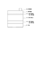
非晶質シリコン系薄膜を用いた薄膜光起電力素子は、一般的にはpin接合構造を有しており光電変換は主にi型半導体層で行われる。図1はpin型光起電力素子の一例を示す模式図である。基板101、n型半導体層(またはp型半導体層)102、i型半導体層103、p型半導体層(またはn型半導体層)104、透明電極105、および集電電極106等からこの光起電力素子は構成されている。
【0005】
接合特性を改善するためにp型半導体層やn型半導体層を微結晶する試みは、これまで数多くなされてきた。例えば、特開昭57−187971には、i型半導体層が非晶質シリコンからなり、p型半導体層及びn型半導体層のうち少なくとも光の入射する側にある層を平均粒径100Å以下の微結晶シリコンとすることにより出力電流及び出力電圧の向上を図る方法が開示されている。
【0006】
しかしながら、i型半導体層に非晶質シリコンをもちいたpin型太陽電池では、光照射時にi型半導体層の欠陥密度が増加し、光電変換率の低下を引き起こす現象(所謂Staebler−Wronski効果)が起こる場合があり、実用上、大きな問題となっていた。
【0007】
近年、非晶質シリコン系薄膜起電力素子の光電変換層にi型の微結晶シリコンを用いる試みがなされている。i型半導体層に微結晶シリコン膜を用いたpin型太陽電池は、光劣化を伴わないという大きな利点を有する。例えば、Neufchatel大のShahらのグループは、25th IEEE PV Specialists Conference,Washington,May 13−17,1996において、p型半導体層、i型半導体層、n型半導体層の全層に微結晶シリコンを用いて作製した光電変換効率7.7%の光劣化を伴わないpin型微結晶シリコン太陽電池を報告している。同グループが採用した微結晶シリコンi型半導体層の形成方法は、基本的には、従来の高周波プラズマCVD法によるものと同じだが、プラズマの形成周波数として、110MHzのVHF帯周波数を採用している。
【0008】
しかしながら、Neufchatel大のShahらのグループの報告によると、微結晶シリコンi型半導体層の堆積速度は1.2Å/sで、その厚さは3.6μmであった。簡単な計算によって、微結晶シリコンi型半導体層の形成には、8時間以上もの長時間を要することが分かる。変換効率が比較的高く、また、光劣化がないとはいえ、スループットは非常に小であり、結果的に低コスト化を図るのが困難となってしまう。
【0009】
微結晶シリコンをi型半導体層に用いたpin太陽電池の量産を現実的なものとするためには、微結晶シリコンi型半導体層の形成速度を飛躍的に向上させることが、必須であるといえる。しかし、概して、非晶質シリコンや微結晶シリコンの形成速度を単純に大きくすると、形成膜最表面での格子緩和が阻害され、形成膜の品質は低下する傾向があることが、これまでの多くの研究により明らかにされている。
【0010】
基体温度を上昇させることによって格子緩和を促進させることは可能であるが、この場合、i型半導体層に先立って形成したn型半導体層(あるいはp型半導体層)からのリン(あるいはボロン)といったドーパントの拡散が顕著となってi型半導体層の品質を損ない、結果的に作成した太陽電池の特性も低下させてしまうおそれがあった。高周波プラズマCVD法によって形成したi型微結晶シリコンは内因的に弱いn型であるといわれており、とりわけ、リンなどのn型ドーパントのi型微結晶シリコンへの拡散は抑制することが好ましい場合が多い。
【0011】
また、微結晶は非晶質シリコンに比べ光安定性に優れるため有望視されているが、従来のままでは欠陥が多いという問題点があった。
【0012】
【発明が解決しようとする課題】
そこで、本発明は、こうした問題を解決する光起電力素子、光電変換素子、及びそれらの製造方法を提供することを目的とする。
【0013】
即ち、本発明は、半導体層の形成速度を数〜数+Å/sと高速にしても、電気的、光学的特性に優れたi型非単結晶シリコン層の形成、特にi型微結晶シリコン層の形成が可能である素子及び方法を提供することを目的としている。
【0014】
また、本発明は、i型非単結晶シリコン層形成時間、特にi型微結晶シリコン層形成時間の短縮を図ることでn型半導体層あるいはp型半導体層からのリンやボロンといったドーパントの拡散による悪影響を抑制することを目的としている。
【0015】
さらに、本発明は、積層構造光起電力素子のi型半導体層に微結晶シリコンを適用し、短絡光電流、開放端電圧を改善しながら、光劣化を小さくして、光起電力素子の変換効率の向上、および生産性を高めることを目的としている。
【0016】
なお、本発明において、i型半導体層とは、実質的に真性な半導体層をいう。即ち、微量の不純物が混じることによって完全な真性半導体層でなくなってしまっているものも含む。
【0017】
【課題を解決するための手段】
そこで、本発明は、p型半導体層とi型半導体層とn型半導体層とが積層されたpin構造の半導体層を有する光起電力素子において、前記i型半導体層が非単結晶半導体からなり、該i型半導体層のX線回折法及びSherrerの式により求めた結晶粒の平均粒径分布が膜厚と垂直な面方向で不均一であることを特徴とする光起電力素子及び光電変換素子を提供する。
【0018】
また、本発明は、p型半導体層とi型半導体層とn型半導体層とが積層されたpin構造の半導体層を有する光起電力素子の製造方法において、前記i型半導体層を周波数50〜2450MHz、圧力0.001〜0.5Torr、投入電力密度0.001〜0.5W/cm3 の条件で高周波プラズマCVD法により形成することを特徴とする光電変換素子の製造方法及び光電変換素子の製造方法を提供する。
【0019】
特に、前記形成条件を成膜時に変化させることにより、i型半導体層内の結晶粒の平均粒径分布が膜厚と垂直な面方向で不均一とする製造方法を提供する。
【0020】
【発明の実施の形態】
以下、本発明の好適な実施態様について説明する。
【0021】
まず、本発明にかかる光起電力素子の構成の一例を図1を用いて説明する。この光起電力素子は、基板101、n型半導体層(又はp型半導体層)102、i型半導体層103、p型半導体層(又はn型半導体層)104、透明電極105、及び集電電極106から構成される。また、基板101上に金属層(裏面電極層)、透明導電層を順に設け、その上にn型半導体層(又はp型半導体層)102を設けた構成にしてもよい。
【0022】
以下、本発明の光起電力素子の各層について順に説明する。
【0023】
(基板)
基板101の材料としては、金属、樹脂、ガラス、セラミクス、半導体バルク等の導電性材料、絶縁性材料が必要に応じて用いられる。その表面は平滑であってもよいが、山の高さが0.1〜1.0μmの微細な凹凸を有していても良い。基板101として導電性基板などの不透明基板を用いる場合は、基板と反対側から光が入射するようにする。基板101として透明基板を用いて基板側から光が入射する構成としてもよい。
【0024】
基板101の形状としては、シート状、長尺状のシートを円筒状に巻き付けたロール状、あるいは円筒体等が望ましい。
【0025】
導電性材料としては、メッキ鋼板、NiCr、ステンレス、Al、Cr、Mo、Au、Nb、Ta、V、Ti、Pt、Pb、Sn等の金属又はこれらの合金が好適に用いられる。
【0026】
絶縁性材料としては、ポリエステル、ポリエチレン、ポリカーボネート、セルロースアセテート、ポリプロピレン、ポリ塩化ビニル、ポリ塩化ビニリデン、ポリスチレン、ポリアミド等の合成樹脂、又は、ガラス、セラミクス、紙等が挙げられる。
【0027】
基板101の厚さは適宜決定することができるが、光起電力素子を成型する上で柔軟性が要求される場合には薄くすることが出来る。但し、機械的強度を高めるために10μm以上とすることが好ましい。
【0028】
基板101の表面に凹凸を設ける(テクスチャー化する)には、例えば、化学エッチングまたは切削加工により鋭角を持ったジグザク状に基板表面を加工する。具体的には、化学研磨法、電解研磨法、等の化学的表面加工法、又はダイヤモンド、カーボランダム、アランダム、等の機械的研磨法により、凹凸を制御しながら基板表面を加工し、その後、エッチングすることにより多重凸面上の尖端をなくすといった方法をとることができる。
【0029】
また、基板を長尺の形状とすることによって連続成膜に対応させることができる。特に、ステンレス、ポリイミド等は可撓性を有するため長尺基板の材料として好適である。
【0030】
(裏面電極層)
裏面電極層は、半導体層から見て光の入射側でない側に設けられる電極層である。裏面電極層は、電極としての役割と、半導体層を透過してきた光を反射して半導体層で再利用させる反射層としての役割を有する。
【0031】
裏面電極層の材料としては、金、銀、銅、アルミニウム、ニッケル、鉄、クロム、モリブデン、タングステン、チタン、コバルト、タンタル、ニオブ、ジルコニウム等の金属、又はステンレス、AlSi等の合金、が好適に用いられる。特に、アルミニウム、銅、銀、金が反射率が高く好適である。裏面電極層は、蒸着、スパッタリング、めっき、水溶液からの電解析出、印刷等の方法で形成することができる。
【0032】
裏面電極層の厚さは10nm〜5000nmとすることが好ましい。
【0033】
裏面電極層の表面に凹凸を設けることにより、反射光の半導体層内での光路長を延ばし、素子の短絡電流(Jsc)を増大させることができる。
【0034】
裏面電極層は複数の層の積層構造としてもよい。また、基板101が導電性を有する場合には裏面電極層を形成しなくてもよい。但し、基板101が絶縁性である場合には、裏面電極層は必須となる。
【0035】
(透明導電層)
透明導電層は、裏面電極層と半導体層との間に設けられる層である。透明導電層は裏面電極層での乱反射を増大させる役割を有する。具体的には、透明導電層表面でのテクスチャー構造による乱反射と透明導電層での多重反射とによって光を光起電力素子内に閉じ込めて、半導体層内の光路長を延ばし、光起電力素子の短絡電流(Jsc)を増大させる。また、透明導電層は、裏面電極層の金属が半導体層へ拡散あるいはマイグレーションを起こし光起電力素子がシャントするのを防止する役割も有する。さらに、透明導電層に適度な抵抗を持たせることにより、半導体層のピンホール等の欠陥によるショートを防止する。透明導電層の導電率は10-8(1/Ωcm)以上10-1(1/Ωcm)以下であることが望ましい。また、透明導電層には高い透過率が要求される。650nm以上の光の透過率が80%以上であることが好ましく、85%であることがより好ましく、90%以上であることがさらに好ましい。
【0036】
透明導電層の層厚は用いられる材料の屈折率によって適宜好ましい膜厚に設定すればよく、例えば50nm〜10μmに設定することができる。
【0037】
透明導電層は、ZnO、ITO(インジウム錫酸化物)、In2 O3 、SnO2、TiO2 、CdO、Cd2 SnO4 、Bi2 O3 、MoO3 ,NaX WO3 等の導電性酸化物を蒸着、スパッタリング、電解析出、CVD、スプレー、スピンオン、ディッピング、メッキ等の方法を用いて成膜することにより形成することができる。これらの化合物に導電性を変化させる物質を含有させてもよい。透明導電層をテクスチャー化するには、例えば、スパッタリング法においては、該層の形成温度を200℃以上とすれば良い。また、いずれの形成方法においても、該層形成後に弱酸により表面をエッチングするのも、テクスチャー化の効果を高める点で有効である。
【0038】
(半導体層)
本発明に用いられる半導体層の材料としては、Si、C、Ge等のIV族元素を用いたもの、あるいはSiGe、SiC、SiSn等のIV族合金を用いたものが用いられる。
【0039】
また、以上の半導体材料の中で、本発明の光起電力装置に特に好適に用いられる半導体材料としては、a−Si:H(水素化非晶質シリコンの略記)、μc−Si:H(水素化微結晶シリコンの略記)、a−Si:F、μc−Si:F、a−Si:H:F、μc−Si:H:F、a−SiGe:H、μc−SiGe:H、a−SiGe:F、μc−SiGe:F、a−SiGe:H:F、μc−SiGe:H:F、a−SiC:H、μc−SiC:H、a−SiC:F、μc−SiC:F、a−SiC:H:F、μc−SiC:H:F等のIV族及びIV族合金系非単結晶半導体材料が挙げられる。
【0040】
また、半導体層は価電子制御及び禁制帯幅制御を行うことができる。具体的には半導体層を形成する際に価電子制御剤又は禁制帯幅制御剤となる元素を含む原料化合物を単独で、又は前記堆積膜形成用原料ガス又は前記希釈ガスに混合して成膜空間内に導入してやれば良い。
【0041】
また、半導体層は、価電子制御によって、少なくともその一部が、p型およびn型にドーピングされ、少なくとも一組のpin接合を形成する。そして、pin接合を複数積層することにより、いわゆるスタックセルの構成になる。
【0042】
因みに、特開昭62−209871には、p型半導体層またはn型半導体層に微結晶シリコンを用いた際にp/i或いはn/i界面の接合特性を改善するための方法として、p型半導体層或いはn型半導体層に向かって非晶質i半導体層の微結晶化の度合を順次大きくする方法が開示されている。しかし、同公報に記載の技術は、単に非晶質i型半導体層のp/i或いはn/i界面の結晶化の度合を高めるというものであり、i型半導体層の結晶粒径分布に関しては一切示唆がない。
【0043】
結晶粒径と結晶化の度合いとは全く異なる因子であり、一方を規定することによって他方が一義的に定まるものではない。
【0044】
結晶粒径の制御は後述するようにpin太陽電池における量子効果、多重反射効果、及び電流担体の拡散長の制御効果等、単に結晶化度を制御するのみでは得られない制御効果を有するものである。
【0045】
これに対して、結晶化の度合いとは単に結晶として存在する割合を示すに過ぎない。単に結晶化度を高くするだけでは、結晶粒径が非常に小さい場合、或いは必要以上に大きい場合、さらには例えば異常粒成長により極端に結晶粒径が大きなものとそれ以外のものとが混在した状態になる場合等がある。このような結晶化の度合いのみを制御した堆積膜を光起電力素子に用いた場合、ある程度の特性を得ることが出来るが、量子効果、多重反射効果、結晶中の電流担体の拡散長の制御効果等の効果を充分に発揮することができず、結晶粒径に起因する効果を光起電力素子に反映させることが困難になる。
【0046】
即ち前記公報記載の発明は、特に結晶粒径分布を特定の数値範囲内で不均一に制御するという本発明とは目的および効果も、全く異なる思想の発明である。
【0047】
また、特開昭63−58974には、p型半導体層を結晶質部分(p1)と非晶質部分(p2)の2つの部分で構成するとともに、結晶質部分(p1)を非晶質部分(p2)に向かって、その結晶質の割合を漸次減少させる方法が開示されている。しかし、同公報に記載の技術も前記公報に記載の技術と同様に、単に電極層であるp型半導体層の結晶質の割合を変化させる方法について述べたものであり、光電変換層領域を有するi型半導体層の結晶粒径分布に関しては一切の示唆がなく、特に結晶粒径分布を特定の数値範囲内で不均一にする制御するという本発明とは、目的および効果も、全く異なる思想の発明である。
【0048】
従来、pin型微結晶シリコン太陽電池のi型半導体層は図3−1あるいは図3−2のように、層内で均一な粒径分布をしていた。微結晶シリコンはその物理的メカニズムの詳細は不明な点が多いが、単結晶シリコンよりも観測される光吸収係数が大きい。これは、微結晶粒子のサイズに起因する量子効果(粒径を特定の大きさに制御することによって量子効果が得られ、大きな結晶よりも吸収係数が向上する)や、粒子間での光の多重反射(結晶粒界では光が反射しやすくなるため、この結晶粒界における反射面の大きさや結晶粒界の密度を結晶粒径を制御することによって調整する)などの効果によるものと考えられている。これらの効果を発揮させるためには、微結晶粒径は数百Å以下の小粒径が好ましい。しかしながら、一方で、素子性能を向上させるためには、電流担体の拡散長を増大させたいという要求もあり、この場合、微結晶粒径は大きいほど好ましい(1つの結晶中では電流担体は拡散し易いが、結晶粒界は逆に電流担体の拡散障壁となり易い)。従って、これまでのように、結晶粒径がi型半導体層の全域にわたって均一な分布をした構成では、前述の相反する2つの要求を同時に満足することができないという問題があった。本発明は、こうした問題を解決するために結晶粒界と光起電力素子の特性との相関を検討した上で、i型半導体層の各領域での結晶粒径を最適に制御することによって光起電力素子の特性を格段に向上させるものである。以下、それぞれの半導体層(特にi型半導体層)について詳細に述べる。
【0049】
本発明においては、前記i型半導体層内に存在する結晶粒の粒径分布を、膜厚方向及び/又は面方向で積極的に不均一とするものである。この場合、p/i、n/i界面近傍領域およびそれ以外の領域(i型半導体バルク領域)の結晶粒径の大小の組み合わせとして、例えば図3−3〜図3−9に示すような構成が考えられる。
【0050】
図3−3〜図3−5の場合(p,n界面近傍で粒径大)
p/i、n/i界面近傍領域での粒径を大とするとp型半導体層およびn型半導体層との接合特性が改善される。n型半導体層近傍の粒径を大とした図3−3では、n型半導体層からリン拡散を抑制する効果もある。また、p型半導体層近傍の粒径を大とした図3−4では、光入射側の接合が改善されるため、開放電圧や曲線因子の改善に著しい効果を発揮する。p型半導体層およびn型半導体層近傍の両方の粒径を大とした図3−5では、図3−3、図3−4で説明した両方の効果が得られ、さらに好ましいものである。図3−3〜図3−5ではi型半導体層内のp/i、n/i界面近傍以外の領域(i型半導体層バルク領域)の粒径が小さいので、光吸収が良好で光生成電流も大きくすることができる。粒径の変化は不連続であってもよいが、連続的であれば、i型半導体層の界面準位密度を低減させ、光生成キャリアの再結合を抑制できるので、非常に好ましい。
【0051】
図3−6〜図3−8の場合(p/i、n/i界面近傍で粒径小)
比較的粒径の大きい微結晶を高速で形成する場合に好適な構成である。i型半導体層バルク領域の結晶粒径が大きい場合、光生成キャリアの拡散長が著しく向上するので、曲線因子の非常に良好なpin太陽電池を得ることができる。ただし、粒径が大きくなるにつれて、i型半導体層バルクの特性は、単結晶シリコンの特性に近づいてくる。このため、太陽電池として十分な特性を発揮するには、膜厚を大きくする必要が生じてくる。本発明で用いられるp/i、n/i界面近傍での小粒径の微結晶は、光吸収の効率がよく、また、機械的な歪みも吸収できるという効果がある。このために、大粒径のi型半導体層バルクの膜厚を低減させることが可能であるとともに、p型半導体層あるいはn型半導体層との膨張係数の違い等に起因して発生する欠陥を抑制できるという利点がある。i型半導体層バルクの粒径よりもp型半導体層あるいはn型半導体層の粒径がかなり小さいとき、界面近傍での小粒径領域は接合面での粒径のミスマッチを緩和させる働きもある。小粒径領域は図3−6のようにn/i界面側にあっても、図3−7のようにp/i界面側にあっても、図3−8のようにp/i界面、n/i界面両側にあってもよい。粒径の変化は不連続であってもよいが、連続的であれば、i型半導体層の界面準位密度を低減させ、光生成キャリアの再結合を抑制できるので、非常に好ましい。
【0052】
図3−9の場合(層厚方向粒径大小の周期的繰り返し)
小粒径による光吸収増大効果および歪みの吸収の効果、大粒径による拡散長増大の効果の相乗効果を期待できる。小粒径と大粒径でのバンドギャップの違いを利用して量子井戸を形成することにより、光生成キャリアの移動度をも向上させることができ、曲線因子をさらに向上できる。粒径の変化は不連続であってもよいが、連続的であれば、i型半導体層の界面準位密度を低減させ、光生成キャリアの再結合を抑制できるので、非常に好ましい。
【0053】
図3−10の場合(面方向粒径不均一)
本発明では、図3−10のように、面方向に粒径が不均一となっているのも好ましい例として挙げられる。この場合も、小粒径による光吸収増大効果および歪みの吸収の効果、大粒径による拡散長増大の効果の相乗効果を期待できる。粒径の変化は不連続であってもよいが、連続的であれば、i型半導体層の界面準位密度を低減させ、光生成キャリアの再結合を抑制できるので、非常に好ましい。
【0054】
図3−11の場合(面方向粒径大小の周期的繰り返し)
太陽電池などの光起電力素子をモジュール化する場合には、集電電極が規則的に配置されている。集電電極下の粒径が大となるように面方向大小大繰り返しを周期的に行うことは光生成キャリアの収集の効率を向上させることができ、好都合である。この例でも、粒径の変化は不連続であってもよいが、連続的であれば、i型半導体層の界面準位密度を低減させ、光生成キャリアの再結合を抑制できるので、非常に好ましい。
【0055】
以上述べたことに関して、前記i型半導体層内の最大平均粒径領域の水素含有量が、それ以外の前記i型半導体層内の領域の水素含有量よりも小さいことが好ましい。とりわけ、前記i型半導体層内の最大平均粒径領域の水素含有量が、10%以下で、それ以外の前記i型半導体層内の領域の水素含有量が3〜20%の範囲にあれば、なお好ましい。さらに、前記i型半導体層内の最大平均粒径に対する最小平均粒径の比が0.9以下であることが好ましい。さらに、前記非単結晶シリコンは最小平均粒径が20Å〜1μmの微結晶シリコン、最大平均粒径が50Å〜10mmの微結晶シリコンあるいは多結晶シリコンにより構成されていることが好ましい。さらに、n/i界面近傍でi型半導体層内のドーパント濃度が2×1017cm-3以下(実質的にノンドープ)となっていることが好ましい。さらに、n型半導体層及び/又はp型半導体層が微結晶シリコンを有することが好ましい。さらに、n型半導体層及び/又はp型半導体層と前記i型半導体層の界面にi型の非晶質シリコン界面層を有することが好ましい。さらに、前記非単結晶シリコンは、周波数が50〜2450MHzの範囲、形成圧力が0.001〜0.5Torrの範囲、投入電力密度が0.001〜0.5w/cm3 の範囲において、高周波プラズマCVD法により形成圧力されることことが好ましい。
【0056】
また、これらの粒径、水素量などの抑制は、目的とする太陽電池の特性あるいは生産性などを考慮して適宜選択することにより、本発明の効果を一層高めることが可能となる。
【0057】
例えば、より高い開放電圧の太陽電池が必要とされる場合には、本発明の範囲内で水素量を多くすることが好ましい。また、光安定性が特に必要とされる太陽電池を得るには、本発明の範囲内で水素量を少なくすることが好ましい。さらに、i型半導体層の形成速度を増大させることにより、生産性の飛躍的な向上を図るには、本発明の範囲内で、より高い周波数や、より大きな投入電力密度や、より低い周波数を選ぶことが好ましい。
【0058】
(ドーピング層(n型半導体層,p型半導体層))
ドーピング層の母材は非晶質シリコン系あるいは微結晶シリコン系半導体から構成される。非晶質(a−と略記する)シリコン系半導体としては、a−Si、a−SiC、a−SiO、a−SiN、a−SiCO、a−SiON、a−SiNC、a−SiCON等が挙げられる。母材は微結晶シリコンを含有した非晶質シリコン系半導体であってもよい。伝導型をp型またはn型にするために導入される価電子制御剤の導入量は、1000ppm〜10%が好ましい範囲として挙げられる。水素(H、D)及びフッ素は未結合手を補償する働きをし、ドーピング効率を向上させるものである。水素及びフッ素含有量は0.1〜30atom%が最適値として挙げられる。特にドーピング層が微結晶シリコンを含有する場合、0.01〜10atom%が最適量として挙げられる。炭素、酸素、窒素原子の導入量は0.1ppm〜20%、微量に含有させる場合には、0.1ppm〜1%が好適な範囲である。また、電気特性としては活性化エネルギーが0.2eV以下のものが好ましく、比抵抗としては100Ωcm以下のものが好ましく、1Ωcm以下が最適である。
【0059】
(i型半導体層)
本発明の光起電力素子において、i型半導体層は光励起キャリアを発生、輸送する最も重要な層である。本発明で用いられる非単結晶シリコンは、好ましくは13.56MHz乃至2.45GHzの範囲にある高周波プラズマCVD法によって形成されるもので、吸光係数の光子エネルギー依存性が、高エネルギー側で非晶質シリコンに近く、低エネルギー側で結晶シリコンに近いものである。本発明は、i型半導体層内に存在する結晶粒の粒径分布を不均一とすることによって、pin太陽電池の特性を向上させようとするものであり、例えば、前述の図3−3〜図3−11に示すような構成が、好ましい具体例として挙げられる。
【0060】
(透明電極)
透明電極105は、その膜厚を適当に設定することにより反射防止膜の役割をかねることが出来る。
【0061】
透明電極はITO(インジウム錫酸化物)、ZnO、In2 O3 、SnO2 等の材料を、蒸着、CVD、スプレー、スピンオン、浸漬等の方法を用いて成膜することにより形成することができる。これらの化合物に導電率を変化させる物質を含有させてもよい。
【0062】
かかる物質としては、透明電極がZnOの場合には、Al、In、B、Ga、Si、F等が好適に用いられ、透明電極がIn2 O3 の場合には、Sn、F、Te、Ti、Sb、Pb等が好適に用いられ、透明電極がSnO2 の場合には、F、Sb、P、As、In、Tl、Te、W、Cl、Br、I等が好適に用いられる。
【0063】
透明電極の透過率は550nmにおいて80%以上であることが好ましく、85%以上であることがより好ましい。また、透明電極の抵抗率は5×10⁻³Ωcm以下であることが好ましく、1×10⁻³Ωcm以下であることがより好ましい。
【0064】
(集電電極)
集電電極106は集電効率を向上させるために設けられる。その形成方法として、マスクを用いてスパッタによって電極パターンの金属を形成する方法や、導電性ペーストあるいは半田ペーストを印刷する方法、金属線を導電性ペーストで固着する方法などがある。
【0065】
なお、必要に応じて光起電力素子の両面に保護層を形成することがある。同時に鋼板等の補強材を併用してもよい。
【0066】
なお、以上ではpin構造の光起電力素子について説明したが、pinpin構造やpinpinpin構造などのpin構造を積層した光起電力素子、あるいはnip構造や、nipnip構造、nipnipnip構造といったnip構造を積層した光起電力素子についても本発明は適用できるものである。
【0067】
また、以上では光起電力素子について述べたが、光電変換素子についても同様の構成とすることができる。
【0068】
【実施例】
以下、本発明の光起電力素子の作製例を挙げて詳細に説明するが、本発明はこれによって何ら限定されるものではない。
【0069】
以下の実施例では半導体薄膜の形成装置としてを図2に示す装置を用いた。基板201は、形成装置内壁上部に保持され、ヒータ202により所望の温度となるよう加熱されている。原料ガスはガス導入管209及びバルブ210を通して装置内部へと導入される。原料ガスはいずれも超高純度に精製されたもので、SiH4 ガス、PH3 /H2 (希釈度:2%)ガス、B2 H6 /H2 (希釈度:2%)ガス、およびH2 ガスを用いた。プラズマの発生源としては、マイクロ波、VHF、RFの各周波数帯の電源を、必要に応じて、それぞれ単独で、あるいは、複数組み合わせて使用した。実質的な放電空間容積は約3000cm3 である。原料ガス導入に先立って、装置内部をターボ分子ポンプをもちいて10-5Torr程度まで排気した。
【0070】
〈予備実験1〉光起電力素子の作製に先立ち、ノンドープの微結晶シリコンの単層膜を形成し形成膜の評価を行った。基板として、厚さ0.5mmのステンレス板に0.5μmのZnOをスパッタ法により堆積したものを用いた。基板上に、表1に示す条件(小粒径微結晶・高速堆積条件)でi型微結晶シリコン膜を約2μm堆積した。
【0071】
【表1】

〈評価1〉ラマン散乱法、X線回折法、反射赤外吸収法をもちいて〈予備実験1〉で形成した微結晶シリコン膜の評価を行った。ラマン散乱のラマンシフトでは図4に示すように微結晶シリコンに対応する波数520cm-1付近の鋭いピークが見られた。次に、X線回折による評価(図5)から、Scherrerの式:t=0.9λ/Bcosθ(t:粒径、B:半値幅、θ:ブラッグ角)を用いて結晶粒径の見積もりを行った。見積もられた粒径は(111)面の場合約150Åであった。回折ピークはややブロードであり、形成膜は微結晶シリコンと非晶質シリコンの混晶である考えられる。反射赤外吸収法による波数2100cm-1付近の赤外吸収スペクトルより算出した含有水素量は約6%であった。
【0073】
〈予備実験2〉前記〈予備実験1〉と同様の基板を用い、表2に示す条件(大粒径微結晶・低速堆積条件)で微結晶シリコン膜を約2μm堆積した。
【0074】
【表2】
〈評価2〉ラマン散乱法、X線回折法をもちいて〈予備実験2〉で形成した微結晶シリコン膜の評価を行った。ラマン散乱のラマンシフトでは微結晶シリコンに対応する波数520cm-1付近の鋭いピークが見られた。次に、X線回折による評価から、Sherrerの式:t=0.9λ/Bcosθ(t:粒径、B:半値幅、θ:ブラッグ角)を用いて結晶粒径の見積もりを行った。見積もられた粒径は(111)面の場合、約200Åであった。回折ピークは、幾分ブロードであり、形成膜は微結晶シリコンと非晶質シリコンの混晶であると考えられるが、前記〈予備実験1〉の形成膜よりも結晶性は良好であると考えられる。反射赤外吸収法による波数2100cm-1付近の赤外吸収スペクトルより算出した含有水素量は約4%であった。
【0076】
〈実験例1〉次に、図2に示す形成装置を用いて図1の構成をした太陽電池を作製した例について説明する。
【0077】
まず、基板の作製を行った。厚さ0.5mm、50×50mm2 のステンレス板をアセトンとイソプロピルアルコールに浸漬して超音波洗浄を行った後、温風乾燥させた。DCマグネトロンスパッタ法を用い、形成温度300℃でテクスチャリング構造を有する膜厚0.8μmのAgを堆積させ、続いて形成温度300℃でテクスチャリング構造を有する膜厚4.0μmのZnOの透明導電膜を堆積した。
【0078】
次に、堆積装置を用いてZnO透明導電膜上にpin接合を形成した。n型半導体層は、不図示の形成装置をもちい、表3の条件でRF法により約200Å堆積した。i型半導体層は、図2の形成装置を用い、表1の条件(粒径小)で、VHF(105MHzの高周波)とRF(13.56MHzの高周波)を重畳して、約1.0μm堆積した。p型半導体層は、不図示の形成装置をもちい、表4の条件でRF法により約100Å堆積した。
【0079】
【表3】
【表4】
続いて、透明電極として、ITOをITOターゲットを用いたスパッタリング法により、約600Å堆積した。さらに、集電電極として、Auを電子ビームを用いた真空蒸着法により約8000Å堆積した。
【0082】
このpin型太陽電池を(セル−1)と呼ぶ(図3−1に相当)。
【0083】
〈実験例2〉本例では、i型半導体層を表2の条件(粒径大)で約1.0μm堆積した。i型半導体層以外は、前記〈実験例1〉と同条件で太陽電池を作製した。
【0084】
この太陽電池を(セル−2)と呼ぶ(図3−2に相当)。
【0085】
〈実験例3〉i型半導体層以外は前記〈実験例1〉と同条件で太陽電池を作製した。本例では、n型半導体層近傍のi型半導体層を表2(粒径大)に示す条件で約1000Å堆積し、続けて、n型半導体層近傍以外のi型半導体層を表1に示す条件(粒径小)で約9000Å堆積した。
【0086】
この太陽電池を(セル−3)を呼ぶ(図3−3に相当)。
【0087】
〈実験例4〉i型半導体層以外は前記〈実験例1〉と同条件で太陽電池を作製した。本例では、n型半導体層上に、まず、表1に示す条件(粒径小)でi型層を約9000Å堆積し、続けて、p型半導体層近傍のi型半導体層を表2に示す条件(粒径大)で約1000Å堆積した。
【0088】
この太陽電池を(セル−4)と呼ぶ(図3−4に相当)。
【0089】
〈実験例5〉i型半導体層以外は前記〈実験例1〉と同条件で太陽電池を作製した。本例では、n型半導体層上に、まず、表2に示す条件(粒径大)でi型半導体層を約1000Å堆積し、続けて、表1に示す条件(粒径小)でi型半導体層を約8000Å堆積し、更に、p型半導体層近傍のi型半導体層を表2に示す条件(粒径大)で約1000Å堆積した。
【0090】
この太陽電池を(セル−5)と呼ぶ(図3−5に相当)。
【0091】
〈実験例6〉i型半導体層以外は前記〈実験例1〉と同条件で太陽電池を作製した。本例では、n型半導体層近傍のi型半導体層を表1に示す条件(粒径小)で約1000Å堆積し、続けて、n型半導体層近傍以外のi型半導体層を表2に示す条件(粒径大)で約9000Å堆積した。
【0092】
この太陽電池を(セル−6)と呼ぶ(図3−6に相当)。
【0093】
〈実験例7〉i型半導体層以外は前記〈実験例1〉と同条件で太陽電池を作製した。本例では、n型半導体層上に、まず、表2に示す条件(粒径大)でi型半導体層を約9000Å堆積し、続けて、p型半導体層近傍のi型半導体層を表1に示す条件(粒径小)で約1000Å堆積した。
【0094】
この太陽電池を(セル−7)と呼ぶ(図3−7に相当)。
【0095】
〈実験例8〉i型半導体層以外は前記〈実験例1〉と同条件で太陽電池を作製した。本例では、n型半導体層上に、まず、表1に示す条件(粒径小)でi型半導体層を約1000Å堆積し、続けて、表2に示す条件(粒径大)でi型半導体層を約8000Å堆積し、更に、p型半導体層近傍のi型半導体層を表1に示す条件(粒径小)で約1000Å堆積した。
【0096】
この太陽電池を(セル−8)と呼ぶ(図3−8に相当)。
【0097】
〈実験例9〉i型半導体層以外は前記〈実験例1〉およびと同条件で太陽電池を作製した。本例では、表1に示す条件(粒径小)でのi型半導体層上に表2に示す条件(粒径大)でi型半導体層を堆積したものを1周期とし、n型半導体層上に20周期堆積した。
【0098】
この太陽電池を(セル−9)と呼ぶ(図3−9に相当)。
【0099】
〈実験例10〉i型半導体層以外は前記〈実験例1〉と同条件で太陽電池を作製した。本例では、n型半導体層形成後、n型半導体層のマスキングを行い、表1に示す条件(粒径小)で膜厚10000Åのi型半導体層を面方向に5mm間隔で形成した。続けて、別のマスキングを行い、前記表1に示す条件のi型半導体層の間を埋めるように、表2の条件(粒径大)で膜厚10000Åのi型半導体層を形成した。
【0100】
この太陽電池を(セル−10)と呼ぶ(図3−10に相当)。
【0101】
〈実験例11〉i型半導体層以外は前記〈実験例1〉と同条件で太陽電池を作製した。本例では、受光部分は表1の条件で形成、金属電極の下部のみを表2の条件(粒径大)で形成した。金属電極の間隔は10mmであり、i型半導体層は面方向に周期的に、表1の条件(粒径小)と表2の条件(粒径大)が繰り返されて形成されている。
【0102】
この太陽電池を(セル−11)と呼ぶ(図3−11に相当)。
【0103】
開放電圧Voc、短絡電流密度Jsc、曲線因子FF、変換効率η、光安定性S(1 SUN 500時間照射後の変換効率の低下率)について、(セル−2)を基準として比較して示すと表5のようになった。
【0104】
【表5】
p、n界面近傍にi型半導体層バルク領域よりも大きな粒径を用いた(セル−3)〜(セル−5)では、(セル−1)に比べてVoc、FFが改善され、セルのηを向上させることができた。また、光安定性Sも改善が見られた。逆に、p、n界面近傍にi型半導体バルク領域よりも小さな粒径を用いた(セル−6)〜(セル−8)では、(セル−2)に比べてJsc、FFが改善され、セルのηを向上させることができた。この例では、小粒径領域の膜厚が十分小さいため、光安定性はほとんど低下しなかった。さらに、層厚方向に周期的に粒径を変化させた(セル−9)では、FFの向上が大きく、セルのηを大幅に向上させることができた。
【0106】
また、面方向に不均一な粒径分布をもつ(セル−10)でも、Jscが改善され、ηを向上させることができた。また、金属電極の真下が大きな粒径となるように、面方向に周期的な粒径分布をもつ(セル−11)でも同様の効果が確認できた。
【0107】
〈実験例12〉〈実験例5〉の場合について、表1および表2の条件を基本に、粒径は変化させず、含有水素量を変化させた。その結果を表6に示す。表6に示すように、表2の条件(粒径大)の含有水素量が表1の条件(粒径小)の含有水素量よりも、小さいときに良好なセル特性が得られた。特に、表2の条件(粒径大)の含有水素量CH が10%以下で、表1の条件(粒径小)の含有水素量CH が3〜20%の範囲で良好なセル特性が得られた。これは、〈実験例5〉に限られるものではなく、前述の各実験例でも同様であった。
【0108】
【表6】
〈実験例13〉〈実験例5〉の場合について、表1および表2の条件を変化させて、それぞれの粒径を変化させた。ただし、表2の条件(粒径大)の粒径が表1の条件(粒径小)の粒径より常に大となるよう条件とした。表2の条件(粒径大)の粒径に対する、表1の条件(粒径小)の粒径に比を変化させて、セル特性の変化を調べた。その結果、表7に示すように、大粒径に対する小粒径の比が0.9以下の範囲で良好なセル特性が得られた。
【0110】
【表7】
〈実験例14〉図3−5の構成のpin型太陽電池について、粒径を広範囲に変化させて、特性の変化を調べた。その結果、表8に示すように、最小平均粒径が20Å〜1μmの微結晶であり、かつ、最大平均粒径が50Å〜10mmの微結晶あるいは多結晶で良好な特性が得られた。
【0112】
【表8】
〈実験例15〉図3−5の構成のpin型太陽電池について、n型半導体層内のドープ量を制御することによって、i型半導体層内のn/i界面近傍領域でのドーパント(リン)濃度を制御した。i型半導体層内のn/i界面近傍領域でのドーパント(リン)濃度は、i型半導体層およびp型半導体層形成後にSIMSにより測定した。その結果、表9に示すように、i型半導体層内のn/i界面近傍領域でのドーパント(リン)濃度が2×1017cm-3以下で良好なセル特性が得られた。
【0114】
【表9】
〈実験例16〉 図3−5の構成のpin型大型太陽電池について、n型半導体層及び/又はp型半導体層を微結晶シリコンで形成した。その結果、表10に示すように、従来の非晶質のn型半導体層及び/又はp型半導体層を用いた場合より、曲線因子が大幅に向上し、pinセルの特性も向上できた。
【0116】
【表10】
〈実験例17〉図3−5の構成のpin型太陽電池について、p/i界面及び/又n/i界面にi型の非晶質シリコンを100Å挿入した場合について調べた。その結果、表11に示すように、p/i界面及び/又n/i界面にi型の非晶質シリコンを挿入することで開放電圧および曲線因子が大幅に向上し、pinセルの特性も向上できた。
【0118】
【表11】
〈実験例18〉 本発明の光起電力素子に用いられる非単結晶シリコンを高周波プラズマCVD法により好適に形成できる形成条件の範囲を調べた。その結果、周波数が50〜2450MHzの範囲、形成圧力が0.001〜0.5torrの範囲、投入電力密度が0.001〜0.5w/cm3 の範囲にあることがわかった。周波数に関しては、上記の条件範囲内で高い周波数を使うと膜形成速度向上が容易となることが判明した。また、上記の条件範囲内で低い周波数を使うと放電維持が容易となり、セル特性の向上や歩留まり向上の点で有利であることが判明した。また、速度向上が容易であり、低コストの点で有利であることが判明した。また、形成圧力に関しては、用いる周波数に応じて最適範囲が異なるが、上記の条件範囲内でより低い圧力を用いると形成膜の微結晶化を促進できる傾向があることが判明した。また、投入電力密度に関しては、上記の条件範囲内でより大きい投入電力密度を用いると膜形成速度が向上できる効果があるが、前記、周波数や形成圧力を適当に選択することで、高速形成条件下においても、優れた品質も微結晶膜を選られる効果のあることが判明した。即ち、前記周波数範囲、形成圧力範囲、投入電力密度範囲は、本発明に好適な高品質の微結晶シリコン膜を、低コストで形成するのに極めて好適なものであることが判明した。
【0120】
【発明の効果】
以上説明したように、本発明によれば、光電変換効率および光安定性の優れた光起電力素子及び光電変換素子を高速かつ低コストで作製できる。また、本発明の光起電力素子は、高周波プラズマCVD法を用いて作製されるため、大面積化も容易で量産性も優れている。
【図面の簡単な説明】
【図1】光起電力素子の一例を示す模式的な概略断面図。
【図2】本発明の光起電力素子の製造に用いられる装置の一例を示す模式的な概略断面図。
【図3】本発明の光起電力素子のi型半導体層中の粒径分布の例を示す模式図。
【図4】予備実験1の素子のラマンシフトを示す図。
【図5】予備実験1の素子のX線回折結果を示す図。
【符号の説明】
101 基板
102 n型半導体層(p型半導体層)
103 i型半導体層
104 p型半導体層(n型半導体層)
105 透明電極
106 集電電極
201 基板
202 ヒーター
203 マイクロ波電源
204 マイクロ波導入窓
205 VHF電源
206 VHF電極
207 RF電源
208 RF電極
209 ガス導入管
210 バルブ[0001]
BACKGROUND OF THE INVENTION
The present invention relates to a pin-type photovoltaic element, a photoelectric conversion element, and a method for manufacturing the same, which include non-single-crystal silicon such as amorphous silicon, microcrystalline silicon, and polycrystalline silicon.
[0002]
[Prior art]
Conventionally, a high frequency (RF) typified by 13.56 MHz has been used for producing photovoltaic elements such as pin-type solar cells using amorphous silicon-based films and the like, and photoelectric conversion elements such as optical sensors. The plasma CVD method is widely known. However, in the plasma CVD method using a high frequency of 13.56 MHz, it has been confirmed that the quality of the formed film rapidly decreases as the thin film formation speed increases, and it is difficult to improve the throughput in mass production. there were.
[0003]
Therefore, a plasma CVD method using a microwave (MW) typified by 2.45 GHz is known as being capable of forming a relatively good quality thin film even if the thin film formation rate is relatively high. For example, as an example of forming an i-type semiconductor layer by microwave plasma CVD, "a-Si solar cell by microwave plasma CVD" Towafumi, Takeshi Watanabe, Juichi Shimada Proceedings of the 50th JSAP . 566 etc. are mentioned.
[0004]
A thin film photovoltaic element using an amorphous silicon thin film generally has a pin junction structure, and photoelectric conversion is mainly performed in an i-type semiconductor layer. FIG. 1 is a schematic diagram showing an example of a pin type photovoltaic device. The photovoltaic power from the substrate 101, the n-type semiconductor layer (or p-type semiconductor layer) 102, the i-type semiconductor layer 103, the p-type semiconductor layer (or n-type semiconductor layer) 104, the transparent electrode 105, the collecting electrode 106, and the like. The element is constructed.
[0005]
There have been many attempts to crystallize a p-type semiconductor layer and an n-type semiconductor layer in order to improve the junction characteristics. For example, in Japanese Patent Laid-Open No. 57-187971, an i-type semiconductor layer is made of amorphous silicon, and at least a layer on the light incident side of a p-type semiconductor layer and an n-type semiconductor layer has an average particle size of 100 mm or less. A method for improving output current and output voltage by using microcrystalline silicon is disclosed.
[0006]
However, in a pin-type solar cell using amorphous silicon for the i-type semiconductor layer, a phenomenon (so-called Staebler-Wronski effect) that the defect density of the i-type semiconductor layer increases during light irradiation and causes a decrease in the photoelectric conversion rate occurs. It may occur and has become a big problem in practical use.
[0007]
In recent years, attempts have been made to use i-type microcrystalline silicon for a photoelectric conversion layer of an amorphous silicon thin film photovoltaic device. A pin-type solar cell using a microcrystalline silicon film as an i-type semiconductor layer has a great advantage that it is not accompanied by light degradation. For example, the group of Shah et al. At Neufatel uses microcrystalline silicon for all layers of the p-type semiconductor layer, the i-type semiconductor layer, and the n-type semiconductor layer in 25th IEEE PV Specialists Conference, Washington, May 13-17, 1996. A pin-type microcrystalline silicon solar cell without photodegradation having a photoelectric conversion efficiency of 7.7% is reported. The method of forming the microcrystalline silicon i-type semiconductor layer adopted by the group is basically the same as that of the conventional high-frequency plasma CVD method, but adopts a VHF band frequency of 110 MHz as the plasma formation frequency. .
[0008]
However, according to a report of the group of Shah et al. At Neufatel University, the deposition rate of the microcrystalline silicon i-type semiconductor layer was 1.2 Å / s and its thickness was 3.6 μm. Simple calculation shows that it takes a long time of 8 hours or more to form the microcrystalline silicon i-type semiconductor layer. Although the conversion efficiency is relatively high and there is no light degradation, the throughput is very small, and as a result, it is difficult to reduce the cost.
[0009]
In order to make mass production of pin solar cells using microcrystalline silicon as an i-type semiconductor layer realistic, it is essential to dramatically increase the formation rate of the microcrystalline silicon i-type semiconductor layer. I can say that. However, in general, when the formation rate of amorphous silicon or microcrystalline silicon is simply increased, lattice relaxation at the outermost surface of the formed film is hindered, and the quality of the formed film tends to deteriorate. It has been clarified by research.
[0010]
Although it is possible to promote lattice relaxation by raising the substrate temperature, in this case, phosphorus (or boron) from an n-type semiconductor layer (or p-type semiconductor layer) formed prior to the i-type semiconductor layer, etc. There is a possibility that the diffusion of the dopant becomes conspicuous and the quality of the i-type semiconductor layer is impaired, and as a result, the characteristics of the produced solar cell are also deteriorated. It is said that i-type microcrystalline silicon formed by a high-frequency plasma CVD method is intrinsically weak n-type. In particular, it is preferable to suppress diffusion of n-type dopants such as phosphorus into i-type microcrystalline silicon. There are many.
[0011]
In addition, microcrystals are considered promising because they are superior in light stability compared to amorphous silicon.
[0012]
[Problems to be solved by the invention]
Then, an object of this invention is to provide the photovoltaic element, photoelectric conversion element, and those manufacturing methods which solve such a problem.
[0013]
That is, the present invention provides an i-type non-single-crystal silicon layer having excellent electrical and optical characteristics, particularly an i-type microcrystalline silicon layer, even if the semiconductor layer is formed at a high speed of several to several + Å / s. It is an object of the present invention to provide an element and a method capable of forming the structure.
[0014]
Further, the present invention is based on diffusion of dopants such as phosphorus and boron from an n-type semiconductor layer or a p-type semiconductor layer by shortening an i-type non-single crystal silicon layer formation time, particularly an i-type microcrystalline silicon layer formation time. The purpose is to suppress adverse effects.
[0015]
Furthermore, the present invention applies a microcrystalline silicon to the i-type semiconductor layer of the stacked structure photovoltaic device to improve the short-circuit photocurrent and open-circuit voltage while reducing the photodegradation and converting the photovoltaic device. It aims to improve efficiency and increase productivity.
[0016]
In the present invention, the i-type semiconductor layer refers to a substantially intrinsic semiconductor layer. In other words, it includes a layer that is not a complete intrinsic semiconductor layer due to a small amount of impurities.
[0017]
[Means for Solving the Problems]
Accordingly, the present invention provides a photovoltaic element having a pin structure semiconductor layer in which a p-type semiconductor layer, an i-type semiconductor layer, and an n-type semiconductor layer are stacked, wherein the i-type semiconductor layer is made of a non-single-crystal semiconductor. The i-type semiconductor layer Obtained by X-ray diffraction method and Serrer's formula Provided is a photovoltaic element and a photoelectric conversion element characterized in that the average grain size distribution of crystal grains is not uniform in a plane direction perpendicular to the film thickness.
[0018]
According to the present invention, in the method of manufacturing a photovoltaic device having a pin structure semiconductor layer in which a p-type semiconductor layer, an i-type semiconductor layer, and an n-type semiconductor layer are stacked, the i-type semiconductor layer is formed at a frequency of 50 to 50. 2450 MHz, pressure 0.001-0.5 Torr, input power density 0.001-0.5 W / cm Three A method for manufacturing a photoelectric conversion element and a method for manufacturing a photoelectric conversion element are provided, which are formed by a high-frequency plasma CVD method under the above conditions.
[0019]
In particular, the average particle size distribution of crystal grains in the i-type semiconductor layer can be obtained by changing the formation conditions during film formation. In the direction perpendicular to the film thickness A non-uniform manufacturing method is provided.
[0020]
DETAILED DESCRIPTION OF THE INVENTION
Hereinafter, preferred embodiments of the present invention will be described.
[0021]
First, an example of the configuration of the photovoltaic element according to the present invention will be described with reference to FIG. The photovoltaic element includes a substrate 101, an n-type semiconductor layer (or p-type semiconductor layer) 102, an i-type semiconductor layer 103, a p-type semiconductor layer (or n-type semiconductor layer) 104, a transparent electrode 105, and a collecting electrode. 106. Alternatively, a metal layer (back electrode layer) and a transparent conductive layer may be sequentially provided on the substrate 101, and an n-type semiconductor layer (or p-type semiconductor layer) 102 may be provided thereon.
[0022]
Hereinafter, each layer of the photovoltaic device of the present invention will be described in order.
[0023]
(substrate)
As a material of the substrate 101, a conductive material such as metal, resin, glass, ceramics, or semiconductor bulk, or an insulating material is used as necessary. The surface may be smooth, but may have fine irregularities with a peak height of 0.1 to 1.0 μm. When an opaque substrate such as a conductive substrate is used as the substrate 101, light is incident from the opposite side of the substrate. A transparent substrate may be used as the substrate 101 and light may be incident from the substrate side.
[0024]
As the shape of the substrate 101, a sheet shape, a roll shape obtained by winding a long sheet into a cylindrical shape, or a cylindrical body is desirable.
[0025]
As the conductive material, a plated steel plate, NiCr, stainless steel, Al, Cr, Mo, Au, Nb, Ta, V, Ti, Pt, Pb, Sn, or a metal such as these or an alloy thereof is preferably used.
[0026]
Examples of the insulating material include polyester, polyethylene, polycarbonate, cellulose acetate, polypropylene, polyvinyl chloride, polyvinylidene chloride, polystyrene, polyamide, and other synthetic resins, glass, ceramics, paper, and the like.
[0027]
The thickness of the substrate 101 can be determined as appropriate, but can be reduced when flexibility is required in molding the photovoltaic element. However, it is preferably 10 μm or more in order to increase the mechanical strength.
[0028]
In order to provide unevenness (texturization) on the surface of the substrate 101, for example, the substrate surface is processed in a zigzag shape having an acute angle by chemical etching or cutting. Specifically, the substrate surface is processed while controlling the unevenness by a chemical surface processing method such as a chemical polishing method, an electrolytic polishing method, or a mechanical polishing method such as diamond, carborundum, alundum, etc. Then, it is possible to take a method of eliminating the point on the multiple convex surface by etching.
[0029]
Further, by forming the substrate in a long shape, it is possible to cope with continuous film formation. In particular, stainless steel, polyimide, and the like are suitable as materials for long substrates because of their flexibility.
[0030]
(Back electrode layer)
The back electrode layer is an electrode layer provided on a side that is not the light incident side when viewed from the semiconductor layer. The back electrode layer has a role as an electrode and a reflection layer that reflects light transmitted through the semiconductor layer and reuses it in the semiconductor layer.
[0031]
As a material for the back electrode layer, gold, silver, copper, aluminum, nickel, iron, chromium, molybdenum, tungsten, titanium, cobalt, tantalum, niobium, zirconium, or other metals, or stainless steel, AlSi, or other alloys are suitable. Used. In particular, aluminum, copper, silver, and gold are preferable because of their high reflectance. The back electrode layer can be formed by a method such as vapor deposition, sputtering, plating, electrolytic deposition from an aqueous solution, or printing.
[0032]
The thickness of the back electrode layer is preferably 10 nm to 5000 nm.
[0033]
By providing irregularities on the surface of the back electrode layer, the optical path length of the reflected light in the semiconductor layer can be extended, and the short circuit current (Jsc) of the element can be increased.
[0034]
The back electrode layer may have a laminated structure of a plurality of layers. Further, when the substrate 101 has conductivity, the back electrode layer may not be formed. However, when the substrate 101 is insulative, the back electrode layer is essential.
[0035]
(Transparent conductive layer)
The transparent conductive layer is a layer provided between the back electrode layer and the semiconductor layer. The transparent conductive layer has a role of increasing irregular reflection at the back electrode layer. Specifically, light is confined in the photovoltaic element by irregular reflection due to the texture structure on the surface of the transparent conductive layer and multiple reflection at the transparent conductive layer, thereby extending the optical path length in the semiconductor layer, and Increase the short circuit current (Jsc). The transparent conductive layer also has a role of preventing the photovoltaic element from shunting due to diffusion or migration of the metal of the back electrode layer to the semiconductor layer. Furthermore, by giving an appropriate resistance to the transparent conductive layer, a short circuit due to a defect such as a pinhole in the semiconductor layer is prevented. The conductivity of the transparent conductive layer is 10 -8 (1 / Ωcm) or more 10 -1 It is desirable that it is (1 / Ωcm) or less. Further, the transparent conductive layer is required to have a high transmittance. The transmittance of light of 650 nm or more is preferably 80% or more, more preferably 85%, and further preferably 90% or more.
[0036]
What is necessary is just to set the layer thickness of a transparent conductive layer to a suitable film thickness suitably with the refractive index of the material to be used, for example, it can set to 50 nm-10 micrometers.
[0037]
The transparent conductive layer is made of ZnO, ITO (indium tin oxide), In 2 O Three , SnO 2 TiO 2 , CdO, Cd 2 SnO Four , Bi 2 O Three , MoO Three , Na X WO Three For example, the conductive oxide such as vapor deposition, sputtering, electrolytic deposition, CVD, spraying, spin-on, dipping, and plating can be used to form a film. You may make these compounds contain the substance which changes electroconductivity. In order to texture the transparent conductive layer, for example, in the sputtering method, the formation temperature of the layer may be 200 ° C. or higher. In any of the formation methods, etching the surface with a weak acid after the formation of the layer is also effective in increasing the effect of texturing.
[0038]
(Semiconductor layer)
As a material for the semiconductor layer used in the present invention, a material using a group IV element such as Si, C, or Ge, or a material using a group IV alloy such as SiGe, SiC, or SiSn is used.
[0039]
Among the semiconductor materials described above, a-Si: H (abbreviation for hydrogenated amorphous silicon) and μc-Si: H (s) are particularly preferable for use in the photovoltaic device of the present invention. Abbreviations for hydrogenated microcrystalline silicon), a-Si: F, μc-Si: F, a-Si: H: F, μc-Si: H: F, a-SiGe: H, μc-SiGe: H, a -SiGe: F, μc-SiGe: F, a-SiGe: H: F, μc-SiGe: H: F, a-SiC: H, μc-SiC: H, a-SiC: F, μc-SiC: F , A-SiC: H: F, μc-SiC: H: F, and the like IV and IV alloy-based non-single crystal semiconductor materials.
[0040]
In addition, the semiconductor layer can perform valence electron control and forbidden bandwidth control. Specifically, when forming a semiconductor layer, a raw material compound containing an element which becomes a valence electron controlling agent or a forbidden band width controlling agent is formed alone or mixed with the deposited film forming raw material gas or the dilution gas. What is necessary is just to introduce in the space.
[0041]
The semiconductor layer is at least partially doped with p-type and n-type by valence electron control to form at least a pair of pin junctions. By stacking a plurality of pin junctions, a so-called stack cell configuration is obtained.
[0042]
Incidentally, Japanese Patent Laid-Open No. 62-209871 discloses a p-type as a method for improving the junction characteristics at the p / i or n / i interface when microcrystalline silicon is used for the p-type semiconductor layer or the n-type semiconductor layer. A method for sequentially increasing the degree of microcrystallization of an amorphous i semiconductor layer toward a semiconductor layer or an n-type semiconductor layer is disclosed. However, the technique described in the publication merely increases the degree of crystallization at the p / i or n / i interface of the amorphous i-type semiconductor layer. There is no suggestion.
[0043]
The crystal grain size and the degree of crystallization are completely different factors, and by defining one, the other is not uniquely determined.
[0044]
As will be described later, the control of the crystal grain size has control effects that cannot be obtained simply by controlling the degree of crystallinity, such as the quantum effect, multiple reflection effect, and control effect on the diffusion length of the current carrier in a pin solar cell. is there.
[0045]
On the other hand, the degree of crystallization merely indicates the ratio of existing crystals. If the crystal grain size is very small or larger than necessary by simply increasing the degree of crystallinity, the crystal grain size is extremely large due to abnormal grain growth and others are mixed. There are cases where it becomes a state. When a deposited film in which only the degree of crystallization is controlled is used for a photovoltaic device, a certain level of characteristics can be obtained, but the quantum effect, multiple reflection effect, and control of the diffusion length of the current carrier in the crystal. The effects such as the effects cannot be sufficiently exhibited, and it becomes difficult to reflect the effects due to the crystal grain size on the photovoltaic element.
[0046]
That is, the invention described in the above publication is an invention with a completely different idea from the present invention in which the crystal grain size distribution is controlled non-uniformly within a specific numerical range.
[0047]
JP-A-63-58974 discloses that a p-type semiconductor layer is composed of two parts, a crystalline part (p1) and an amorphous part (p2), and the crystalline part (p1) is an amorphous part. Towards (p2), a method for gradually decreasing the crystalline ratio is disclosed. However, similarly to the technique described in the publication, the technique described in the publication also describes a method for changing the crystalline ratio of the p-type semiconductor layer, which is an electrode layer, and has a photoelectric conversion layer region. There is no suggestion regarding the crystal grain size distribution of the i-type semiconductor layer, and the object and effect of the present invention of controlling the crystal grain size distribution to be non-uniform within a specific numerical range are also completely different from those of the present invention. It is an invention.
[0048]
Conventionally, an i-type semiconductor layer of a pin-type microcrystalline silicon solar cell has a uniform particle size distribution in the layer as shown in FIG. Although the details of the physical mechanism of microcrystalline silicon have many unclear points, the observed light absorption coefficient is larger than that of single crystal silicon. This is because of the quantum effect due to the size of the microcrystalline particles (the quantum effect is obtained by controlling the particle size to a specific size, and the absorption coefficient is improved over that of large crystals), and the light between the particles. This is thought to be due to effects such as multiple reflection (because light tends to be reflected at the crystal grain boundary, and the size of the reflection surface and the density of the crystal grain boundary are adjusted by controlling the crystal grain size). ing. In order to exert these effects, it is preferable that the crystallite grain size is a small grain size of several hundreds of liters or less. However, on the other hand, in order to improve the device performance, there is also a demand to increase the diffusion length of the current carrier. In this case, it is preferable that the crystallite grain size is large (the current carrier diffuses in one crystal). However, the crystal grain boundary tends to be a diffusion barrier for current carriers. Therefore, as described above, in the configuration in which the crystal grain size is uniformly distributed over the entire area of the i-type semiconductor layer, there is a problem that the two conflicting requirements cannot be satisfied at the same time. In order to solve these problems, the present invention examines the correlation between the crystal grain boundary and the characteristics of the photovoltaic element, and then optimally controls the crystal grain size in each region of the i-type semiconductor layer to thereby reduce the light. The characteristics of the electromotive force element are remarkably improved. Hereinafter, each semiconductor layer (especially i-type semiconductor layer) will be described in detail.
[0049]
In the present invention, the grain size distribution of the crystal grains present in the i-type semiconductor layer is positively nonuniform in the film thickness direction and / or the plane direction. In this case, as combinations of crystal grain sizes of the p / i, n / i interface vicinity region and other regions (i-type semiconductor bulk region), for example, configurations as shown in FIGS. 3-3 to 3-9 Can be considered.
[0050]
In the case of FIGS. 3-3 to 3-5 (large particle size in the vicinity of the p and n interfaces)
Increasing the grain size in the vicinity of the p / i and n / i interfaces improves the junction characteristics between the p-type semiconductor layer and the n-type semiconductor layer. In FIG. 3C in which the particle size in the vicinity of the n-type semiconductor layer is increased, there is also an effect of suppressing phosphorus diffusion from the n-type semiconductor layer. In addition, in FIG. 3-4 in which the particle size in the vicinity of the p-type semiconductor layer is increased, the junction on the light incident side is improved, so that a remarkable effect is exhibited in improving the open circuit voltage and the fill factor. In FIG. 3-5 in which the grain sizes in the vicinity of both the p-type semiconductor layer and the n-type semiconductor layer are increased, both effects described in FIGS. 3-3 and 3-4 are obtained, which is more preferable. In FIGS. 3-3 to 3-5, since the particle size of the region (i-type semiconductor layer bulk region) other than the vicinity of the p / i and n / i interfaces in the i-type semiconductor layer is small, light absorption is good and light is generated. The current can also be increased. The change in the particle size may be discontinuous, but if it is continuous, the interface state density of the i-type semiconductor layer can be reduced and recombination of photogenerated carriers can be suppressed, which is very preferable.
[0051]
In the case of FIGS. 3-6 to 3-8 (particle size is small near the interface of p / i and n / i)
This structure is suitable for forming a microcrystal having a relatively large particle size at a high speed. When the crystal grain size of the bulk region of the i-type semiconductor layer is large, the diffusion length of photogenerated carriers is remarkably improved, so that a pin solar cell having a very good fill factor can be obtained. However, as the particle size increases, the characteristics of the i-type semiconductor layer bulk approach those of single crystal silicon. For this reason, in order to exhibit sufficient characteristics as a solar cell, it is necessary to increase the film thickness. The microcrystals having a small particle size in the vicinity of the p / i and n / i interfaces used in the present invention are effective in light absorption and can absorb mechanical strain. For this reason, it is possible to reduce the film thickness of the bulky i-type semiconductor layer and to cause defects caused by the difference in expansion coefficient from the p-type semiconductor layer or the n-type semiconductor layer. There is an advantage that it can be suppressed. When the particle size of the p-type semiconductor layer or the n-type semiconductor layer is considerably smaller than the particle size of the bulk of the i-type semiconductor layer, the small particle size region in the vicinity of the interface also works to alleviate the particle size mismatch at the junction surface. . Even if the small particle size region is on the n / i interface side as shown in FIG. 3-6 or on the p / i interface side as shown in FIG. 3-7, the p / i interface is shown in FIG. 3-8. , May be on both sides of the n / i interface. The change in the particle size may be discontinuous, but if it is continuous, the interface state density of the i-type semiconductor layer can be reduced and recombination of photogenerated carriers can be suppressed, which is very preferable.
[0052]
In the case of Fig. 3-9 (periodic repetition of particle size in the layer thickness direction)
The synergistic effect of the effect of increasing the light absorption by the small particle size and the effect of absorbing the strain and the effect of increasing the diffusion length by the large particle size can be expected. By forming a quantum well using the difference in band gap between a small particle size and a large particle size, the mobility of photogenerated carriers can be improved, and the fill factor can be further improved. The change in the particle size may be discontinuous, but if it is continuous, the interface state density of the i-type semiconductor layer can be reduced and recombination of photogenerated carriers can be suppressed, which is very preferable.
[0053]
In the case of Fig. 3-10 (in-plane grain size non-uniformity)
In the present invention, as shown in FIG. 3-10, it is also preferable as an example that the particle size is not uniform in the surface direction. Also in this case, a synergistic effect of the effect of increasing the light absorption by the small particle size, the effect of absorbing the strain, and the effect of increasing the diffusion length by the large particle size can be expected. The change in the particle size may be discontinuous, but if it is continuous, the interface state density of the i-type semiconductor layer can be reduced and recombination of photogenerated carriers can be suppressed, which is very preferable.
[0054]
In the case of Fig. 3-11 (periodic repetition of the grain size in the plane direction)
When modularizing photovoltaic elements such as solar cells, current collecting electrodes are regularly arranged. It is convenient to periodically repeat the large and small plane directions so that the particle size under the current collecting electrode becomes large, because the efficiency of collecting photogenerated carriers can be improved. Even in this example, the change in particle size may be discontinuous, but if it is continuous, the interface state density of the i-type semiconductor layer can be reduced and recombination of photogenerated carriers can be suppressed. preferable.
[0055]
Regarding the above, it is preferable that the hydrogen content in the maximum average particle size region in the i-type semiconductor layer is smaller than the hydrogen content in the other regions in the i-type semiconductor layer. In particular, if the hydrogen content in the maximum average particle size region in the i-type semiconductor layer is 10% or less and the hydrogen content in the other regions in the i-type semiconductor layer is in the range of 3 to 20%. Still preferred. Furthermore, the ratio of the minimum average particle diameter to the maximum average particle diameter in the i-type semiconductor layer is preferably 0.9 or less. Further, the non-single crystal silicon is preferably composed of microcrystalline silicon having a minimum average particle diameter of 20 to 1 μm, microcrystalline silicon or polycrystalline silicon having a maximum average particle diameter of 50 to 10 mm. Furthermore, the dopant concentration in the i-type semiconductor layer is 2 × 10 in the vicinity of the n / i interface. 17 cm -3 The following (substantially non-doped) is preferable. Further, the n-type semiconductor layer and / or the p-type semiconductor layer preferably includes microcrystalline silicon. Furthermore, it is preferable to have an i-type amorphous silicon interface layer at the interface between the n-type semiconductor layer and / or the p-type semiconductor layer and the i-type semiconductor layer. Further, the non-single crystal silicon has a frequency in the range of 50 to 2450 MHz, a formation pressure in the range of 0.001 to 0.5 Torr, and an input power density of 0.001 to 0.5 w / cm. Three In this range, it is preferable that the forming pressure be applied by a high-frequency plasma CVD method.
[0056]
Further, the effects of the present invention can be further enhanced by appropriately selecting the suppression of the particle size, the amount of hydrogen and the like in consideration of the characteristics or productivity of the target solar cell.
[0057]
For example, when a higher open-voltage solar cell is required, it is preferable to increase the amount of hydrogen within the scope of the present invention. Moreover, in order to obtain a solar cell in which light stability is particularly required, it is preferable to reduce the amount of hydrogen within the scope of the present invention. Furthermore, in order to dramatically improve productivity by increasing the formation rate of the i-type semiconductor layer, within the scope of the present invention, a higher frequency, a larger input power density, and a lower frequency are required. It is preferable to choose.
[0058]
(Doping layer (n-type semiconductor layer, p-type semiconductor layer))
The base material of the doping layer is composed of an amorphous silicon-based or microcrystalline silicon-based semiconductor. Examples of amorphous (abbreviated as a-) silicon-based semiconductors include a-Si, a-SiC, a-SiO, a-SiN, a-SiCO, a-SiON, a-SiNC, a-SiCON, and the like. It is done. The base material may be an amorphous silicon semiconductor containing microcrystalline silicon. A preferable range of the introduction amount of the valence electron control agent introduced to make the conductivity type p-type or n-type is 1000 ppm to 10%. Hydrogen (H, D) and fluorine function to compensate dangling bonds and improve doping efficiency. The optimum value for the hydrogen and fluorine content is 0.1 to 30 atom%. In particular, when the doping layer contains microcrystalline silicon, 0.01 to 10 atom% may be mentioned as the optimum amount. The introduction amount of carbon, oxygen, and nitrogen atoms is 0.1 ppm to 20%, and 0.1 ppm to 1% is a preferable range when contained in a very small amount. The electrical characteristics are preferably those having an activation energy of 0.2 eV or less, and the specific resistance is preferably 100 Ωcm or less, and most preferably 1 Ωcm or less.
[0059]
(I-type semiconductor layer)
In the photovoltaic device of the present invention, the i-type semiconductor layer is the most important layer that generates and transports photoexcited carriers. The non-single crystal silicon used in the present invention is preferably formed by a high frequency plasma CVD method in the range of 13.56 MHz to 2.45 GHz, and the photon energy dependence of the absorption coefficient is amorphous on the high energy side. It is close to quality silicon and close to crystalline silicon on the low energy side. The present invention seeks to improve the characteristics of a pin solar cell by making the grain size distribution of the crystal grains present in the i-type semiconductor layer non-uniform. For example, FIG. A configuration as shown in FIG. 3-11 is given as a preferred specific example.
[0060]
(Transparent electrode)
The transparent electrode 105 can also serve as an antireflection film by appropriately setting its film thickness.
[0061]
Transparent electrodes are ITO (Indium Tin Oxide), ZnO, In 2 O Three , SnO 2 Etc. can be formed by forming a film using a method such as vapor deposition, CVD, spraying, spin-on, or immersion. You may make these compounds contain the substance which changes electrical conductivity.
[0062]
As such a material, when the transparent electrode is ZnO, Al, In, B, Ga, Si, F, etc. are preferably used, and the transparent electrode is In 2 O Three In this case, Sn, F, Te, Ti, Sb, Pb, etc. are preferably used, and the transparent electrode is SnO. 2 In this case, F, Sb, P, As, In, Tl, Te, W, Cl, Br, I, etc. are preferably used.
[0063]
The transmittance of the transparent electrode is preferably 80% or more at 550 nm, and more preferably 85% or more. The resistivity of the transparent electrode is 5 × 10 -3 Preferably it is Ωcm or less, 1 × 10 -3 More preferably, it is Ωcm or less.
[0064]
(Collector electrode)
The collecting electrode 106 is provided in order to improve the collecting efficiency. As the formation method, there are a method of forming a metal of an electrode pattern by sputtering using a mask, a method of printing a conductive paste or a solder paste, and a method of fixing a metal wire with a conductive paste.
[0065]
In addition, a protective layer may be formed on both surfaces of the photovoltaic element as necessary. At the same time, a reinforcing material such as a steel plate may be used in combination.
[0066]
In the above description, a photovoltaic device having a pin structure has been described. However, a photovoltaic device in which a pin structure such as a pinpin structure or a pinpinpin structure is stacked, or a light in which a nip structure such as a nip structure, a nipnip structure, or a nipnipnip structure is stacked. The present invention can also be applied to electromotive force elements.
[0067]
Moreover, although the photovoltaic element was described above, it can be set as the same structure also about a photoelectric conversion element.
[0068]
【Example】
Hereinafter, although the production example of the photovoltaic element of this invention is given and demonstrated in detail, this invention is not limited at all by this.
[0069]
In the following examples, the apparatus shown in FIG. 2 was used as a semiconductor thin film forming apparatus. The substrate 201 is held at the upper part of the inner wall of the forming apparatus and is heated by the heater 202 to a desired temperature. The source gas is introduced into the apparatus through the
[0070]
<
[0071]
[Table 1]
<
[0073]
<
[0074]
[Table 2]
<
[0076]
<Experimental Example 1> Next, an example in which the solar cell having the configuration shown in FIG. 1 was produced using the forming apparatus shown in FIG. 2 will be described.
[0077]
First, a substrate was produced. 0.5mm thickness, 50x50mm 2 The stainless steel plate was immersed in acetone and isopropyl alcohol, subjected to ultrasonic cleaning, and then dried with warm air. Using a DC magnetron sputtering method, a 0.8 μm thick Ag film having a texturing structure is deposited at a forming temperature of 300 ° C., followed by 4.0 μm ZnO transparent conductive film having a texturing structure at a forming temperature of 300 ° C. A film was deposited.
[0078]
Next, a pin junction was formed on the ZnO transparent conductive film using a deposition apparatus. About 200 n of the n-type semiconductor layer was deposited by the RF method under the conditions shown in Table 3 using a forming apparatus (not shown). The i-type semiconductor layer is deposited with a thickness of about 1.0 μm by superimposing VHF (high frequency of 105 MHz) and RF (high frequency of 13.56 MHz) under the conditions shown in Table 1 (small particle size) using the forming apparatus of FIG. did. About 100 p of the p-type semiconductor layer was deposited by the RF method under the conditions shown in Table 4 using a forming apparatus (not shown).
[0079]
[Table 3]
[Table 4]
Subsequently, as a transparent electrode, about 600 mm of ITO was deposited by a sputtering method using an ITO target. Further, about 8000 mm of Au was deposited as a collecting electrode by a vacuum vapor deposition method using an electron beam.
[0082]
This pin type solar cell is referred to as (cell-1) (corresponding to FIG. 3A).
[0083]
<Experimental Example 2> In this example, the i-type semiconductor layer was deposited by about 1.0 μm under the conditions shown in Table 2 (large particle size). Except for the i-type semiconductor layer, a solar cell was produced under the same conditions as in the above <Experimental example 1>.
[0084]
This solar cell is referred to as (cell-2) (corresponding to FIG. 3-2).
[0085]
<Experimental Example 3> A solar cell was fabricated under the same conditions as in <Experimental Example 1> except for the i-type semiconductor layer. In this example, an i-type semiconductor layer in the vicinity of the n-type semiconductor layer is deposited by about 1000 soot under the conditions shown in Table 2 (large grain size), and then the i-type semiconductor layers other than the vicinity of the n-type semiconductor layer are shown in Table 1. Approximately 9000 soot was deposited under the conditions (small particle size).
[0086]
This solar battery is called (cell-3) (corresponding to FIG. 3-3).
[0087]
<Experimental Example 4> A solar cell was fabricated under the same conditions as in <Experimental Example 1> except for the i-type semiconductor layer. In this example, first, about 9000 mm of an i-type layer is deposited on the n-type semiconductor layer under the conditions (small particle size) shown in Table 1, and then the i-type semiconductor layer near the p-type semiconductor layer is shown in Table 2. About 1000 soot was deposited under the conditions shown (large particle size).
[0088]
This solar cell is referred to as (cell-4) (corresponding to FIG. 3-4).
[0089]
<Experimental Example 5> A solar cell was fabricated under the same conditions as in the above <Experimental Example 1> except for the i-type semiconductor layer. In this example, an i-type semiconductor layer is first deposited on the n-type semiconductor layer under the conditions shown in Table 2 (large particle size) in an amount of about 1000 、, and then the i-type semiconductor layer is formed under the conditions shown in Table 1 (small particle size). About 8000 mm of the semiconductor layer was deposited, and further about 1000 mm of the i-type semiconductor layer near the p-type semiconductor layer was deposited under the conditions shown in Table 2 (large particle size).
[0090]
This solar cell is referred to as (cell-5) (corresponding to FIG. 3-5).
[0091]
<Experimental Example 6> Except for the i-type semiconductor layer, a solar cell was fabricated under the same conditions as in the above <Experimental Example 1>. In this example, an i-type semiconductor layer in the vicinity of the n-type semiconductor layer is deposited by about 1000 soot under the conditions (small particle size) shown in Table 1, and then, the i-type semiconductor layers other than the vicinity of the n-type semiconductor layer are shown in Table 2. Approximately 9000 soot was deposited under conditions (large particle size).
[0092]
This solar cell is referred to as (cell-6) (corresponding to FIGS. 3-6).
[0093]
<Experimental Example 7> Except for the i-type semiconductor layer, a solar cell was fabricated under the same conditions as in the above <Experimental Example 1>. In this example, first, about 9000 liters of an i-type semiconductor layer is deposited on the n-type semiconductor layer under the conditions shown in Table 2 (large grain size). About 1000 soot was deposited under the conditions shown in (a small particle size).
[0094]
This solar cell is referred to as (cell-7) (corresponding to FIGS. 3-7).
[0095]
<Experimental Example 8> A solar cell was fabricated under the same conditions as in <Experimental Example 1> except for the i-type semiconductor layer. In this example, first, about 1000 liters of an i-type semiconductor layer is deposited on the n-type semiconductor layer under the conditions shown in Table 1 (small particle size), and subsequently, the i-type semiconductor layer under the conditions shown in Table 2 (large particle size). About 8000 soot was deposited on the semiconductor layer, and about 1000 soot was deposited on the i-type semiconductor layer in the vicinity of the p-type semiconductor layer under the conditions shown in Table 1 (small particle size).
[0096]
This solar cell is referred to as (cell-8) (corresponding to FIGS. 3-8).
[0097]
<Experimental Example 9> A solar cell was fabricated under the same conditions as in the above <Experimental Example 1> except for the i-type semiconductor layer. In this example, an i-type semiconductor layer deposited under the conditions (large particle size) shown in Table 2 on the i-type semiconductor layer under the conditions (small particle size) shown in Table 1 is defined as one cycle, and the n-
[0098]
This solar cell is referred to as (cell-9) (corresponding to FIG. 3-9).
[0099]
<Experimental Example 10> A solar cell was fabricated under the same conditions as in the above <Experimental Example 1> except for the i-type semiconductor layer. In this example, after the n-type semiconductor layer was formed, the n-type semiconductor layer was masked, and i-type semiconductor layers having a film thickness of 10,000 mm were formed at 5 mm intervals in the plane direction under the conditions shown in Table 1 (small particle size). Subsequently, another masking was performed, and an i-type semiconductor layer having a film thickness of 10,000 mm was formed under the conditions shown in Table 2 (large particle size) so as to fill in the gaps between the i-type semiconductor layers having the conditions shown in Table 1.
[0100]
This solar cell is referred to as (cell-10) (corresponding to FIG. 3-10).
[0101]
<Experimental Example 11> A solar cell was fabricated under the same conditions as in the above <Experimental Example 1> except for the i-type semiconductor layer. In this example, the light receiving portion was formed under the conditions shown in Table 1, and only the lower part of the metal electrode was formed under the conditions shown in Table 2 (large particle size). The interval between the metal electrodes is 10 mm, and the i-type semiconductor layer is formed by repeating the conditions in Table 1 (small particle size) and the conditions in Table 2 (large particle size) periodically in the plane direction.
[0102]
This solar cell is referred to as (cell-11) (corresponding to FIG. 3-11).
[0103]
The open circuit voltage Voc, short-circuit current density Jsc, fill factor FF, conversion efficiency η, photostability S (conversion rate of conversion efficiency after 1 SUN 500 hours irradiation) compared with (cell-2) as a reference It became like Table 5.
[0104]
[Table 5]
In (cell-3) to (cell-5) using a particle size larger than the bulk region of the i-type semiconductor layer in the vicinity of the p and n interfaces, Voc and FF are improved compared to (cell-1). η could be improved. Moreover, the light stability S was also improved. On the contrary, in (cell-6) to (cell-8) using a particle size smaller than the i-type semiconductor bulk region in the vicinity of the p, n interface, Jsc and FF are improved compared to (cell-2). The η of the cell could be improved. In this example, since the film thickness in the small particle size region was sufficiently small, the light stability hardly decreased. Furthermore, when the particle diameter was periodically changed in the layer thickness direction (cell-9), the FF was greatly improved, and the η of the cell could be greatly improved.
[0106]
Moreover, Jsc was improved and η could be improved even with a non-uniform particle size distribution in the plane direction (cell-10). In addition, the same effect could be confirmed even when (cell-11) has a periodic particle size distribution in the plane direction so that the particle size directly below the metal electrode is large.
[0107]
<Experimental example 12> In the case of <Experimental example 5>, based on the conditions of Tables 1 and 2, the particle size was not changed and the hydrogen content was changed. The results are shown in Table 6. As shown in Table 6, good cell characteristics were obtained when the hydrogen content under the conditions in Table 2 (large particle size) was smaller than the hydrogen content under the conditions in Table 1 (small particle size). In particular, the hydrogen content C under the conditions in Table 2 (large particle size) H Is 10% or less and the hydrogen content C in the conditions of Table 1 (small particle size) H In the range of 3 to 20%, good cell characteristics were obtained. This is not limited to <Experimental Example 5>, and the same applies to each of the experimental examples described above.
[0108]
[Table 6]
<Experimental Example 13> In the case of <Experimental Example 5>, the conditions in Tables 1 and 2 were changed to change the respective particle sizes. However, the conditions were set so that the particle size under the conditions in Table 2 (large particle size) was always larger than the particle size under the conditions in Table 1 (small particle size). The change in cell characteristics was examined by changing the ratio of the particle size under the condition (small particle size) in Table 1 to the particle size under the condition (large particle size) in Table 2. As a result, as shown in Table 7, good cell characteristics were obtained when the ratio of the small particle size to the large particle size was 0.9 or less.
[0110]
[Table 7]
<Experimental Example 14> With respect to the pin type solar cell having the configuration shown in FIGS. As a result, as shown in Table 8, good characteristics were obtained with microcrystals having a minimum average particle size of 20 to 1 μm and crystallites or polycrystals having a maximum average particle size of 50 to 10 mm.
[0112]
[Table 8]
<Experimental Example 15> For the pin type solar cell having the configuration shown in FIG. 3-5, the dopant (phosphorus) in the region near the n / i interface in the i type semiconductor layer is controlled by controlling the doping amount in the n type semiconductor layer. Concentration was controlled. The dopant (phosphorus) concentration in the region near the n / i interface in the i-type semiconductor layer was measured by SIMS after forming the i-type semiconductor layer and the p-type semiconductor layer. As a result, as shown in Table 9, the dopant (phosphorus) concentration in the region near the n / i interface in the i-type semiconductor layer is 2 × 10. 17 cm -3 Good cell characteristics were obtained below.
[0114]
[Table 9]
<Experimental example 16> About the pin type large sized solar cell of the structure of FIGS. 3-5, the n-type semiconductor layer and / or the p-type semiconductor layer were formed with microcrystalline silicon. As a result, as shown in Table 10, the fill factor was greatly improved and the characteristics of the pin cell were improved as compared with the case where a conventional amorphous n-type semiconductor layer and / or p-type semiconductor layer was used.
[0116]
[Table 10]
<Experimental Example 17> Regarding the pin type solar cell having the configuration shown in FIGS. 3-5, the case where 100-type i-type amorphous silicon was inserted into the p / i interface and / or the n / i interface was examined. As a result, as shown in Table 11, the open-circuit voltage and the fill factor are greatly improved by inserting i-type amorphous silicon at the p / i interface and / or the n / i interface, and the pin cell characteristics are also improved. I was able to improve.
[0118]
[Table 11]
<Experimental Example 18> The range of formation conditions in which non-single crystal silicon used in the photovoltaic device of the present invention can be suitably formed by a high-frequency plasma CVD method was examined. As a result, the frequency ranges from 50 to 2450 MHz, the forming pressure ranges from 0.001 to 0.5 torr, and the input power density ranges from 0.001 to 0.5 w / cm. Three It was found to be in the range. Regarding the frequency, it has been found that if a high frequency is used within the above condition range, the film formation rate can be easily improved. Further, it has been found that when a low frequency is used within the above condition range, it is easy to maintain discharge, which is advantageous in terms of improving cell characteristics and yield. Further, it has been found that the speed can be easily improved and is advantageous in terms of low cost. Further, regarding the forming pressure, the optimum range differs depending on the frequency to be used, but it has been found that if a lower pressure is used within the above-mentioned condition range, microcrystallization of the formed film tends to be promoted. In addition, regarding the input power density, there is an effect that the film formation speed can be improved by using a higher input power density within the above-mentioned condition range. However, by appropriately selecting the frequency and the formation pressure, the high-speed formation condition Even below, it has been found that excellent quality has an effect of selecting a microcrystalline film. That is, it has been found that the frequency range, forming pressure range, and input power density range are extremely suitable for forming a high-quality microcrystalline silicon film suitable for the present invention at low cost.
[0120]
【The invention's effect】
As described above, according to the present invention, a photovoltaic element and a photoelectric conversion element excellent in photoelectric conversion efficiency and light stability can be produced at high speed and at low cost. In addition, since the photovoltaic device of the present invention is manufactured using a high-frequency plasma CVD method, the area can be easily increased and the mass productivity is excellent.
[Brief description of the drawings]
FIG. 1 is a schematic schematic cross-sectional view showing an example of a photovoltaic element.
FIG. 2 is a schematic cross-sectional view showing an example of an apparatus used for manufacturing the photovoltaic device of the present invention.
FIG. 3 is a schematic diagram showing an example of a particle size distribution in an i-type semiconductor layer of the photovoltaic element of the present invention.
FIG. 4 is a diagram showing a Raman shift of the element of
FIG. 5 is a view showing an X-ray diffraction result of the element of
[Explanation of symbols]
101 substrate
102 n-type semiconductor layer (p-type semiconductor layer)
103 i-type semiconductor layer
104 p-type semiconductor layer (n-type semiconductor layer)
105 Transparent electrode
106 Current collecting electrode
201 substrate
202 heater
203 Microwave power supply
204 Microwave introduction window
205 VHF power supply
206 VHF electrode
207 RF power supply
208 RF electrode
209 Gas introduction pipe
210 Valve
Claims (30)
Priority Applications (7)
| Application Number | Priority Date | Filing Date | Title |
|---|---|---|---|
| JP03466198A JP3754815B2 (en) | 1997-02-19 | 1998-02-17 | Photovoltaic element, photoelectric conversion element, method for producing photovoltaic element, and method for producing photoelectric conversion element |
| AU55372/98A AU745050B2 (en) | 1997-02-19 | 1998-02-18 | Photovoltaic device, photoelectric transducer and method of manufacturing same |
| DE69826161T DE69826161T2 (en) | 1997-02-19 | 1998-02-18 | Photovoltaic device, photoelectric converter and method of making the same |
| EP98102791A EP0860885B1 (en) | 1997-02-19 | 1998-02-18 | Photovoltaic device, photoelectric transducer and method of manufacturing same |
| US09/025,794 US6043427A (en) | 1997-02-19 | 1998-02-19 | Photovoltaic device, photoelectric transducer and method of manufacturing same |
| CNB981044891A CN1182591C (en) | 1997-02-19 | 1998-02-19 | Photovoltaic device, photoelectric transducer and method of manufacturing same |
| KR1019980005169A KR100340892B1 (en) | 1997-02-19 | 1998-02-19 | Photovoltaic device, photoelectric transducer and method of manufacturing same |
Applications Claiming Priority (3)
| Application Number | Priority Date | Filing Date | Title |
|---|---|---|---|
| JP9-35126 | 1997-02-19 | ||
| JP3512697 | 1997-02-19 | ||
| JP03466198A JP3754815B2 (en) | 1997-02-19 | 1998-02-17 | Photovoltaic element, photoelectric conversion element, method for producing photovoltaic element, and method for producing photoelectric conversion element |
Publications (2)
| Publication Number | Publication Date |
|---|---|
| JPH10294484A JPH10294484A (en) | 1998-11-04 |
| JP3754815B2 true JP3754815B2 (en) | 2006-03-15 |
Family
ID=26373494
Family Applications (1)
| Application Number | Title | Priority Date | Filing Date |
|---|---|---|---|
| JP03466198A Expired - Fee Related JP3754815B2 (en) | 1997-02-19 | 1998-02-17 | Photovoltaic element, photoelectric conversion element, method for producing photovoltaic element, and method for producing photoelectric conversion element |
Country Status (7)
| Country | Link |
|---|---|
| US (1) | US6043427A (en) |
| EP (1) | EP0860885B1 (en) |
| JP (1) | JP3754815B2 (en) |
| KR (1) | KR100340892B1 (en) |
| CN (1) | CN1182591C (en) |
| AU (1) | AU745050B2 (en) |
| DE (1) | DE69826161T2 (en) |
Families Citing this family (52)
| Publication number | Priority date | Publication date | Assignee | Title |
|---|---|---|---|---|
| JPH11233801A (en) * | 1998-02-17 | 1999-08-27 | Canon Inc | Formation of fine crystalline silicon film and photovoltaic device |
| US6472248B2 (en) | 1999-07-04 | 2002-10-29 | Canon Kabushiki Kaisha | Microcrystalline series photovoltaic element and process for fabrication of same |
| JP2001028453A (en) * | 1999-07-14 | 2001-01-30 | Canon Inc | Photovoltaic device, manufacture thereof, building material and power generating device |
| US6495392B2 (en) * | 1999-08-24 | 2002-12-17 | Canon Kabushiki Kaisha | Process for producing a semiconductor device |
| JP2001156311A (en) * | 1999-11-30 | 2001-06-08 | Sharp Corp | Thin-film solar battery and its manufacturing method |
| JP2001267611A (en) * | 2000-01-13 | 2001-09-28 | Sharp Corp | Thin-film solar battery and its manufacturing method |
| US6879014B2 (en) | 2000-03-20 | 2005-04-12 | Aegis Semiconductor, Inc. | Semitransparent optical detector including a polycrystalline layer and method of making |
| WO2001071820A2 (en) * | 2000-03-22 | 2001-09-27 | Aegis Semiconductor | A semitransparent optical detector with a transparent conductor and method of making |
| US6670599B2 (en) | 2000-03-27 | 2003-12-30 | Aegis Semiconductor, Inc. | Semitransparent optical detector on a flexible substrate and method of making |
| AU2001247680A1 (en) * | 2000-03-27 | 2001-10-08 | Aegis Semiconductor | A semitransparent optical detector including a polycrystalline layer and method of making |
| JP2001332749A (en) | 2000-05-23 | 2001-11-30 | Canon Inc | Method for forming semiconductor thin film and amorphous silicon solar cell element |
| AU2001285055A1 (en) * | 2000-08-18 | 2002-03-04 | Midwest Research Institute | High carrier concentration p-type transparent conducting oxide films |
| US20020131668A1 (en) * | 2001-01-23 | 2002-09-19 | Marsh John Haig | Method of manufacturing optical devices and related improvements |
| US6930025B2 (en) * | 2001-02-01 | 2005-08-16 | Canon Kabushiki Kaisha | Transparent conductive film formation process, photovoltaic device production process, transparent conductive film, and photovoltaic device |
| EP1415191A1 (en) | 2001-08-02 | 2004-05-06 | Aegis Semiconductor | Tunable optical instruments |
| US7517784B2 (en) * | 2001-08-17 | 2009-04-14 | Alliance For Sustainable Energy, Llc | Method for producing high carrier concentration p-Type transparent conducting oxides |
| JP4162447B2 (en) | 2001-09-28 | 2008-10-08 | 三洋電機株式会社 | Photovoltaic element and photovoltaic device |
| AU2003243467A1 (en) * | 2002-06-11 | 2003-12-22 | The State Of Oregon Acting By And Through The State Board Of Higher Education On Behalf Of Oregon St | Polycrystalline thin-film solar cells |
| JP4171428B2 (en) * | 2003-03-20 | 2008-10-22 | 三洋電機株式会社 | Photovoltaic device |
| US7221827B2 (en) | 2003-09-08 | 2007-05-22 | Aegis Semiconductor, Inc. | Tunable dispersion compensator |
| FR2868598B1 (en) * | 2004-04-05 | 2006-06-09 | Solarforce Soc Par Actions Sim | PROCESS FOR PRODUCING POLYCRYSTALLINE SILICON PLATES |
| US7285796B2 (en) * | 2004-06-02 | 2007-10-23 | Micron Technology, Inc. | Raised photodiode sensor to increase fill factor and quantum efficiency in scaled pixels |
| WO2006038453A1 (en) * | 2004-10-04 | 2006-04-13 | Kaneka Corporation | Photoelectric converter |
| US7906723B2 (en) * | 2008-04-30 | 2011-03-15 | General Electric Company | Compositionally-graded and structurally-graded photovoltaic devices and methods of fabricating such devices |
| US20070256734A1 (en) * | 2006-05-08 | 2007-11-08 | United Solar Ovonic Llc | Stabilized photovoltaic device and methods for its manufacture |
| JP2008115460A (en) * | 2006-10-12 | 2008-05-22 | Canon Inc | Method for forming semiconductor device and method for forming photovoltaic device |
| JPWO2008078471A1 (en) * | 2006-12-25 | 2010-04-15 | シャープ株式会社 | Photoelectric conversion device and manufacturing method thereof |
| DE102007033444A1 (en) * | 2007-07-18 | 2009-01-29 | Schott Solar Gmbh | Silicon multiple solar cell and process for its production |
| JP5315008B2 (en) * | 2007-11-16 | 2013-10-16 | 株式会社半導体エネルギー研究所 | Photoelectric conversion device |
| US20090194155A1 (en) * | 2008-02-01 | 2009-08-06 | Guardian Industries Corp. | Front electrode having etched surface for use in photovoltaic device and method of making same |
| US8076175B2 (en) * | 2008-02-25 | 2011-12-13 | Suniva, Inc. | Method for making solar cell having crystalline silicon P-N homojunction and amorphous silicon heterojunctions for surface passivation |
| US20090211623A1 (en) * | 2008-02-25 | 2009-08-27 | Suniva, Inc. | Solar module with solar cell having crystalline silicon p-n homojunction and amorphous silicon heterojunctions for surface passivation |
| US8652871B2 (en) * | 2008-08-29 | 2014-02-18 | Tel Solar Ag | Method for depositing an amorphous silicon film for photovoltaic devices with reduced light-induced degradation for improved stabilized performance |
| US8022291B2 (en) * | 2008-10-15 | 2011-09-20 | Guardian Industries Corp. | Method of making front electrode of photovoltaic device having etched surface and corresponding photovoltaic device |
| KR20100070753A (en) * | 2008-12-18 | 2010-06-28 | 삼성전자주식회사 | Manufacturing method of photovoltaic devices |
| KR101528455B1 (en) * | 2009-01-12 | 2015-06-10 | 주성엔지니어링(주) | Thin film type Solar Cell and Method for manufacturing the same |
| CN102084499B (en) * | 2009-07-13 | 2014-02-26 | 三洋电机株式会社 | Thin film solar cell and method for manufacturing same |
| WO2011065687A2 (en) * | 2009-11-24 | 2011-06-03 | 주식회사 티지솔라 | Crystallized solar cell using microcrystalline semiconductor layer and production method for same |
| KR101194243B1 (en) * | 2010-04-20 | 2012-10-29 | 한국철강 주식회사 | Tandem photovoltaic apparatus and method for manufacturing the same |
| KR20130036284A (en) * | 2010-06-25 | 2013-04-11 | 텔 솔라 아게 | Thin film solar cell with microcrystalline absorber layer and passivation layer and method for manufacturing such a cell |
| DE102010061831A1 (en) * | 2010-11-24 | 2012-05-24 | Fraunhofer-Gesellschaft zur Förderung der angewandten Forschung e.V. | Semiconductor component and method for its production |
| KR20120084177A (en) * | 2011-01-19 | 2012-07-27 | 삼성전자주식회사 | Fabrication method of silicon quantum dot layer and devices fabricated using the same |
| JP5610156B2 (en) * | 2011-01-31 | 2014-10-22 | 日立金属株式会社 | Photoelectric conversion module and method for manufacturing photoelectric conversion module |
| JP5812112B2 (en) * | 2011-12-19 | 2015-11-11 | 株式会社島津製作所 | Radiation detector and manufacturing method thereof |
| JP5583196B2 (en) * | 2011-12-21 | 2014-09-03 | パナソニック株式会社 | Thin film solar cell and manufacturing method thereof |
| KR101453967B1 (en) * | 2012-02-20 | 2014-10-29 | 고려대학교 산학협력단 | Multiple band gab laminating sollar cell and method for build the same |
| US11005000B2 (en) | 2013-12-09 | 2021-05-11 | Avago Technologies International Sales Pte. Limited | Connector for photonic device |
| US9466754B2 (en) * | 2014-07-30 | 2016-10-11 | Sunpower Corporation | Grain growth for solar cells |
| KR102600379B1 (en) * | 2015-12-21 | 2023-11-10 | 상라오 징코 솔라 테크놀러지 디벨롭먼트 컴퍼니, 리미티드 | Solar cell and method for fabricating therefor |
| KR101879363B1 (en) | 2017-01-17 | 2018-08-16 | 엘지전자 주식회사 | Manufacturng method of solar cell |
| CN108987521B (en) * | 2017-05-31 | 2022-02-08 | 安华高科技股份有限公司 | Transducer for converting light energy into electric energy |
| CN111599879B (en) * | 2020-06-11 | 2022-05-31 | 武汉华星光电技术有限公司 | PIN photosensitive device, manufacturing method thereof and display panel |
Family Cites Families (8)
| Publication number | Priority date | Publication date | Assignee | Title |
|---|---|---|---|---|
| JPS57160174A (en) * | 1981-03-30 | 1982-10-02 | Hitachi Ltd | Thin film solar battery |
| JPS57187971A (en) * | 1981-05-15 | 1982-11-18 | Agency Of Ind Science & Technol | Solar cell |
| JPS62209871A (en) * | 1986-03-10 | 1987-09-16 | Sanyo Electric Co Ltd | Manufacture of photovoltaic device |
| JPS63258078A (en) * | 1987-04-15 | 1988-10-25 | Mitsubishi Electric Corp | Amorphous photoelectric conversion device |
| JP2829653B2 (en) * | 1989-01-21 | 1998-11-25 | キヤノン株式会社 | Photovoltaic element |
| US5162239A (en) * | 1990-12-27 | 1992-11-10 | Xerox Corporation | Laser crystallized cladding layers for improved amorphous silicon light-emitting diodes and radiation sensors |
| DE69410301T2 (en) * | 1993-01-29 | 1998-09-24 | Canon Kk | Process for the production of functional deposited layers |
| US5769963A (en) * | 1995-08-31 | 1998-06-23 | Canon Kabushiki Kaisha | Photovoltaic device |
-
1998
- 1998-02-17 JP JP03466198A patent/JP3754815B2/en not_active Expired - Fee Related
- 1998-02-18 DE DE69826161T patent/DE69826161T2/en not_active Expired - Lifetime
- 1998-02-18 EP EP98102791A patent/EP0860885B1/en not_active Expired - Lifetime
- 1998-02-18 AU AU55372/98A patent/AU745050B2/en not_active Ceased
- 1998-02-19 KR KR1019980005169A patent/KR100340892B1/en not_active IP Right Cessation
- 1998-02-19 US US09/025,794 patent/US6043427A/en not_active Expired - Lifetime
- 1998-02-19 CN CNB981044891A patent/CN1182591C/en not_active Expired - Fee Related
Also Published As
| Publication number | Publication date |
|---|---|
| EP0860885A2 (en) | 1998-08-26 |
| CN1191395A (en) | 1998-08-26 |
| US6043427A (en) | 2000-03-28 |
| KR100340892B1 (en) | 2002-08-22 |
| JPH10294484A (en) | 1998-11-04 |
| AU5537298A (en) | 1998-08-27 |
| EP0860885A3 (en) | 2000-05-03 |
| KR19980071510A (en) | 1998-10-26 |
| DE69826161D1 (en) | 2004-10-21 |
| DE69826161T2 (en) | 2005-10-27 |
| CN1182591C (en) | 2004-12-29 |
| EP0860885B1 (en) | 2004-09-15 |
| AU745050B2 (en) | 2002-03-07 |
Similar Documents
| Publication | Publication Date | Title |
|---|---|---|
| JP3754815B2 (en) | Photovoltaic element, photoelectric conversion element, method for producing photovoltaic element, and method for producing photoelectric conversion element | |
| US6100466A (en) | Method of forming microcrystalline silicon film, photovoltaic element, and method of producing same | |
| JP4208281B2 (en) | Multilayer photovoltaic device | |
| US6180870B1 (en) | Photovoltaic device | |
| JP4241446B2 (en) | Multilayer photovoltaic device | |
| US7301215B2 (en) | Photovoltaic device | |
| JP2984595B2 (en) | Photovoltaic element | |
| JP3768672B2 (en) | Multilayer photovoltaic device | |
| US6488995B1 (en) | Method of forming microcrystalline silicon film, method of fabricating photovoltaic cell using said method, and photovoltaic device fabricated thereby | |
| JP4240933B2 (en) | Laminate formation method | |
| JP2004260014A (en) | Multilayer type thin film photoelectric converter | |
| JP3684041B2 (en) | Photovoltaic element | |
| JP3679595B2 (en) | Photovoltaic element and manufacturing method thereof | |
| JP2007088434A (en) | Photovoltaic device | |
| JPH11103082A (en) | Photosensor and manufacture thereof | |
| JP2846508B2 (en) | Photovoltaic element | |
| JP3710312B2 (en) | Photovoltaic element and manufacturing method thereof | |
| JPH11233443A (en) | Forming method of microcrystal silicon film, photovoltaic element and forming equipment of semiconductor film | |
| JP2003258286A (en) | Thin film solar battery and manufacturing method thereof | |
| JP3659511B2 (en) | Photovoltaic element | |
| JP2000077694A (en) | Photovoltaic element and solar cell module | |
| JP2007189266A (en) | Stacked photovoltaic element | |
| JP4086693B2 (en) | Photovoltaic element and method for forming photovoltaic element | |
| JP2005294326A (en) | Photovoltaic power element and its manufacturing method | |
| JPH09191119A (en) | Manufacture of photovolataic element |
Legal Events
| Date | Code | Title | Description |
|---|---|---|---|
| A131 | Notification of reasons for refusal |
Free format text: JAPANESE INTERMEDIATE CODE: A131 Effective date: 20041019 |
|
| A521 | Request for written amendment filed |
Free format text: JAPANESE INTERMEDIATE CODE: A523 Effective date: 20041202 |
|
| A131 | Notification of reasons for refusal |
Free format text: JAPANESE INTERMEDIATE CODE: A131 Effective date: 20050510 |
|
| A521 | Request for written amendment filed |
Free format text: JAPANESE INTERMEDIATE CODE: A523 Effective date: 20050704 |
|
| TRDD | Decision of grant or rejection written | ||
| A01 | Written decision to grant a patent or to grant a registration (utility model) |
Free format text: JAPANESE INTERMEDIATE CODE: A01 Effective date: 20051129 |
|
| A61 | First payment of annual fees (during grant procedure) |
Free format text: JAPANESE INTERMEDIATE CODE: A61 Effective date: 20051219 |
|
| R150 | Certificate of patent or registration of utility model |
Free format text: JAPANESE INTERMEDIATE CODE: R150 |
|
| FPAY | Renewal fee payment (event date is renewal date of database) |
Free format text: PAYMENT UNTIL: 20081222 Year of fee payment: 3 |
|
| FPAY | Renewal fee payment (event date is renewal date of database) |
Free format text: PAYMENT UNTIL: 20091222 Year of fee payment: 4 |
|
| FPAY | Renewal fee payment (event date is renewal date of database) |
Free format text: PAYMENT UNTIL: 20091222 Year of fee payment: 4 |
|
| FPAY | Renewal fee payment (event date is renewal date of database) |
Free format text: PAYMENT UNTIL: 20101222 Year of fee payment: 5 |
|
| FPAY | Renewal fee payment (event date is renewal date of database) |
Free format text: PAYMENT UNTIL: 20111222 Year of fee payment: 6 |
|
| FPAY | Renewal fee payment (event date is renewal date of database) |
Free format text: PAYMENT UNTIL: 20121222 Year of fee payment: 7 |
|
| FPAY | Renewal fee payment (event date is renewal date of database) |
Free format text: PAYMENT UNTIL: 20131222 Year of fee payment: 8 |
|
| LAPS | Cancellation because of no payment of annual fees |