EP0061705A1 - Schwachstromquellenkreis - Google Patents
Schwachstromquellenkreis Download PDFInfo
- Publication number
- EP0061705A1 EP0061705A1 EP82102427A EP82102427A EP0061705A1 EP 0061705 A1 EP0061705 A1 EP 0061705A1 EP 82102427 A EP82102427 A EP 82102427A EP 82102427 A EP82102427 A EP 82102427A EP 0061705 A1 EP0061705 A1 EP 0061705A1
- Authority
- EP
- European Patent Office
- Prior art keywords
- transistor
- current
- emitter
- collector
- power supply
- Prior art date
- Legal status (The legal status is an assumption and is not a legal conclusion. Google has not performed a legal analysis and makes no representation as to the accuracy of the status listed.)
- Granted
Links
Images

Classifications
-
- G—PHYSICS
- G05—CONTROLLING; REGULATING
- G05F—SYSTEMS FOR REGULATING ELECTRIC OR MAGNETIC VARIABLES
- G05F3/00—Non-retroactive systems for regulating electric variables by using an uncontrolled element, or an uncontrolled combination of elements, such element or such combination having self-regulating properties
- G05F3/02—Regulating voltage or current
- G05F3/08—Regulating voltage or current wherein the variable is dc
- G05F3/10—Regulating voltage or current wherein the variable is dc using uncontrolled devices with non-linear characteristics
- G05F3/16—Regulating voltage or current wherein the variable is dc using uncontrolled devices with non-linear characteristics being semiconductor devices
- G05F3/20—Regulating voltage or current wherein the variable is dc using uncontrolled devices with non-linear characteristics being semiconductor devices using diode- transistor combinations
- G05F3/22—Regulating voltage or current wherein the variable is dc using uncontrolled devices with non-linear characteristics being semiconductor devices using diode- transistor combinations wherein the transistors are of the bipolar type only
- G05F3/222—Regulating voltage or current wherein the variable is dc using uncontrolled devices with non-linear characteristics being semiconductor devices using diode- transistor combinations wherein the transistors are of the bipolar type only with compensation for device parameters, e.g. Early effect, gain, manufacturing process, or external variations, e.g. temperature, loading, supply voltage
Definitions
- the present invention relates to a low-value current source circuit for providing a low-value output current.
- the emitter current I is 100 ⁇ A and the common emitter current amplification factor a is 100
- This base current depends largely on the amplification factor ⁇ , so that its accuracy is poor.
- the amplification factor ⁇ of a transistor will vary from 100 to 500. In the present bipolar integrated circuits, it is very difficult to fabricate current source circuits arranged to provide a very small current on the order of ⁇ A. or less.
- a series circuit of first and second transistors each having its base shunted to its collector, and an input current source for supplying the series circuit with a first input current are connected between first and second power supply terminals.
- a collector-to-emitter path of a third transistor, an emitter resistor connected to the emitter of the third transistor and a current supply circuit for supplying the third transistor and the emitter resistor with a second input current the magnitude of which is n times that of the first input current are connected in series between the first and second power supply terminals.
- the base of the third transistor is connected to the current supply terminal of the series circuit of the first and second transistors.
- the base-to-emitter junction of a fourth transistor (output transistor) is connected between the emitter resistor and the second power supply terminal, to provide an output current to its collector.
- the base-to-emitter voltage of the output transistor is reduced by a voltage drop across the emitter resistor resulting from the current fed from the current supply circuit so that the output current can be made small.
- the emitter area of the first and second transistors be made larger than the emitter area of the third and fourth transistors.
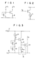
- FIG. 3 there is shown a schematic circuit diagram of a current source circuit embodying the present invention which comprises an input current source 13 for providing an input current I and NPN transistors Ql and Q2 each having its base shunted to its collector are connected in series between a positive power supply terminal 11 and a negative power supply terminal 12.
- the current source circuit is further provided with an NPN transistor Q3 having its base connected to the collector of transistor Ql and its collector connected to positive power terminal 11, a resistor 14 connected to the emitter of transistor Q3, a current supply circuit 15 connected between resistor 14 and negative power supply terminal 12 and having a current source 16 to feed a current nI which is in magnitude n times (n is a positive number, preferably a positive integer) the input current I to transistor Q3, and an NPN transistor Q4 having its base connected to a connection point between resistor 14 and current supply circuit 15, its emitter connected to negative power supply terminal 12 and providing an output current Io to its collector.
- transistors Ql and Q2 have larger emitter area than transistors Q3 and Q4, then the base-to-emitter voltage V BE of each of transistors Ql and Q2 can further be reduced, so that a smaller output current Io may be provided.
- the potential at positive power supply terminal 11 is set at +10 V, and the potential at negative power supply terminal 12 at 0 V (ground potential). It is noted that the current source circuit shown in Fig. 3 can be operated from a power supply voltage of about 1.5 V.
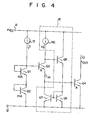
- Fig. 4 shows in particular a practical arrangement of current supply circuit 15 of Fig. 3.
- a current source 16a for providing a current nI is connected between the collector of transistor Q3 and positive power supply terminal 11
- an NPN transistor Q5 is provided which has its base connected to the collector of transistor Q3 and its collector connected to positive power supply terminal 11.
- a pair of NPN transistors Q6 and Q7 are provided which are connected in a current mirror configuration.
- Diode-connected transistor Q6 of the current mirror has its collector connected to the emitter of transistor Q5 and its emitter connected to negative power supply terminal 12.
- Transistor Q7 has its collector connected to the emitter of transistor Q3 through emitter resistor 14 thereof and its emitter connected to negative power supply terminal 12.
- transistors Ql to Q3, resistor 14, and output transistor Q4 constitute- an essential part of the low-value current source.
- Current sources 13 and 16a supply input currents I and nI to the collectors of transistors Ql and Q3, respectively.
- Transistor Q5 and current-mirror transistors Q6 and Q7 serve to make the collector current of transistor Q3 equal to nI.
- the current source circuit of this invention is arranged to make output current Io small by reducing the base-to-emitter voltage of output transistor Q4 by a voltage drop across resistor 14 caused by current supplied from current source 16a.
- collector voltage V C (Q3) of transistor Q3 is the sum of the base-to-emitter voltages V BE of transistors Q5 and Q6,
- the operation of the first circuit section to determine the output current Io will be described.
- the base-to-emitter voltage V BE and the collector current Ic of a transistor are related as follows: where V T is the electronvolt equivalent of the temperature, A is emitter area, and Is is reverse saturation current.
- the output current Io of output transistor Q4 depends on the emitter area ratio m of transistors, the current ratio n of current sources 13 and 16a, and the value Rl of resistor 14. The above is the operation of the first circuit section comprised of transistors Ql to Q4 and resistor 14.
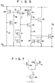
- Fig. 5 shows an experimental circuit of the current source circuit of this invention.
- I 100 ⁇ A
- the output current Io is found to be 0.10 ⁇ A from equation (17).
- the circuit section comprised of the transistors Ql to Q4 and the resistor Rl4 is the same as that of the circuit of Fig. 4, and transistors Q8 to Qll and resistors 17 and 18 form current sources 13 and 16a.
- the values of resistors 17 and 18 are 86 k ⁇ and 2.2 k ⁇ , respectively.
- the input current I is where R2 is the value of resistor 17.
- the calculated value of output current Io for estimating an error of the measured values were obtained by substituting the measured input current I and the measured voltage drop V R into the following equation which is a modification of equation (17).
- the error of current Io can be deemed about -7%, as shown in the table. This implies that the current source circuit of the present invention is sufficiently practicable and able to provide a low-value current on the order of 0.1 pA at high accuracy.
- Fig. 6 shows an output characteristic of input current versus output current. In this graph, the measured values are denoted by dots (•) and calculated values by X.
- transistors in the experimental circuit transistors in bipolar integrated transistor arrays were used.
- the used integrated circuit chips were ones packed into 16-pin dual in-line plastic package.
- pA current of 0.1 uA can effectively be handled.
- the current source circuit of the present invention is well suitable for a constant current source of a differential amplifier circuit.
- V I 1 uA
- S of transistor 022 10
- the base current I B becomes 0.1 ⁇ A when transistor Q22 is in an active condition. Accordingly, a high input impedance of about 10 M ⁇ can be provided.
Landscapes
- Engineering & Computer Science (AREA)
- Microelectronics & Electronic Packaging (AREA)
- Physics & Mathematics (AREA)
- Nonlinear Science (AREA)
- Electromagnetism (AREA)
- General Physics & Mathematics (AREA)
- Radar, Positioning & Navigation (AREA)
- Automation & Control Theory (AREA)
- Amplifiers (AREA)
- Control Of Electrical Variables (AREA)
- Dc-Dc Converters (AREA)
Applications Claiming Priority (2)
| Application Number | Priority Date | Filing Date | Title |
|---|---|---|---|
| JP56045050A JPS57160206A (en) | 1981-03-27 | 1981-03-27 | Fine current source circuit |
| JP45050/81 | 1981-03-27 |
Publications (2)
| Publication Number | Publication Date |
|---|---|
| EP0061705A1 true EP0061705A1 (de) | 1982-10-06 |
| EP0061705B1 EP0061705B1 (de) | 1984-10-31 |
Family
ID=12708526
Family Applications (1)
| Application Number | Title | Priority Date | Filing Date |
|---|---|---|---|
| EP82102427A Expired EP0061705B1 (de) | 1981-03-27 | 1982-03-24 | Schwachstromquellenkreis |
Country Status (4)
| Country | Link |
|---|---|
| US (1) | US4485313A (de) |
| EP (1) | EP0061705B1 (de) |
| JP (1) | JPS57160206A (de) |
| DE (1) | DE3261101D1 (de) |
Families Citing this family (8)
| Publication number | Priority date | Publication date | Assignee | Title |
|---|---|---|---|---|
| US4553044A (en) * | 1983-05-11 | 1985-11-12 | National Semiconductor Corporation | Integrated circuit output driver stage |
| DE3642167A1 (de) * | 1986-12-10 | 1988-06-30 | Philips Patentverwaltung | Stromspiegelschaltung |
| US4945259A (en) * | 1988-11-10 | 1990-07-31 | Burr-Brown Corporation | Bias voltage generator and method |
| JPH03128526A (ja) * | 1989-10-13 | 1991-05-31 | Nec Corp | エミッタフォロワ回路 |
| JP3156447B2 (ja) * | 1993-06-17 | 2001-04-16 | 富士通株式会社 | 半導体集積回路 |
| JP2000075942A (ja) * | 1998-08-27 | 2000-03-14 | Mitsumi Electric Co Ltd | オフセット電圧トリミング回路 |
| JP3471648B2 (ja) * | 1999-02-26 | 2003-12-02 | 富士通カンタムデバイス株式会社 | パワーアンプ回路及びそのバイアス回路 |
| JP2003347852A (ja) * | 2002-05-24 | 2003-12-05 | Toshiba Corp | バイアス回路及び半導体装置 |
Citations (2)
| Publication number | Priority date | Publication date | Assignee | Title |
|---|---|---|---|---|
| US3320439A (en) * | 1965-05-26 | 1967-05-16 | Fairchild Camera Instr Co | Low-value current source for integrated circuits |
| GB1518641A (en) * | 1976-02-26 | 1978-07-19 | Tokyo Shibaura Electric Co | Constant current circuit |
Family Cites Families (4)
| Publication number | Priority date | Publication date | Assignee | Title |
|---|---|---|---|---|
| GB1265157A (de) * | 1968-09-27 | 1972-03-01 | ||
| US3930172A (en) * | 1974-11-06 | 1975-12-30 | Nat Semiconductor Corp | Input supply independent circuit |
| JPS54161253A (en) * | 1978-06-10 | 1979-12-20 | Toshiba Corp | High-frequency amplifier circuit |
| US4350904A (en) * | 1980-09-22 | 1982-09-21 | Bell Telephone Laboratories, Incorporated | Current source with modified temperature coefficient |
-
1981
- 1981-03-27 JP JP56045050A patent/JPS57160206A/ja active Granted
-
1982
- 1982-03-23 US US06/361,092 patent/US4485313A/en not_active Expired - Lifetime
- 1982-03-24 DE DE8282102427T patent/DE3261101D1/de not_active Expired
- 1982-03-24 EP EP82102427A patent/EP0061705B1/de not_active Expired
Patent Citations (2)
| Publication number | Priority date | Publication date | Assignee | Title |
|---|---|---|---|---|
| US3320439A (en) * | 1965-05-26 | 1967-05-16 | Fairchild Camera Instr Co | Low-value current source for integrated circuits |
| GB1518641A (en) * | 1976-02-26 | 1978-07-19 | Tokyo Shibaura Electric Co | Constant current circuit |
Non-Patent Citations (1)
| Title |
|---|
| IBM TECHNICAL DISCLOSURE BULLETIN, vol. 14, no. 4, September 1971, pages 1039 and 1040, New York (USA); * |
Also Published As
| Publication number | Publication date |
|---|---|
| DE3261101D1 (en) | 1984-12-06 |
| EP0061705B1 (de) | 1984-10-31 |
| US4485313A (en) | 1984-11-27 |
| JPS6155284B2 (de) | 1986-11-27 |
| JPS57160206A (en) | 1982-10-02 |
Similar Documents
| Publication | Publication Date | Title |
|---|---|---|
| US4329639A (en) | Low voltage current mirror | |
| US4507573A (en) | Current source circuit for producing a small value output current proportional to an input current | |
| US4567444A (en) | Current mirror circuit with control means for establishing an input-output current ratio | |
| US4302718A (en) | Reference potential generating circuits | |
| EP0155720B1 (de) | Kaskadenstromquellenanordnung | |
| US4524318A (en) | Band gap voltage reference circuit | |
| US4119869A (en) | Constant current circuit | |
| EP0419819B1 (de) | Stromspiegel | |
| GB2086682A (en) | Current amplifier | |
| US4647841A (en) | Low voltage, high precision current source | |
| US4533845A (en) | Current limit technique for multiple-emitter vertical power transistor | |
| EP0124918B1 (de) | Stromquellenanordnung | |
| US4677368A (en) | Precision thermal current source | |
| EP0606144A1 (de) | Transkonduktanz-Operationsverstärker mit hoher Aussteuerung | |
| EP0061705B1 (de) | Schwachstromquellenkreis | |
| US4590419A (en) | Circuit for generating a temperature-stabilized reference voltage | |
| US3868581A (en) | Current amplifier | |
| JP2869664B2 (ja) | 電流増幅器 | |
| KR920009548B1 (ko) | 전류원 장치 | |
| US4352057A (en) | Constant current source | |
| US4329598A (en) | Bias generator | |
| US4661781A (en) | Amplifier with floating inverting and non-inverting inputs and stabilized direct output voltage level | |
| EP0264563B1 (de) | Spannungsregler mit Präzisionsthermostromquelle | |
| EP0110720B1 (de) | Stromspiegelschaltungsanordnung | |
| EP0064126A2 (de) | Differentialverstärker |
Legal Events
| Date | Code | Title | Description |
|---|---|---|---|
| PUAI | Public reference made under article 153(3) epc to a published international application that has entered the european phase |
Free format text: ORIGINAL CODE: 0009012 |
|
| 17P | Request for examination filed |
Effective date: 19820324 |
|
| AK | Designated contracting states |
Designated state(s): DE FR GB |
|
| GRAA | (expected) grant |
Free format text: ORIGINAL CODE: 0009210 |
|
| RAP1 | Party data changed (applicant data changed or rights of an application transferred) |
Owner name: KABUSHIKI KAISHA TOSHIBA |
|
| AK | Designated contracting states |
Designated state(s): DE FR GB |
|
| REF | Corresponds to: |
Ref document number: 3261101 Country of ref document: DE Date of ref document: 19841206 |
|
| ET | Fr: translation filed | ||
| PLBE | No opposition filed within time limit |
Free format text: ORIGINAL CODE: 0009261 |
|
| STAA | Information on the status of an ep patent application or granted ep patent |
Free format text: STATUS: NO OPPOSITION FILED WITHIN TIME LIMIT |
|
| 26N | No opposition filed | ||
| REG | Reference to a national code |
Ref country code: GB Ref legal event code: 746 |
|
| PGFP | Annual fee paid to national office [announced via postgrant information from national office to epo] |
Ref country code: FR Payment date: 19970313 Year of fee payment: 16 |
|
| PGFP | Annual fee paid to national office [announced via postgrant information from national office to epo] |
Ref country code: GB Payment date: 19970317 Year of fee payment: 16 |
|
| PGFP | Annual fee paid to national office [announced via postgrant information from national office to epo] |
Ref country code: DE Payment date: 19970401 Year of fee payment: 16 |
|
| PG25 | Lapsed in a contracting state [announced via postgrant information from national office to epo] |
Ref country code: GB Free format text: LAPSE BECAUSE OF NON-PAYMENT OF DUE FEES Effective date: 19980324 |
|
| PG25 | Lapsed in a contracting state [announced via postgrant information from national office to epo] |
Ref country code: FR Free format text: THE PATENT HAS BEEN ANNULLED BY A DECISION OF A NATIONAL AUTHORITY Effective date: 19980331 |
|
| GBPC | Gb: european patent ceased through non-payment of renewal fee |
Effective date: 19980324 |
|
| PG25 | Lapsed in a contracting state [announced via postgrant information from national office to epo] |
Ref country code: DE Free format text: LAPSE BECAUSE OF NON-PAYMENT OF DUE FEES Effective date: 19981201 |
|
| REG | Reference to a national code |
Ref country code: FR Ref legal event code: ST |