EP0058023B1 - Process of treating anodic oxide film, printed wiring board and process of making the same - Google Patents
Process of treating anodic oxide film, printed wiring board and process of making the same Download PDFInfo
- Publication number
- EP0058023B1 EP0058023B1 EP82300465A EP82300465A EP0058023B1 EP 0058023 B1 EP0058023 B1 EP 0058023B1 EP 82300465 A EP82300465 A EP 82300465A EP 82300465 A EP82300465 A EP 82300465A EP 0058023 B1 EP0058023 B1 EP 0058023B1
- Authority
- EP
- European Patent Office
- Prior art keywords
- anodic oxide
- oxide film
- process according
- compound
- film
- Prior art date
- Legal status (The legal status is an assumption and is not a legal conclusion. Google has not performed a legal analysis and makes no representation as to the accuracy of the status listed.)
- Expired
Links
- 239000010407 anodic oxide Substances 0.000 title claims description 101
- 238000000034 method Methods 0.000 title claims description 32
- 150000001875 compounds Chemical class 0.000 claims description 43
- 229910052782 aluminium Inorganic materials 0.000 claims description 37
- 239000000243 solution Substances 0.000 claims description 35
- XAGFODPZIPBFFR-UHFFFAOYSA-N aluminium Chemical compound [Al] XAGFODPZIPBFFR-UHFFFAOYSA-N 0.000 claims description 34
- 239000004020 conductor Substances 0.000 claims description 22
- MUBZPKHOEPUJKR-UHFFFAOYSA-N Oxalic acid Chemical compound OC(=O)C(O)=O MUBZPKHOEPUJKR-UHFFFAOYSA-N 0.000 claims description 21
- 229910052751 metal Inorganic materials 0.000 claims description 20
- 239000002184 metal Substances 0.000 claims description 20
- 229920000642 polymer Polymers 0.000 claims description 16
- 238000010438 heat treatment Methods 0.000 claims description 15
- XLYOFNOQVPJJNP-UHFFFAOYSA-N water Substances O XLYOFNOQVPJJNP-UHFFFAOYSA-N 0.000 claims description 15
- 239000000463 material Substances 0.000 claims description 14
- 229910000838 Al alloy Inorganic materials 0.000 claims description 13
- 229910052710 silicon Inorganic materials 0.000 claims description 12
- 238000007743 anodising Methods 0.000 claims description 11
- 238000005470 impregnation Methods 0.000 claims description 11
- 238000007789 sealing Methods 0.000 claims description 9
- 238000001962 electrophoresis Methods 0.000 claims description 8
- 239000000203 mixture Substances 0.000 claims description 8
- 239000003960 organic solvent Substances 0.000 claims description 8
- 239000010703 silicon Substances 0.000 claims description 8
- 239000004411 aluminium Substances 0.000 claims description 7
- 235000006408 oxalic acid Nutrition 0.000 claims description 7
- 239000008151 electrolyte solution Substances 0.000 claims description 6
- 229910052719 titanium Inorganic materials 0.000 claims description 6
- -1 amino, mercapto Chemical class 0.000 claims description 4
- 125000002496 methyl group Chemical group [H]C([H])([H])* 0.000 claims description 4
- 125000001997 phenyl group Chemical group [H]C1=C([H])C([H])=C(*)C([H])=C1[H] 0.000 claims description 4
- 229910052726 zirconium Inorganic materials 0.000 claims description 4
- QGZKDVFQNNGYKY-UHFFFAOYSA-O Ammonium Chemical compound [NH4+] QGZKDVFQNNGYKY-UHFFFAOYSA-O 0.000 claims description 3
- 229910000861 Mg alloy Inorganic materials 0.000 claims description 3
- 150000003863 ammonium salts Chemical class 0.000 claims description 3
- 125000000962 organic group Chemical group 0.000 claims description 3
- 159000000000 sodium salts Chemical class 0.000 claims description 3
- 239000004593 Epoxy Substances 0.000 claims description 2
- FKNQFGJONOIPTF-UHFFFAOYSA-N Sodium cation Chemical compound [Na+] FKNQFGJONOIPTF-UHFFFAOYSA-N 0.000 claims description 2
- 125000003668 acetyloxy group Chemical group [H]C([H])([H])C(=O)O[*] 0.000 claims description 2
- 125000003545 alkoxy group Chemical group 0.000 claims description 2
- 229910052796 boron Inorganic materials 0.000 claims description 2
- 125000003700 epoxy group Chemical group 0.000 claims description 2
- 229910052732 germanium Inorganic materials 0.000 claims description 2
- 229910052698 phosphorus Inorganic materials 0.000 claims description 2
- 229910001415 sodium ion Inorganic materials 0.000 claims description 2
- 125000000391 vinyl group Chemical group [H]C([*])=C([H])[H] 0.000 claims description 2
- 229920002554 vinyl polymer Polymers 0.000 claims description 2
- 229910000789 Aluminium-silicon alloy Inorganic materials 0.000 claims 1
- XAEFZNCEHLXOMS-UHFFFAOYSA-M potassium benzoate Chemical compound [K+].[O-]C(=O)C1=CC=CC=C1 XAEFZNCEHLXOMS-UHFFFAOYSA-M 0.000 claims 1
- 150000002894 organic compounds Chemical class 0.000 description 48
- 238000011282 treatment Methods 0.000 description 23
- 238000005336 cracking Methods 0.000 description 20
- 238000010292 electrical insulation Methods 0.000 description 16
- PXHVJJICTQNCMI-UHFFFAOYSA-N Nickel Chemical compound [Ni] PXHVJJICTQNCMI-UHFFFAOYSA-N 0.000 description 14
- LFQSCWFLJHTTHZ-UHFFFAOYSA-N Ethanol Chemical compound CCO LFQSCWFLJHTTHZ-UHFFFAOYSA-N 0.000 description 12
- 239000010953 base metal Substances 0.000 description 12
- 229910000676 Si alloy Inorganic materials 0.000 description 11
- CSDREXVUYHZDNP-UHFFFAOYSA-N alumanylidynesilicon Chemical compound [Al].[Si] CSDREXVUYHZDNP-UHFFFAOYSA-N 0.000 description 11
- 238000002048 anodisation reaction Methods 0.000 description 8
- 230000015556 catabolic process Effects 0.000 description 8
- 238000006731 degradation reaction Methods 0.000 description 8
- 238000009413 insulation Methods 0.000 description 8
- XUIMIQQOPSSXEZ-UHFFFAOYSA-N Silicon Chemical compound [Si] XUIMIQQOPSSXEZ-UHFFFAOYSA-N 0.000 description 7
- 229910052759 nickel Inorganic materials 0.000 description 7
- ZWEHNKRNPOVVGH-UHFFFAOYSA-N 2-Butanone Chemical compound CCC(C)=O ZWEHNKRNPOVVGH-UHFFFAOYSA-N 0.000 description 6
- CSCPPACGZOOCGX-UHFFFAOYSA-N Acetone Chemical compound CC(C)=O CSCPPACGZOOCGX-UHFFFAOYSA-N 0.000 description 6
- OKKJLVBELUTLKV-UHFFFAOYSA-N Methanol Chemical compound OC OKKJLVBELUTLKV-UHFFFAOYSA-N 0.000 description 6
- 229910045601 alloy Inorganic materials 0.000 description 6
- 239000000956 alloy Substances 0.000 description 6
- 230000007797 corrosion Effects 0.000 description 6
- 238000005260 corrosion Methods 0.000 description 6
- 238000007747 plating Methods 0.000 description 6
- 239000002861 polymer material Substances 0.000 description 6
- 239000011347 resin Substances 0.000 description 6
- 229920005989 resin Polymers 0.000 description 6
- 150000002739 metals Chemical class 0.000 description 5
- 238000006116 polymerization reaction Methods 0.000 description 5
- 239000000126 substance Substances 0.000 description 5
- 238000005406 washing Methods 0.000 description 5
- FYYHWMGAXLPEAU-UHFFFAOYSA-N Magnesium Chemical compound [Mg] FYYHWMGAXLPEAU-UHFFFAOYSA-N 0.000 description 4
- 239000011248 coating agent Substances 0.000 description 4
- 238000000576 coating method Methods 0.000 description 4
- 238000001035 drying Methods 0.000 description 4
- 229910052749 magnesium Inorganic materials 0.000 description 4
- 239000011777 magnesium Substances 0.000 description 4
- 239000010936 titanium Substances 0.000 description 4
- XEKOWRVHYACXOJ-UHFFFAOYSA-N Ethyl acetate Chemical compound CCOC(C)=O XEKOWRVHYACXOJ-UHFFFAOYSA-N 0.000 description 3
- LYCAIKOWRPUZTN-UHFFFAOYSA-N Ethylene glycol Chemical compound OCCO LYCAIKOWRPUZTN-UHFFFAOYSA-N 0.000 description 3
- ZMXDDKWLCZADIW-UHFFFAOYSA-N N,N-Dimethylformamide Chemical compound CN(C)C=O ZMXDDKWLCZADIW-UHFFFAOYSA-N 0.000 description 3
- VYPSYNLAJGMNEJ-UHFFFAOYSA-N Silicium dioxide Chemical compound O=[Si]=O VYPSYNLAJGMNEJ-UHFFFAOYSA-N 0.000 description 3
- HEMHJVSKTPXQMS-UHFFFAOYSA-M Sodium hydroxide Chemical compound [OH-].[Na+] HEMHJVSKTPXQMS-UHFFFAOYSA-M 0.000 description 3
- 230000004913 activation Effects 0.000 description 3
- 230000000052 comparative effect Effects 0.000 description 3
- 230000000873 masking effect Effects 0.000 description 3
- PIBWKRNGBLPSSY-UHFFFAOYSA-L palladium(II) chloride Chemical compound Cl[Pd]Cl PIBWKRNGBLPSSY-UHFFFAOYSA-L 0.000 description 3
- 239000011856 silicon-based particle Substances 0.000 description 3
- TXUICONDJPYNPY-UHFFFAOYSA-N (1,10,13-trimethyl-3-oxo-4,5,6,7,8,9,11,12,14,15,16,17-dodecahydrocyclopenta[a]phenanthren-17-yl) heptanoate Chemical compound C1CC2CC(=O)C=C(C)C2(C)C2C1C1CCC(OC(=O)CCCCCC)C1(C)CC2 TXUICONDJPYNPY-UHFFFAOYSA-N 0.000 description 2
- RYGMFSIKBFXOCR-UHFFFAOYSA-N Copper Chemical compound [Cu] RYGMFSIKBFXOCR-UHFFFAOYSA-N 0.000 description 2
- KFZMGEQAYNKOFK-UHFFFAOYSA-N Isopropanol Chemical compound CC(C)O KFZMGEQAYNKOFK-UHFFFAOYSA-N 0.000 description 2
- XBDQKXXYIPTUBI-UHFFFAOYSA-M Propionate Chemical compound CCC([O-])=O XBDQKXXYIPTUBI-UHFFFAOYSA-M 0.000 description 2
- 229910021626 Tin(II) chloride Inorganic materials 0.000 description 2
- RTAQQCXQSZGOHL-UHFFFAOYSA-N Titanium Chemical compound [Ti] RTAQQCXQSZGOHL-UHFFFAOYSA-N 0.000 description 2
- 239000000654 additive Substances 0.000 description 2
- NGPGDYLVALNKEG-UHFFFAOYSA-N azanium;azane;2,3,4-trihydroxy-4-oxobutanoate Chemical compound [NH4+].[NH4+].[O-]C(=O)C(O)C(O)C([O-])=O NGPGDYLVALNKEG-UHFFFAOYSA-N 0.000 description 2
- 238000009835 boiling Methods 0.000 description 2
- 229910052802 copper Inorganic materials 0.000 description 2
- 239000010949 copper Substances 0.000 description 2
- 238000000151 deposition Methods 0.000 description 2
- SWXVUIWOUIDPGS-UHFFFAOYSA-N diacetone alcohol Chemical compound CC(=O)CC(C)(C)O SWXVUIWOUIDPGS-UHFFFAOYSA-N 0.000 description 2
- 238000007772 electroless plating Methods 0.000 description 2
- 230000007062 hydrolysis Effects 0.000 description 2
- 238000006460 hydrolysis reaction Methods 0.000 description 2
- 238000004519 manufacturing process Methods 0.000 description 2
- 150000002902 organometallic compounds Chemical class 0.000 description 2
- 230000000379 polymerizing effect Effects 0.000 description 2
- 229920001296 polysiloxane Polymers 0.000 description 2
- 239000011148 porous material Substances 0.000 description 2
- 239000010935 stainless steel Substances 0.000 description 2
- 229910001220 stainless steel Inorganic materials 0.000 description 2
- 239000001119 stannous chloride Substances 0.000 description 2
- 235000011150 stannous chloride Nutrition 0.000 description 2
- 229910052715 tantalum Inorganic materials 0.000 description 2
- GUVRBAGPIYLISA-UHFFFAOYSA-N tantalum atom Chemical compound [Ta] GUVRBAGPIYLISA-UHFFFAOYSA-N 0.000 description 2
- CPUDPFPXCZDNGI-UHFFFAOYSA-N triethoxy(methyl)silane Chemical compound CCO[Si](C)(OCC)OCC CPUDPFPXCZDNGI-UHFFFAOYSA-N 0.000 description 2
- RYHBNJHYFVUHQT-UHFFFAOYSA-N 1,4-Dioxane Chemical compound C1COCCO1 RYHBNJHYFVUHQT-UHFFFAOYSA-N 0.000 description 1
- DDFHBQSCUXNBSA-UHFFFAOYSA-N 5-(5-carboxythiophen-2-yl)thiophene-2-carboxylic acid Chemical compound S1C(C(=O)O)=CC=C1C1=CC=C(C(O)=O)S1 DDFHBQSCUXNBSA-UHFFFAOYSA-N 0.000 description 1
- 229910000553 6063 aluminium alloy Inorganic materials 0.000 description 1
- PNEYBMLMFCGWSK-UHFFFAOYSA-N Alumina Chemical compound [O-2].[O-2].[O-2].[Al+3].[Al+3] PNEYBMLMFCGWSK-UHFFFAOYSA-N 0.000 description 1
- ATRRKUHOCOJYRX-UHFFFAOYSA-N Ammonium bicarbonate Chemical compound [NH4+].OC([O-])=O ATRRKUHOCOJYRX-UHFFFAOYSA-N 0.000 description 1
- VHUUQVKOLVNVRT-UHFFFAOYSA-N Ammonium hydroxide Chemical compound [NH4+].[OH-] VHUUQVKOLVNVRT-UHFFFAOYSA-N 0.000 description 1
- YPSWAXOVJWXMGI-UHFFFAOYSA-N COC(C[Sn])OC Chemical compound COC(C[Sn])OC YPSWAXOVJWXMGI-UHFFFAOYSA-N 0.000 description 1
- GLFYWGWWUUNJTL-UHFFFAOYSA-N C[O-].C[O-].C[O-].C[Ge+3] Chemical compound C[O-].C[O-].C[O-].C[Ge+3] GLFYWGWWUUNJTL-UHFFFAOYSA-N 0.000 description 1
- QAOWNCQODCNURD-UHFFFAOYSA-N Sulfuric acid Chemical compound OS(O)(=O)=O QAOWNCQODCNURD-UHFFFAOYSA-N 0.000 description 1
- KXKVLQRXCPHEJC-UHFFFAOYSA-N acetic acid trimethyl ester Natural products COC(C)=O KXKVLQRXCPHEJC-UHFFFAOYSA-N 0.000 description 1
- 239000002253 acid Substances 0.000 description 1
- 230000000996 additive effect Effects 0.000 description 1
- 239000000853 adhesive Substances 0.000 description 1
- 230000001070 adhesive effect Effects 0.000 description 1
- 239000001099 ammonium carbonate Substances 0.000 description 1
- 235000012501 ammonium carbonate Nutrition 0.000 description 1
- 239000000908 ammonium hydroxide Substances 0.000 description 1
- 239000012298 atmosphere Substances 0.000 description 1
- 230000004888 barrier function Effects 0.000 description 1
- 230000015572 biosynthetic process Effects 0.000 description 1
- 239000004566 building material Substances 0.000 description 1
- 238000006243 chemical reaction Methods 0.000 description 1
- 239000008119 colloidal silica Substances 0.000 description 1
- 238000005238 degreasing Methods 0.000 description 1
- 230000008021 deposition Effects 0.000 description 1
- 238000009792 diffusion process Methods 0.000 description 1
- ZJUSUEINLFVURI-UHFFFAOYSA-N dimethoxy(dimethyl)germane Chemical compound CO[Ge](C)(C)OC ZJUSUEINLFVURI-UHFFFAOYSA-N 0.000 description 1
- 238000009826 distribution Methods 0.000 description 1
- 238000005868 electrolysis reaction Methods 0.000 description 1
- 238000005530 etching Methods 0.000 description 1
- 238000011049 filling Methods 0.000 description 1
- WBJINCZRORDGAQ-UHFFFAOYSA-N formic acid ethyl ester Natural products CCOC=O WBJINCZRORDGAQ-UHFFFAOYSA-N 0.000 description 1
- 238000013007 heat curing Methods 0.000 description 1
- 230000036571 hydration Effects 0.000 description 1
- 238000006703 hydration reaction Methods 0.000 description 1
- 238000007733 ion plating Methods 0.000 description 1
- 150000002500 ions Chemical class 0.000 description 1
- 229910044991 metal oxide Inorganic materials 0.000 description 1
- 125000000082 organogermanium group Chemical group 0.000 description 1
- 150000003961 organosilicon compounds Chemical class 0.000 description 1
- TWNQGVIAIRXVLR-UHFFFAOYSA-N oxo(oxoalumanyloxy)alumane Chemical compound O=[Al]O[Al]=O TWNQGVIAIRXVLR-UHFFFAOYSA-N 0.000 description 1
- 239000003973 paint Substances 0.000 description 1
- 150000003013 phosphoric acid derivatives Chemical class 0.000 description 1
- 229910000077 silane Inorganic materials 0.000 description 1
- 150000003377 silicon compounds Chemical class 0.000 description 1
- 239000000377 silicon dioxide Substances 0.000 description 1
- FQENQNTWSFEDLI-UHFFFAOYSA-J sodium diphosphate Chemical compound [Na+].[Na+].[Na+].[Na+].[O-]P([O-])(=O)OP([O-])([O-])=O FQENQNTWSFEDLI-UHFFFAOYSA-J 0.000 description 1
- 229940048086 sodium pyrophosphate Drugs 0.000 description 1
- 238000004544 sputter deposition Methods 0.000 description 1
- 239000000758 substrate Substances 0.000 description 1
- 239000001117 sulphuric acid Substances 0.000 description 1
- 235000011149 sulphuric acid Nutrition 0.000 description 1
- 239000004094 surface-active agent Substances 0.000 description 1
- 235000019818 tetrasodium diphosphate Nutrition 0.000 description 1
- 239000001577 tetrasodium phosphonato phosphate Substances 0.000 description 1
- 230000008646 thermal stress Effects 0.000 description 1
- JCVQKRGIASEUKR-UHFFFAOYSA-N triethoxy(phenyl)silane Chemical compound CCO[Si](OCC)(OCC)C1=CC=CC=C1 JCVQKRGIASEUKR-UHFFFAOYSA-N 0.000 description 1
- 238000007738 vacuum evaporation Methods 0.000 description 1
- 238000004804 winding Methods 0.000 description 1
Images

Classifications
-
- H—ELECTRICITY
- H05—ELECTRIC TECHNIQUES NOT OTHERWISE PROVIDED FOR
- H05K—PRINTED CIRCUITS; CASINGS OR CONSTRUCTIONAL DETAILS OF ELECTRIC APPARATUS; MANUFACTURE OF ASSEMBLAGES OF ELECTRICAL COMPONENTS
- H05K1/00—Printed circuits
- H05K1/02—Details
- H05K1/03—Use of materials for the substrate
- H05K1/05—Insulated conductive substrates, e.g. insulated metal substrate
- H05K1/053—Insulated conductive substrates, e.g. insulated metal substrate the metal substrate being covered by an inorganic insulating layer
-
- C—CHEMISTRY; METALLURGY
- C25—ELECTROLYTIC OR ELECTROPHORETIC PROCESSES; APPARATUS THEREFOR
- C25D—PROCESSES FOR THE ELECTROLYTIC OR ELECTROPHORETIC PRODUCTION OF COATINGS; ELECTROFORMING; APPARATUS THEREFOR
- C25D11/00—Electrolytic coating by surface reaction, i.e. forming conversion layers
- C25D11/02—Anodisation
-
- C—CHEMISTRY; METALLURGY
- C25—ELECTROLYTIC OR ELECTROPHORETIC PROCESSES; APPARATUS THEREFOR
- C25D—PROCESSES FOR THE ELECTROLYTIC OR ELECTROPHORETIC PRODUCTION OF COATINGS; ELECTROFORMING; APPARATUS THEREFOR
- C25D11/00—Electrolytic coating by surface reaction, i.e. forming conversion layers
- C25D11/02—Anodisation
- C25D11/04—Anodisation of aluminium or alloys based thereon
- C25D11/18—After-treatment, e.g. pore-sealing
-
- C—CHEMISTRY; METALLURGY
- C25—ELECTROLYTIC OR ELECTROPHORETIC PROCESSES; APPARATUS THEREFOR
- C25D—PROCESSES FOR THE ELECTROLYTIC OR ELECTROPHORETIC PRODUCTION OF COATINGS; ELECTROFORMING; APPARATUS THEREFOR
- C25D11/00—Electrolytic coating by surface reaction, i.e. forming conversion layers
- C25D11/02—Anodisation
- C25D11/04—Anodisation of aluminium or alloys based thereon
- C25D11/18—After-treatment, e.g. pore-sealing
- C25D11/24—Chemical after-treatment
- C25D11/246—Chemical after-treatment for sealing layers
-
- H—ELECTRICITY
- H01—ELECTRIC ELEMENTS
- H01B—CABLES; CONDUCTORS; INSULATORS; SELECTION OF MATERIALS FOR THEIR CONDUCTIVE, INSULATING OR DIELECTRIC PROPERTIES
- H01B3/00—Insulators or insulating bodies characterised by the insulating materials; Selection of materials for their insulating or dielectric properties
- H01B3/18—Insulators or insulating bodies characterised by the insulating materials; Selection of materials for their insulating or dielectric properties mainly consisting of organic substances
- H01B3/30—Insulators or insulating bodies characterised by the insulating materials; Selection of materials for their insulating or dielectric properties mainly consisting of organic substances plastics; resins; waxes
- H01B3/46—Insulators or insulating bodies characterised by the insulating materials; Selection of materials for their insulating or dielectric properties mainly consisting of organic substances plastics; resins; waxes silicones
-
- H—ELECTRICITY
- H05—ELECTRIC TECHNIQUES NOT OTHERWISE PROVIDED FOR
- H05K—PRINTED CIRCUITS; CASINGS OR CONSTRUCTIONAL DETAILS OF ELECTRIC APPARATUS; MANUFACTURE OF ASSEMBLAGES OF ELECTRICAL COMPONENTS
- H05K2203/00—Indexing scheme relating to apparatus or processes for manufacturing printed circuits covered by H05K3/00
- H05K2203/03—Metal processing
- H05K2203/0315—Oxidising metal
-
- H—ELECTRICITY
- H05—ELECTRIC TECHNIQUES NOT OTHERWISE PROVIDED FOR
- H05K—PRINTED CIRCUITS; CASINGS OR CONSTRUCTIONAL DETAILS OF ELECTRIC APPARATUS; MANUFACTURE OF ASSEMBLAGES OF ELECTRICAL COMPONENTS
- H05K2203/00—Indexing scheme relating to apparatus or processes for manufacturing printed circuits covered by H05K3/00
- H05K2203/11—Treatments characterised by their effect, e.g. heating, cooling, roughening
- H05K2203/1147—Sealing or impregnating, e.g. of pores
Definitions
- This invention relates to a process for producing a treated anodic oxide film on a valve metal base, by anodizing the valve metal base to form thereon an anodic oxide film having micropores therein, applying a polymerisable compound thereto and polymerising the compound.
- the treated film has high heat radiance, heat resistance and electrical insulation.
- the invention also provides a method of making a printed wiring board using such anodic oxide film.
- Anodic oxide films formed on valve metals such as aluminium, titanium, magnesium, tantalum, and their alloys are electrically insulating metallic oxide films which are conversion-coated on their surfaces.
- the anodic oxide films have homogeneous composition and are excellent in adhesion to their base metal, corrosion resistance and thermal conductivity.
- metals having anodic oxide films formed thereon are widely used for printed wiring boards of electronic instruments, radiator plates of electronic parts, electrically insulative heat sinks, insulated wires, building materials and the like.
- thick anodic oxide films are used for such use, but for the oxide films having a thickness of not less than several microns a great number of micropores are necessarily formed therein.
- micropores are very small holes having a diameter of several hundred angstroms which reach the barrier layer of the anodic oxide film. Entrance of moisture in the air into and residue of anodizing electrolytic solution in the micropores make it impossible to obtain a thick anodic oxide film having sufficiently high electrical insulation and corrosion resistance.
- sealing treatment can be rendered on the micropores for sealing thereof by the use of steam or boiling water. However by such treatment the anodic oxide film is subjected to hydration and cracks are produced in this hydrated film merely by heating it up to around 150°C.
- micropores For the sealing of the micropores there has been proposed another treatment that the micropores are impregnated with resins and the like.
- micropores of almite films for instance, have a very small diameter of several tens of nonometres and a depth of several ten micrometers and hence it in practice impossible to impregnate the micropores with resins to their innermost portions because of viscosity thereof.
- US-A-3 340 161 discloses the treatment of anodised aluminium, first with aqueous colloidal silica to deposit a thin silica film on top of the anodic oxide layer, and then with an organopolysiloxane solution, before drying and baking to cure the silicone' coating which seals the pores of the anodised film.
- the coated anodised aluminium substrate for an electrical printed circuit board which is resistant to high temperatures and is relatively inexpensive to produce.
- US-A-3 935 349 disclosed a method of coating an anodic oxide layer on aluminium which comprises treating the layer with a silane compound, applying a thermo-setting resin paint and then heat-curing the resin.
- a base material having an anodic oxide film impregnated with polymerized compound which is excellent in heat radiance, heat resistance and electric insulation, and is hence useful for the printed wiring board, electrically insulative heat sink, heat-resistant insulated wire and the like.
- the printed wiring board comprises a base metal plate having an anodic oxide film formed thereon with micropores filled and sealed with an organometallic compound polymer material produced according to the process of the present invention, and a conductor circuit disposed on the compound polymer material.
- the above printed wiring board is produced according to a process which comprises the steps of: anodizing a base metal plate of a valve metal to form an anodic oxide film thereon; impregnating the anodic oxide film with a polymerizable compound, and polymerizing and hardening the polymerizable compound to form a compound polymer material thereby filling and sealing the micropores of the anodic oxide film, and thereafter disposing a conductor circuit on the polymer material.
- the metals and their alloys employed as base metal in the present invention are anodizable valve metals such as aluminum, magnesium, titanium, tantalum, and their alloys.
- Aluminum or aluminum alloy base materials employed in the present invention include, for example, JIS-1 (A A1100) aluminum, high tensile aluminum alloy plate, corrosion-resistant aluminum alloy, and the like. Use may be made of aluminum-silicon alloy which contains not more than about 20% by weight, preferably about 5 to 15% by weight of silicon and if necessary a small amount of additives.
- the aluminum-silicon alloy has a property that its thermal expansion coefficient is in inverse proportion to silicon content in the alloy. For example, aluminum-silicon alloy containing 11 % by weight of silicon has a thermal expansion coefficient of 1.97xlO-', while aluminum and aluminum oxide have those of about 25x10- 6 and about 6x10- 6 , respectively.
- the aluminum-silicon alloy contains silicon particles dispersed in an aluminum continuous phase and when anodized, the silicon particles remain in an anodic oxide film.
- the silicon particles serve to prevent or at least minimize the cracking of the anodic oxide film. Beyond about 20% by weight of silicon the insulating property of the anodic oxide film is largely degraded and is not acceptable for practical use.
- the magnesium material employed in the present invention may be any of those capable of forming an anodic oxide film including magnesium alloy such as the conventional ASTM AZ31C and AZ61A.
- a through hole, opening for attaching an electrical or electronic parts and the like may be previously formed in the base plate of valve metal.
- the base materials of the previously-mentioned metals or their alloys are anodized in an electrolytic bath such as sulphuric acid, oxalic acid and the like to form an anodic oxide film thereon.
- an anodic oxide film having a thickness of about 5 to about 200 ⁇ m is formed.
- Anodizing treatment of base materials of aluminum or aluminum alloy is carried out in an electrolytic bath containing, for example, an ammonium salt such as ammonium tartrate, ammonium hydroxide, ammonium carbonate, and ammonium fluoride, or a sodium salt such as sodium hydroxide, and sodium pyrophosphate.
- the ammonium ion concentration in the electrolytic bath may be within a range of about 5 to about 80 g/I, and preferably about 5 to 40 g/I.
- the sodium ion concentration in the electrolytic bath may be within a range of about 1 to 30 g/l, and preferably about 1 to about 20 g/I.
- the bath temperature may be within a range of about 5 to 40°C, and current density may be of about 0.5 to 10 AJdm 2 .
- temperatures above which cracking of the films occurs are raised, and heat resistance of the films is enhanced.
- the anodizing treatment may be carried out by the use of about 4 to about 25% by weight, preferably about 7 to about 20% by weight, of aqueous oxalic acid solution as an electrolytic bath under the conditions of a bath temperature of about 20 to 50°C and a current density of about 0.5 to 10 A/dm 2 , preferably 1.5 to 5 A/dm 2 with an aluminum plate or aluminum alloy plate being made the anode and a suitable inert conductor such as stainless steel piece the cathode.
- a bath temperature of about 20 to 50°C and a current density of about 0.5 to 10 A/dm 2 , preferably 1.5 to 5 A/dm 2
- an aluminum plate or aluminum alloy plate being made the anode and a suitable inert conductor such as stainless steel piece the cathode.
- the process of forming an anodic oxide film on the magnesium base material used in the present invention may be any one of the conventional treatments such as HAE (U.S. Patent 2,880,148, ASTM Class II Type III), Dow Anodizing (ASTM Class II type II) and the like. (See for example "Kinzoku Hyomen Gijutsu Binran” published by Nikkan Kogyo Shinbunsha, Japan, 1976, pp. 710-711).
- anodic oxide film is impregnated with a polymerizable compound. Before this impregnation, if needed, the anodic oxide film may be subjected to the well-known sealing treatment by the use of steam, boiling water, and the like.
- the polymerizable compounds used in the present invention include, for example, organosilicon compounds such as phenyltriethoxysilane, methyltriethoxysilane, vinyltris((3-methoxyethoxy) siiane, P - (3,4 - epoxy - cyclohexyl)ethyltrimethoxysilane, and y-glycideoxypropyltrimethoxysilane; organotitanium compounds; organoalumirium compounds; organozirconium compounds; organic phosphate compounds; organoboron compounds; organogermanium compounds such as dimethyloxydimethyl germanium, and methylgermanium trimethoxide; dimethyloxyethyl tin; and their derivatives and oligomers.
- organosilicon compounds such as phenyltriethoxysilane, methyltriethoxysilane, vinyltris((3-methoxyethoxy) siiane, P -
- the polymerizable compounds employed in the present invention preferably contain Si, Al, Zr or Ti as M. Further the compound contains preferably methyl and/or phenyl group as an organic group for improving heat resistance of the anodic oxide film.
- the organic compound of which hydrolysis takes place gradually is preferred in the present invention.
- the above-mentioned polymerizable organic compounds are used in the form of a solution in organic solvent such as methanol, ethanol, acetone, ethyl acetate, and methyl ethyl ketone; water; or mixture of water and a water soluble organic solvent.
- Such soluble organic solvent may include methanol, ethanol, isopropanol, acetone, dioxane, ethylene glycol, methyl acetate, methyl ethyl ketone, diacetone alcohol, ethyl formate, dimethylformamide, and the like.
- An additive such as surfactant may be added to the soluble organic solvent, if needed.
- the impregnation with the polymerizable organic compound is carried out by vacuum impregnate treatment.
- the impregnation is achieved by electrophoresis or electropermeation in which an anodic oxide film is immersed in a solution of the polymerizable organic compound in water or a mixture of water and a water soluble organic solvent, and then direct current is applied between the anodic oxide film as the anode and a suitable inert conductor such as stainless steel piece as the cathode so that the micropores of the film are fully impregnated with the organic compound from their bottom to open end.
- a suitable inert conductor such as stainless steel piece as the cathode
- the solution of the organic compound adhered to the surface of the film is sufficiently wiped off to provide a high thermal conductivity or is remained without wiping to provide a high electrical insulation.
- the anodic oxide film is dried up to remove the water and the organic solvent in the solution after the polymerizable organic compound is fully adhered to and deposited in the micropores or on the surface of the film.
- the organic compound thus deposited is polymerized by conventional treatment such as heating, so that a compact organic compound polymer material is obtained.
- the organic compound polymer has high affinity to the anodic oxide film, and hence it strongly adheres to the walls of the micropores or the surface of the film, and fills compactly the micropores or positively cover the surface.
- the anodic oxide film subjected to the sealing treatment with an organic compound according to the present invention has micropores compactly filled with the organic compound polymer and may have a surface covered with the polymer, and thus very high electric insulation is given to the anodic oxide film.
- the organic compound polymer material can be deposited only in the micropores of the anodic oxide film by previously wiping off the solution of the organic compound sticked to the surface of the film. Also in this case the film has sufficient electrical insulation of the film even up to about 150°C as well as excellent thermal conductivity.
- the anodic oxide film covered with the defined organic compound polymer which is excellent in thermal conductivity has much higher thermal conductivity than those covered with any other conventional resins.
- the thus prepared base plate on which a wiring conductor can be mounted may be used as a printed wiring board having excellent heat resistance, electrical insulation and heat radiance.
- an anodic oxide film is formed on a base plate of a valve metal having a recess for attaching a part, through holes, etc. previously formed therein, and then the film is impregnated with the polymerizable organic compound by diffusion, vacuum impregnate, electrophoresis and the like as previously described.
- Anodizing treatment which has a good throwing power can form an anodic oxide film of a uniform thickness on the wall surfaces of the recess. This is because thick grown portion of the anodic oxide film has a larger resistance which causes the current to flow through a thin portion of the film which has a lower resistance with a tendency to make the thickness of the film uniform.
- the anodic oxide film impregnated with the polymerizable organic compound is subjected to heating or photopolymerization treatment to polymerize the compound.
- a circuit conductor is formed on or in the anodic oxide film thus impregnated with an organic compound polymer.
- This formation of the circuit conductor is carried out by either directly forming a circuit in the film by means of a well-known method such as electroless plating, vacuum evaporation, ion sputtering, and ion plating or adhering to the film a film of copper, nickel or the like which is then subjected to etching to form a desired wiring circuit of a thickness about several ten microns.
- the copper or nickel film as a conductor may be attached to the anodic oxide film through the polymerizable organic compound applied on the film in place of adhesive and thereafter the organic compound is polymerized to form a printed wiring board with the conductor fixedly attached to the film.
- FIGs. 1 and 2 Two embodiments of the printed wiring board thus obtained according to the present invention are illustrated in Figs. 1 and 2, in which an aluminum plate is used as an anodizable metal plate.
- the micropores 3 of an alumite film 2 formed on the aluminum plate are filled with an organic compound polymer 4 and a wiring conductor 5 is formed directly on the outer surface of the alumite film 2.
- an compound polymer layer 6 is further formed between the alumite film 2 and the wiring conductor 5.
- the anodic oxide film of a printed wiring board treated with a polymerizable organic compound according to the present invention has micropores compactly filled with an organic compound polymer or a surface covered with the latter as well as its through hole and hence has very high electrical insulation.
- the organic compound polymer can be deposited only in the micropores, which results in improvement of electrical insulation as well as high thermal conductivity. Furthermore, its electrical insulation at high temperatures (about 150°C) is enhanced.
- the anodic oxide film filled and covered with the polymer which is excellent in thermal conductivity has much higher thermal conductivity and heat radiance than that covered with any other conventional resins.
- anodic oxide film impregnated with a polymerized organic compound In order to prevent more positively heat cracking of an anodic oxide film impregnated with a polymerized organic compound, it is recommended that cracks are previously generated in the anodic oxide film by heating, and then the micropores and cracks of the oxide film are impregnated with the polymerizable organic compound, which is thereafter polymerized. In the anodic oxide film thus formed there will be no cracking by heating up to the temperature of the heat treatment.
- an aluminum plate cladded with the other metal plate as a base plate.
- test piece of aluminum or aluminum alloy was introduced into an acid bath or ammonium bath of which composition is given in Table 3A and anodization was carried out under the specific conditions to form an anodic oxide film on the test piece. Then, the test piece was immersed in an impregnating solution containing a polymerizable organic compound as shown in the table, where electrophoresis or electropermeation of the organic compound was carried out by making the anodic oxide film thus formed the anode with application of a predetermined direct current voltage for a predetermined period of time. After the test piece was taken up from the impregnating solution, the solution adhered to the surfaces thereof was either removed sufficiently by wiping off or remained, and then the test piece was dried up by exposing it to warm air.
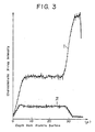
- the compound in the pores of the anodic oxide film was polymerized by heating. After the polymerization the A.C. dielectric strength between the anodic oxide film and the underlying base metal was determined, after which the sample in Example 2 was analyzed by means of an X-ray microanalyzer and it was noted that the micropores of the anodic oxide film was as shown in Fig. 3 impregnated with the organic compound to the innermost portion. Then the samples were subjected to heating at 300°C for 30 minutes except in Example 2, but neither cracking of the anodic oxide film nor degradation of electrical insulation thereof were noted. Further all the samples were allowed to stand in a room for a week, but no degradation of electrical insulation due to moisture in the air was noted.
- an anodic oxide film was formed on an aluminum or aluminum alloy plate and impregnated with polymerized organic compound as in Examples 1 to 4 under the conditions given in Tables 3A.
- the film thus formed was subjected to activation in an aqueous palladium chloride solution (0.5 g/1) at room temperature for 10 minutes, chemical nickel plating was carried out on the film to form a wiring conductor with a mask.
- the A.C. electric strength between the wiring conductor and the base metal was determined.
- Examples 10 and 11 the printed wiring boards thus obtained were heated up to 350°C for 20 minutes and with Example 7 up to 300°C for 30 minutes, but no cracking of the anodic oxide films was noted.
- every sample was allowed to stand in a room for one week, but no degradation of electric insulation was noted.
- An aluminum-silicon alloy plate containing 11% by weight of silicon and having through holes of minimum diameter 1 mm was prepared, the through holes each having a spherical portion.
- An anodic oxide film was formed on the aluminum-silicon alloy plate and impregnated with a polymerized organic compound as in Examples 1 to 4 under the conditions given in Table 3B. After the film was subjected to masking, it was immersed in an aqueous stannous chloride solution (10 g/I) for 30 seconds and then subjected to activation treatment in an aqueous palladium chloride solution (0.5 g/I) after washing with water. Thereafter the film was subjected to chemical nickel plating to form a wiring conductor thereon.
- dielectric strength between the circuit conductor and the underlying aluminum alloy plate was 400 V. Then the sample was subjected to heating at 300°C for 30 minutes but no cracking of the film was noted. Such were the case with the through holes. After the plate was allowed to stand in a room for a week, no degradation of electrical insulation was noted.
- An anodic oxide film was formed on the magnesium alloy plate (JIS-1) and impregnated with a polymerized organic compound as in Examples 1 to 4 under the conditions described in Table 3B. After the film thus formed was subjected to masking, it was immersed in an aqueous stannous chloride solution (5 g/I) for 30 seconds and then in an aqueous palladium chloride solution (0.5 g/l) for 30 seconds after washing. Thereafter the film was immersed in a shumer electroless nickel plating solution at 80°C for one minute to form a circuit thereon. A.C. dielectric strength between the circuit conductor and the base metal was 700 V or more.
- a heat radiant fin material made of extrudate of 6063 aluminum alloy having a cylindrical hole 7 of 25 mm diameter and 8 mm depth was prepared as shown in Fig. 4.
- the bottom of the hole was needed to be subjected to insulation treatment since this portion was to be in contact with an electric circuit.
- the material was subjected to anodization and then electrophoresis treatment after washing and drying under the conditions as given in Table 3B. After the fin material thus treated was wiped off and dried up at room temperature, it was heated up to 170°C for 2 hours for polymerization of the compound.
- An EC aluminum wire of 2 mm diameter was anodized by the well-known continuous line process including degreasing, first washing with water, anodization, second washing with water, and drying, the anodization being carried out under the conditions given in Table 3B.
- Table 3B An EC aluminum wire of 2 mm diameter was anodized by the well-known continuous line process including degreasing, first washing with water, anodization, second washing with water, and drying, the anodization being carried out under the conditions given in Table 3B.
- Table 3B Table 3B.
- the aluminum wire was subjected to impregnation by electrophoresis with an apparatus as shown in Fig. 5, in which a wire feeding drum 8 around which the aluminum wire was wound and a winding drum 9 were disposed on the opposite sides of a tank 10 containing a solution of 85 vol.% of methyltriethoxysilane, 10 vol.% of water and 5 vol.% of ethanol.
- the both ends of the aluminum wire were electrically connected to the metal bearings of the drums so that current flowed between the bearings. Then the wire was tightened and the center portion thereof was kept in the organic compound solution in the tank 10 by means of a pulley 11 for 5 minutes while the wire was being wound by the drum 9 with application of a D.C. voltage of 1000 V between a stainless electrode 12 disposed in the tank 10 and the aluminum wire. Before wound around the drum 9, the wire was wired up by a blower 13. The drum 9 was introduced into a thermoregulator (not shown) at 150°C for 2 hours for polymerization of the organic compound electrophoretically deposited on the anodic oxide film of the wire.
- test piece for each example in an electrolytic solution of which composition is given in Table 4.
- the test piece having an anodic oxide film thus formed thereon was immersed in an impregnating solution of which composition is described in the table and impregnated with a polymerizable organic compound contained in the solution by vacuum impregnate. After the test piece was taken up from the impregnating solution, the solution adhered to the surfaces thereof was removed by wiping off and then the test piece was dried up by exposing it to warm air except that in Examples 22 and 23 the test pieces were dried at room temperature. Thereafter the organic compound impregnated into the anodic oxide film was polymerized by heating. Dielectric strength between the film thus obtained and the underlying base metal was determined.
- test pieces were then heated up to 300°C for 30 minutes, but no cracking of the films was noted. Although the test pieces thus treated in Examples 20 and 23 were allowed to stand in a room for one week, no degradation of electric strength due to moisture was noted.
- a plate made of aluminum-silicon alloy containing 9% by weight of silicon was prepared.
- the plate had through holes each having a spherical portion and minimum diameter 1 mm.
- An anodic oxide film was under the conditions given in Table 4 formed on the plate and impregnated with an organic compound, which was then polymerized, as in Examples 18-25.
- the film thus formed was subjected to electroless nickel plating as in Example 14 to form a circuit conductor thereon.
- the A.C. electric strength between the circuit conductor and the underlying aluminum alloy plate was not less than 800 V. No cracking of the film was noted at a heating test af300°C for 30 minutes. Such were the case with the films of the through holes. No degradation of electric strength due to moisture was noted after it was allowed to stand in a room for one week.
- a sample plate was prepared as indicated under Example 26 using an aluminum-silicon alloy containing 11% by weight of silicon.
- An anodic oxide film impregnated with a polymerized organic compound was formed as in Examples 18-26 under the conditions described in Table 4.
- To obtain a printed wiring board the film was then subjected to chemical nickel plating as in Examples 7 to 13. It was found by means of X-ray microanalyzer that the micropores of the anodic oxide film was impregnated with the polymerized organic compound to the innermost portion.
- An anodic oxide film was under the conditions given in Table 5 formed on a test piece for each example by anodization, and subjected to impregnation treatment by applying impregnating solution containing a polymerizable organic compound to the film after which the organic compound impregnated into the film was polymerized by heating up to 130°C for 2 hours after drying the film to form a organic compound coating thereon of about 10 pm thickness.
- each film having a polymer layer thus formed thereon was subjected to chemical plating after activation as in Examples 7-13 to form a circuit conductor. Then the dielectric insulation between the circuit conductor and the parent metal of the printed wiring board was determined.
- Example 30 Although the wiring board was heated up to 350°C for 20 minutes, neither cracking nor degradation of electrical insulation of the anodic oxide film was noted. Also, no degradation of electrical insulation of the film due to moisture in the air was noted after the finished sample in each example was allowed to stand in a room for one week.
Landscapes
- Chemical & Material Sciences (AREA)
- Engineering & Computer Science (AREA)
- Chemical Kinetics & Catalysis (AREA)
- Electrochemistry (AREA)
- Materials Engineering (AREA)
- Metallurgy (AREA)
- Organic Chemistry (AREA)
- Inorganic Chemistry (AREA)
- Microelectronics & Electronic Packaging (AREA)
- Physics & Mathematics (AREA)
- Spectroscopy & Molecular Physics (AREA)
- General Chemical & Material Sciences (AREA)
- Insulated Metal Substrates For Printed Circuits (AREA)
Description
- This invention relates to a process for producing a treated anodic oxide film on a valve metal base, by anodizing the valve metal base to form thereon an anodic oxide film having micropores therein, applying a polymerisable compound thereto and polymerising the compound. The treated film has high heat radiance, heat resistance and electrical insulation. The invention also provides a method of making a printed wiring board using such anodic oxide film.
- Anodic oxide films formed on valve metals such as aluminium, titanium, magnesium, tantalum, and their alloys are electrically insulating metallic oxide films which are conversion-coated on their surfaces. The anodic oxide films have homogeneous composition and are excellent in adhesion to their base metal, corrosion resistance and thermal conductivity. By use of these properties metals having anodic oxide films formed thereon are widely used for printed wiring boards of electronic instruments, radiator plates of electronic parts, electrically insulative heat sinks, insulated wires, building materials and the like. In order to enhance insulation and corrosion properties thick anodic oxide films are used for such use, but for the oxide films having a thickness of not less than several microns a great number of micropores are necessarily formed therein. The micropores are very small holes having a diameter of several hundred angstroms which reach the barrier layer of the anodic oxide film. Entrance of moisture in the air into and residue of anodizing electrolytic solution in the micropores make it impossible to obtain a thick anodic oxide film having sufficiently high electrical insulation and corrosion resistance. To avoid these drawbacks sealing treatment can be rendered on the micropores for sealing thereof by the use of steam or boiling water. However by such treatment the anodic oxide film is subjected to hydration and cracks are produced in this hydrated film merely by heating it up to around 150°C.
- With respect to anodic oxide films subjected to no sealing treatment cracks occurtherein by heating up to about 200°C. The cracking is caused by thermal stresses in the anodic oxide film due to the difference in coefficient of thermal expansion between the film and its base metal. Cracked anodic oxide films are inferior in electrical insulation and corrosion resistance.
- For the sealing of the micropores there has been proposed another treatment that the micropores are impregnated with resins and the like. However micropores of almite films, for instance, have a very small diameter of several tens of nonometres and a depth of several ten micrometers and hence it in practice impossible to impregnate the micropores with resins to their innermost portions because of viscosity thereof.
- To solve this problem it has been proposed that electrodischarge is effected in an atmosphere of a gas of a compound such as organic silicon compound with an anodic oxide film made as one electrode, thereby depositing the compound in the micropores and on the surface of the oxide film. (Japanese Patent Publication (examined) or Koukoku Kouhou 49-4719). Since this treatment employs the electric discharge phenomenon, it is impossible to control the deposition position of the compound, so that it is difficult to sufficiently fill the micropores with the compound. Further the treatment has disadvantages that electric insulation property of the anodic oxide film is liable to be deteriorated due to moisture in the air since according to this treatment the compound cannot be compactly deposited and discharge current paths remain in the deposited compound.
- US-A-3 340 161 discloses the treatment of anodised aluminium, first with aqueous colloidal silica to deposit a thin silica film on top of the anodic oxide layer, and then with an organopolysiloxane solution, before drying and baking to cure the silicone' coating which seals the pores of the anodised film.
- The coated anodised aluminium substrate for an electrical printed circuit board which is resistant to high temperatures and is relatively inexpensive to produce.
- US-A-3 935 349 disclosed a method of coating an anodic oxide layer on aluminium which comprises treating the layer with a silane compound, applying a thermo-setting resin paint and then heat-curing the resin.
- This produces a coating on an anodised aluminium surface which adheres strongly to the anodic layer and which is highly resistant to mechanical and chemical attacks. As such the material produced is suitable for containers and constructive materials.
- It is an object of the present invention to provide a coated anodic oxide film with improved properties.
- According to the present invention there is provided a process for producing a treated anodic oxide film on a valve metal base, by anodizing the valve metal base to form thereon an anodic oxide film having micropores therein, dissolving in an organic solvent, water or a mixture thereof, a polymerisable compound applying the polymerisable compound to the anodic oxide film, polymerizing and hardening the compound and sealing the micropores of the anodic oxide film with the polymerised compound, characterised in that the polymerisable compound is represented by the formula:

- impregnating the anodic oxide film by vacuum impregnation or electrophoresis or electropermeation with the solution of the polymerisable compound to the innermost of the micropores; and
- polymerising and hardening the polymerisable compound impregnated into the anodic oxide film.
- Using this process, there is provided a base material having an anodic oxide film impregnated with polymerized compound which is excellent in heat radiance, heat resistance and electric insulation, and is hence useful for the printed wiring board, electrically insulative heat sink, heat-resistant insulated wire and the like.
- According to another aspect of the present invention, there is provided a method for making a printed wiring board having excellent heat radiance, heat resistance, and electric insulation. The printed wiring board comprises a base metal plate having an anodic oxide film formed thereon with micropores filled and sealed with an organometallic compound polymer material produced according to the process of the present invention, and a conductor circuit disposed on the compound polymer material. The above printed wiring board is produced according to a process which comprises the steps of: anodizing a base metal plate of a valve metal to form an anodic oxide film thereon; impregnating the anodic oxide film with a polymerizable compound, and polymerizing and hardening the polymerizable compound to form a compound polymer material thereby filling and sealing the micropores of the anodic oxide film, and thereafter disposing a conductor circuit on the polymer material.
-
- Fig. 1 is a diagrammatic cross section of a printed wiring board, produced according to the process of the present invention, having an alumite film formed thereon with micropores filled with an organometallic compound polymer;
- Fig. 2 is a diagrammatic cross section of a printed wiring board, produced according to the process of the present invention, having a compound polymer layer formed on an alumite surface thereof as well as the polymer deposit in its micropores,
- Fig. 3 is an experimental graph obtained by means of an X-ray microanalyzer and showing an organic compound polymer filled according to the present invention in micropores of an alumite film formed on an aluminum plate, in which graph I and II show distributions of AI and Si, respectively;
- Fig. 4 illustrates a perspective view of a heat sink material having fins which is processed according to the present invention; and
- Fig. 5 illustrates a diagrammatic view of an apparatus used in the present invention for treating electrophoretically an aluminum wire with a compound solution.
- The metals and their alloys employed as base metal in the present invention are anodizable valve metals such as aluminum, magnesium, titanium, tantalum, and their alloys.
- Aluminum or aluminum alloy base materials employed in the present invention include, for example, JIS-1 (A A1100) aluminum, high tensile aluminum alloy plate, corrosion-resistant aluminum alloy, and the like. Use may be made of aluminum-silicon alloy which contains not more than about 20% by weight, preferably about 5 to 15% by weight of silicon and if necessary a small amount of additives. The aluminum-silicon alloy has a property that its thermal expansion coefficient is in inverse proportion to silicon content in the alloy. For example, aluminum-silicon alloy containing 11 % by weight of silicon has a thermal expansion coefficient of 1.97xlO-', while aluminum and aluminum oxide have those of about 25x10-6 and about 6x10⁻⁶, respectively. This property provides a smaller difference in thermal expansion between aluminum-silicon alloy plate as base metal and an anodic oxide film formed thereon, so that the anodic oxide film formed on aluminum-silicon alloy plate has a less possibility of cracking and crazing than that of aluminum plate. The aluminum-silicon alloy contains silicon particles dispersed in an aluminum continuous phase and when anodized, the silicon particles remain in an anodic oxide film. The silicon particles serve to prevent or at least minimize the cracking of the anodic oxide film. Beyond about 20% by weight of silicon the insulating property of the anodic oxide film is largely degraded and is not acceptable for practical use.
- The magnesium material employed in the present invention may be any of those capable of forming an anodic oxide film including magnesium alloy such as the conventional ASTM AZ31C and AZ61A.
- In the case of producing a printed wiring board, a through hole, opening for attaching an electrical or electronic parts and the like may be previously formed in the base plate of valve metal.
- The base materials of the previously-mentioned metals or their alloys are anodized in an electrolytic bath such as sulphuric acid, oxalic acid and the like to form an anodic oxide film thereon. With base materials for a printed wiring board, an anodic oxide film having a thickness of about 5 to about 200 µm is formed.
- Anodizing treatment of base materials of aluminum or aluminum alloy is carried out in an electrolytic bath containing, for example, an ammonium salt such as ammonium tartrate, ammonium hydroxide, ammonium carbonate, and ammonium fluoride, or a sodium salt such as sodium hydroxide, and sodium pyrophosphate. The ammonium ion concentration in the electrolytic bath may be within a range of about 5 to about 80 g/I, and preferably about 5 to 40 g/I. The sodium ion concentration in the electrolytic bath may be within a range of about 1 to 30 g/l, and preferably about 1 to about 20 g/I. The bath temperature may be within a range of about 5 to 40°C, and current density may be of about 0.5 to 10 AJdm2. In anodic oxide films obtained on the basis of the above-mentioned electrolytic bath and electrolysis conditions, temperatures above which cracking of the films occurs are raised, and heat resistance of the films is enhanced.
- Alternatively, the anodizing treatment may be carried out by the use of about 4 to about 25% by weight, preferably about 7 to about 20% by weight, of aqueous oxalic acid solution as an electrolytic bath under the conditions of a bath temperature of about 20 to 50°C and a current density of about 0.5 to 10 A/dm2, preferably 1.5 to 5 A/dm2 with an aluminum plate or aluminum alloy plate being made the anode and a suitable inert conductor such as stainless steel piece the cathode. By restricting anodizing conditions to within the above outer limitations cracking temperature of the alumite film thus formed can be raised, and hence heat resistance of the film is improved. The results of comparative tests showing this fact are given in Tables 1 and 2.
- The process of forming an anodic oxide film on the magnesium base material used in the present invention may be any one of the conventional treatments such as HAE (U.S. Patent 2,880,148, ASTM Class II Type III), Dow Anodizing (ASTM Class II type II) and the like. (See for example "Kinzoku Hyomen Gijutsu Binran" published by Nikkan Kogyo Shinbunsha, Japan, 1976, pp. 710-711).
- Thus-formed anodic oxide film is impregnated with a polymerizable compound. Before this impregnation, if needed, the anodic oxide film may be subjected to the well-known sealing treatment by the use of steam, boiling water, and the like.
- The polymerizable compounds used in the present invention include, for example, organosilicon compounds such as phenyltriethoxysilane, methyltriethoxysilane, vinyltris((3-methoxyethoxy) siiane, P - (3,4 - epoxy - cyclohexyl)ethyltrimethoxysilane, and y-glycideoxypropyltrimethoxysilane; organotitanium compounds; organoalumirium compounds; organozirconium compounds; organic phosphate compounds; organoboron compounds; organogermanium compounds such as dimethyloxydimethyl germanium, and methylgermanium trimethoxide; dimethyloxyethyl tin; and their derivatives and oligomers. The polymerizable compounds employed in the present invention preferably contain Si, Al, Zr or Ti as M. Further the compound contains preferably methyl and/or phenyl group as an organic group for improving heat resistance of the anodic oxide film. The organic compound of which hydrolysis takes place gradually is preferred in the present invention. The above-mentioned polymerizable organic compounds are used in the form of a solution in organic solvent such as methanol, ethanol, acetone, ethyl acetate, and methyl ethyl ketone; water; or mixture of water and a water soluble organic solvent. Such soluble organic solvent may include methanol, ethanol, isopropanol, acetone, dioxane, ethylene glycol, methyl acetate, methyl ethyl ketone, diacetone alcohol, ethyl formate, dimethylformamide, and the like. An additive such as surfactant may be added to the soluble organic solvent, if needed.
- In an embodiment of the invention the impregnation with the polymerizable organic compound is carried out by vacuum impregnate treatment. Alternatively, the impregnation is achieved by electrophoresis or electropermeation in which an anodic oxide film is immersed in a solution of the polymerizable organic compound in water or a mixture of water and a water soluble organic solvent, and then direct current is applied between the anodic oxide film as the anode and a suitable inert conductor such as stainless steel piece as the cathode so that the micropores of the film are fully impregnated with the organic compound from their bottom to open end. After impregnation of the anodic oxide film with the polymerizable organic compound, the solution of the organic compound adhered to the surface of the film is sufficiently wiped off to provide a high thermal conductivity or is remained without wiping to provide a high electrical insulation. The anodic oxide film is dried up to remove the water and the organic solvent in the solution after the polymerizable organic compound is fully adhered to and deposited in the micropores or on the surface of the film.
- Finally, the organic compound thus deposited is polymerized by conventional treatment such as heating, so that a compact organic compound polymer material is obtained. The organic compound polymer has high affinity to the anodic oxide film, and hence it strongly adheres to the walls of the micropores or the surface of the film, and fills compactly the micropores or positively cover the surface.
- The anodic oxide film subjected to the sealing treatment with an organic compound according to the present invention has micropores compactly filled with the organic compound polymer and may have a surface covered with the polymer, and thus very high electric insulation is given to the anodic oxide film. The organic compound polymer material can be deposited only in the micropores of the anodic oxide film by previously wiping off the solution of the organic compound sticked to the surface of the film. Also in this case the film has sufficient electrical insulation of the film even up to about 150°C as well as excellent thermal conductivity. The anodic oxide film covered with the defined organic compound polymer which is excellent in thermal conductivity has much higher thermal conductivity than those covered with any other conventional resins.
- The thus prepared base plate on which a wiring conductor can be mounted may be used as a printed wiring board having excellent heat resistance, electrical insulation and heat radiance.
- In order to manufacture such a printed wiring board, an anodic oxide film is formed on a base plate of a valve metal having a recess for attaching a part, through holes, etc. previously formed therein, and then the film is impregnated with the polymerizable organic compound by diffusion, vacuum impregnate, electrophoresis and the like as previously described.
- By such treatment the through holes and part-attaching recess of the printed wiring board are insulated without any difficulty. Anodizing treatment which has a good throwing power can form an anodic oxide film of a uniform thickness on the wall surfaces of the recess. This is because thick grown portion of the anodic oxide film has a larger resistance which causes the current to flow through a thin portion of the film which has a lower resistance with a tendency to make the thickness of the film uniform. Also in the impregnation with an organic compound by electrophoresis resistance gradually increases and current becomes less easy to flow with the progress of the impregnation and thus current flows sufficiently through a portion relatively difficult to be impregnated, so that the impregnation is carried out uniformly and even the wall of the part-attaching recess and the like can be sufficiently impregnated with the organic compound.
- Then, the anodic oxide film impregnated with the polymerizable organic compound is subjected to heating or photopolymerization treatment to polymerize the compound. A circuit conductor is formed on or in the anodic oxide film thus impregnated with an organic compound polymer. This formation of the circuit conductor is carried out by either directly forming a circuit in the film by means of a well-known method such as electroless plating, vacuum evaporation, ion sputtering, and ion plating or adhering to the film a film of copper, nickel or the like which is then subjected to etching to form a desired wiring circuit of a thickness about several ten microns. The copper or nickel film as a conductor may be attached to the anodic oxide film through the polymerizable organic compound applied on the film in place of adhesive and thereafter the organic compound is polymerized to form a printed wiring board with the conductor fixedly attached to the film.
- Two embodiments of the printed wiring board thus obtained according to the present invention are illustrated in Figs. 1 and 2, in which an aluminum plate is used as an anodizable metal plate. In Fig. 1, the
micropores 3 of analumite film 2 formed on the aluminum plate are filled with anorganic compound polymer 4 and awiring conductor 5 is formed directly on the outer surface of thealumite film 2. In Fig. 2, ancompound polymer layer 6 is further formed between thealumite film 2 and thewiring conductor 5. - The anodic oxide film of a printed wiring board treated with a polymerizable organic compound according to the present invention has micropores compactly filled with an organic compound polymer or a surface covered with the latter as well as its through hole and hence has very high electrical insulation. The organic compound polymer can be deposited only in the micropores, which results in improvement of electrical insulation as well as high thermal conductivity. Furthermore, its electrical insulation at high temperatures (about 150°C) is enhanced. In addition the anodic oxide film filled and covered with the polymer which is excellent in thermal conductivity has much higher thermal conductivity and heat radiance than that covered with any other conventional resins.
- When an aluminum-silicon alloy is used as a base metal, the difference in thermal expansion coefficient between the base metal and an anodic film formed thereon becomes smaller, so that cracking of the film is prevented or at least minimized when heated and electrical insulation thereof at high temperatures is improved.
- In order to prevent more positively heat cracking of an anodic oxide film impregnated with a polymerized organic compound, it is recommended that cracks are previously generated in the anodic oxide film by heating, and then the micropores and cracks of the oxide film are impregnated with the polymerizable organic compound, which is thereafter polymerized. In the anodic oxide film thus formed there will be no cracking by heating up to the temperature of the heat treatment.
- To improve further heat radiance, corrosion resistance and electrical insulation of the printed wiring board, it is preferred to use an aluminum plate cladded with the other metal plate as a base plate.
- Six sample plates of AA1100 aluminum (hereinafter referred to as 2S aluminum) and 50 mm x 100 mmx1 mm in dimensions were prepared and anodized in 10% by weight of aqueous oxalic acid solution under the temperature and current density conditions described in Table 1 to a film thickness of 30 u. The sample plates having anodic oxide films thus formed were each heated up to a temperature at which cracking of the film was noted. The cracking temperatures are shown in the following table.

- The results show that an anodic oxide film formed by anodizing at 20°C or more using a current density of 1.5 Aldm2 or more will crack at not less than 400°C, and is excellent in heat resistance.
- Twenty one sample plates of 2S aluminum having dimensions of 50 mmx100 mmx1 mm were prepared and anodized in specific concentrations of aqueous oxalic acid solution using a current density of 2 A/dm2 to a film thickness of 30 p. The anodization was carried out at 30°C, 42°C, and 50°C for 3 to 15, 20, and 25% by weight of oxalic acid solution, respectively. The sample plates were then heated and judgement as to whether or not cracking of the anodic oxide film occurs were made on each sample plate. The results are shown in Table 2.

- For each example a test piece of aluminum or aluminum alloy was introduced into an acid bath or ammonium bath of which composition is given in Table 3A and anodization was carried out under the specific conditions to form an anodic oxide film on the test piece. Then, the test piece was immersed in an impregnating solution containing a polymerizable organic compound as shown in the table, where electrophoresis or electropermeation of the organic compound was carried out by making the anodic oxide film thus formed the anode with application of a predetermined direct current voltage for a predetermined period of time. After the test piece was taken up from the impregnating solution, the solution adhered to the surfaces thereof was either removed sufficiently by wiping off or remained, and then the test piece was dried up by exposing it to warm air. Thereafter the compound in the pores of the anodic oxide film was polymerized by heating. After the polymerization the A.C. dielectric strength between the anodic oxide film and the underlying base metal was determined, after which the sample in Example 2 was analyzed by means of an X-ray microanalyzer and it was noted that the micropores of the anodic oxide film was as shown in Fig. 3 impregnated with the organic compound to the innermost portion. Then the samples were subjected to heating at 300°C for 30 minutes except in Example 2, but neither cracking of the anodic oxide film nor degradation of electrical insulation thereof were noted. Further all the samples were allowed to stand in a room for a week, but no degradation of electrical insulation due to moisture in the air was noted.
- For each example an anodic oxide film was formed on an aluminum or aluminum alloy plate and impregnated with polymerized organic compound as in Examples 1 to 4 under the conditions given in Tables 3A. After the film thus formed was subjected to activation in an aqueous palladium chloride solution (0.5 g/1) at room temperature for 10 minutes, chemical nickel plating was carried out on the film to form a wiring conductor with a mask. The A.C. electric strength between the wiring conductor and the base metal was determined. With Examples 10 and 11 the printed wiring boards thus obtained were heated up to 350°C for 20 minutes and with Example 7 up to 300°C for 30 minutes, but no cracking of the anodic oxide films was noted. In addition every sample was allowed to stand in a room for one week, but no degradation of electric insulation was noted.


- An aluminum-silicon alloy plate containing 11% by weight of silicon and having through holes of minimum diameter 1 mm was prepared, the through holes each having a spherical portion. An anodic oxide film was formed on the aluminum-silicon alloy plate and impregnated with a polymerized organic compound as in Examples 1 to 4 under the conditions given in Table 3B. After the film was subjected to masking, it was immersed in an aqueous stannous chloride solution (10 g/I) for 30 seconds and then subjected to activation treatment in an aqueous palladium chloride solution (0.5 g/I) after washing with water. Thereafter the film was subjected to chemical nickel plating to form a wiring conductor thereon. A.C. dielectric strength between the circuit conductor and the underlying aluminum alloy plate was 400 V. Then the sample was subjected to heating at 300°C for 30 minutes but no cracking of the film was noted. Such were the case with the through holes. After the plate was allowed to stand in a room for a week, no degradation of electrical insulation was noted.
- An anodic oxide film was formed on the magnesium alloy plate (JIS-1) and impregnated with a polymerized organic compound as in Examples 1 to 4 under the conditions described in Table 3B. After the film thus formed was subjected to masking, it was immersed in an aqueous stannous chloride solution (5 g/I) for 30 seconds and then in an aqueous palladium chloride solution (0.5 g/l) for 30 seconds after washing. Thereafter the film was immersed in a shumer electroless nickel plating solution at 80°C for one minute to form a circuit thereon. A.C. dielectric strength between the circuit conductor and the base metal was 700 V or more.
- A heat radiant fin material made of extrudate of 6063 aluminum alloy having a
cylindrical hole 7 of 25 mm diameter and 8 mm depth was prepared as shown in Fig. 4. The bottom of the hole was needed to be subjected to insulation treatment since this portion was to be in contact with an electric circuit. The material was subjected to anodization and then electrophoresis treatment after washing and drying under the conditions as given in Table 3B. After the fin material thus treated was wiped off and dried up at room temperature, it was heated up to 170°C for 2 hours for polymerization of the compound. - An EC aluminum wire of 2 mm diameter was anodized by the well-known continuous line process including degreasing, first washing with water, anodization, second washing with water, and drying, the anodization being carried out under the conditions given in Table 3B. To obtain about 10 kg of the aluminum wire having an anodic oxide film of 10 p thickness. Subsequently, the aluminum wire was subjected to impregnation by electrophoresis with an apparatus as shown in Fig. 5, in which a
wire feeding drum 8 around which the aluminum wire was wound and a winding drum 9 were disposed on the opposite sides of atank 10 containing a solution of 85 vol.% of methyltriethoxysilane, 10 vol.% of water and 5 vol.% of ethanol. The both ends of the aluminum wire were electrically connected to the metal bearings of the drums so that current flowed between the bearings. Then the wire was tightened and the center portion thereof was kept in the organic compound solution in thetank 10 by means of a pulley 11 for 5 minutes while the wire was being wound by the drum 9 with application of a D.C. voltage of 1000 V between a stainless electrode 12 disposed in thetank 10 and the aluminum wire. Before wound around the drum 9, the wire was wired up by ablower 13. The drum 9 was introduced into a thermoregulator (not shown) at 150°C for 2 hours for polymerization of the organic compound electrophoretically deposited on the anodic oxide film of the wire.
- Anodization was carried out on a test piece for each example in an electrolytic solution of which composition is given in Table 4. The test piece having an anodic oxide film thus formed thereon was immersed in an impregnating solution of which composition is described in the table and impregnated with a polymerizable organic compound contained in the solution by vacuum impregnate. After the test piece was taken up from the impregnating solution, the solution adhered to the surfaces thereof was removed by wiping off and then the test piece was dried up by exposing it to warm air except that in Examples 22 and 23 the test pieces were dried at room temperature. Thereafter the organic compound impregnated into the anodic oxide film was polymerized by heating. Dielectric strength between the film thus obtained and the underlying base metal was determined. With respect to Examples 18, 19, and 20 the test pieces were then heated up to 300°C for 30 minutes, but no cracking of the films was noted. Although the test pieces thus treated in Examples 20 and 23 were allowed to stand in a room for one week, no degradation of electric strength due to moisture was noted.
- A plate made of aluminum-silicon alloy containing 9% by weight of silicon was prepared. The plate had through holes each having a spherical portion and minimum diameter 1 mm. An anodic oxide film was under the conditions given in Table 4 formed on the plate and impregnated with an organic compound, which was then polymerized, as in Examples 18-25. The film thus formed was subjected to electroless nickel plating as in Example 14 to form a circuit conductor thereon. The A.C. electric strength between the circuit conductor and the underlying aluminum alloy plate was not less than 800 V. No cracking of the film was noted at a heating test af300°C for 30 minutes. Such were the case with the films of the through holes. No degradation of electric strength due to moisture was noted after it was allowed to stand in a room for one week.
- A sample plate was prepared as indicated under Example 26 using an aluminum-silicon alloy containing 11% by weight of silicon. An anodic oxide film impregnated with a polymerized organic compound was formed as in Examples 18-26 under the conditions described in Table 4. To obtain a printed wiring board the film was then subjected to chemical nickel plating as in Examples 7 to 13. It was found by means of X-ray microanalyzer that the micropores of the anodic oxide film was impregnated with the polymerized organic compound to the innermost portion.
- Five 2S aluminum plates were prepared and subjected to anodization and vacuum impregnate as in Examples 18-27 under the conditions given in Table 4, after which they were subjected to hydrolysis by allowing them to stand in the air for 24 hours and then heated up to 130°C for 2 hours for polymerization of the organic compound. Then the plates were subjected to masking, and cut into fifteen test pieces of 10x10x1 mm3 in dimensions which were in turn subjected to electroless plating as in Example 15.


- An anodic oxide film was under the conditions given in Table 5 formed on a test piece for each example by anodization, and subjected to impregnation treatment by applying impregnating solution containing a polymerizable organic compound to the film after which the organic compound impregnated into the film was polymerized by heating up to 130°C for 2 hours after drying the film to form a organic compound coating thereon of about 10 pm thickness. With respect to Examples 30 and 31 each film having a polymer layer thus formed thereon was subjected to chemical plating after activation as in Examples 7-13 to form a circuit conductor. Then the dielectric insulation between the circuit conductor and the parent metal of the printed wiring board was determined. With respect to Example 30, although the wiring board was heated up to 350°C for 20 minutes, neither cracking nor degradation of electrical insulation of the anodic oxide film was noted. Also, no degradation of electrical insulation of the film due to moisture in the air was noted after the finished sample in each example was allowed to stand in a room for one week.

- An anodic oxide film was formed on a 100 mmx50 mm x mm 2S aluminum plate as in Example 29. Then, the test piece was immersed and allowed to stay in an ethanol solution of CH2=CHSi(OCZH40CH3)3 (20 vol.%) for one hour, so that the solution permeated or diffused into the micropores of the anodic oxide film. After the test piece was taken up from the ethanol solution, the solution adhered to the surfaces thereof was removed by wiping, the organic compound which diffused into the anodic oxide film was subjected to polymerization treatment by heating at 150°C for two hours. The insulating voltage of the anodic oxide film was 500 V or more.
- Twelve sample plates of 2S aluminum having dimensions of 50 mmx100 mmx1 mm were prepared and anodized in an ammonium tartrate solution under the temperature and current density conditions described in Table 6 to a film thickness of 10 u. The sample plates having anodic oxide films thus formed were each heated up to a temperature at which cracking of the film was noted. The cracking temperature are shown in the following table.

- As apparent from the table, within wide ranges of the bath temperature and current density there was noted no cracking of the anodic oxide films up to around 400°C, and the films were excellent in heat resistance.
Claims (15)

Applications Claiming Priority (10)
| Application Number | Priority Date | Filing Date | Title |
|---|---|---|---|
| JP1394681A JPS5853718B2 (en) | 1981-02-02 | 1981-02-02 | How to treat anodized film |
| JP13945/81 | 1981-02-02 | ||
| JP1394381A JPS5922396B2 (en) | 1981-02-02 | 1981-02-02 | Printed wiring board manufacturing method |
| JP13942/81 | 1981-02-02 | ||
| JP1394581A JPS5853719B2 (en) | 1981-02-02 | 1981-02-02 | How to treat anodized film |
| JP13946/81 | 1981-02-02 | ||
| JP1394281A JPS5922395B2 (en) | 1981-02-02 | 1981-02-02 | Printed wiring board manufacturing method |
| JP13943/81 | 1981-02-02 | ||
| JP3497481A JPS5853720B2 (en) | 1981-03-11 | 1981-03-11 | How to treat anodized film |
| JP34974/81 | 1981-03-11 |
Publications (3)
| Publication Number | Publication Date |
|---|---|
| EP0058023A2 EP0058023A2 (en) | 1982-08-18 |
| EP0058023A3 EP0058023A3 (en) | 1982-08-25 |
| EP0058023B1 true EP0058023B1 (en) | 1986-05-07 |
Family
ID=27519572
Family Applications (1)
| Application Number | Title | Priority Date | Filing Date |
|---|---|---|---|
| EP82300465A Expired EP0058023B1 (en) | 1981-02-02 | 1982-01-29 | Process of treating anodic oxide film, printed wiring board and process of making the same |
Country Status (4)
| Country | Link |
|---|---|
| US (1) | US4483751A (en) |
| EP (1) | EP0058023B1 (en) |
| CA (1) | CA1212073A (en) |
| DE (1) | DE3270926D1 (en) |
Families Citing this family (36)
| Publication number | Priority date | Publication date | Assignee | Title |
|---|---|---|---|---|
| GB2111312A (en) * | 1981-11-04 | 1983-06-29 | Philips Electronic Associated | Substrates for electrical circuits |
| IT1228581B (en) * | 1982-06-29 | 1991-06-24 | Italtecno Srl | Sealing anodically oxidised aluminium and alloys - with solns. contg. hydroxylated organic cpd. to improve resistance to alkali |
| EP0196865B1 (en) * | 1985-03-27 | 1990-09-12 | Ibiden Co, Ltd. | Electronic circuit substrates |
| DE3517796A1 (en) * | 1985-05-17 | 1986-11-20 | Hoechst Ag, 6230 Frankfurt | METHOD FOR PRODUCING ELECTRICALLY INSULATING BASE MATERIAL FOR THE PRODUCTION OF CONTACTED CIRCUIT BOARDS |
| GB8531445D0 (en) * | 1985-12-20 | 1986-02-05 | Gen Electric Co Plc | Thin films |
| DE3626232A1 (en) * | 1986-08-02 | 1988-03-10 | Akyuerek Susanne | Process for producing a printed circuit board |
| EP0366338A3 (en) * | 1988-10-26 | 1990-11-22 | Texas Instruments Incorporated | A substrate for an electrical circuit system and a circuit system using that substrate |
| EP0410003B1 (en) * | 1989-02-14 | 1994-11-02 | Sumitomo Electric Industries, Ltd. | Insulated electric wire |
| JPH051347A (en) * | 1991-06-21 | 1993-01-08 | Furukawa Alum Co Ltd | Lightweight V-groove pulley |
| GB9321502D0 (en) * | 1993-10-19 | 1993-12-08 | Dow Corning Sa | Electrical testing process and method of sealing using same |
| US6410144B2 (en) | 1995-03-08 | 2002-06-25 | Southwest Research Institute | Lubricious diamond-like carbon coatings |
| WO1996027699A1 (en) * | 1995-03-08 | 1996-09-12 | Southwest Research Institute | A non-chromate sealant for porous anodized aluminum |
| US6042896A (en) * | 1995-03-08 | 2000-03-28 | Southwest Research Institute | Preventing radioactive contamination of porous surfaces |
| FR2763780B1 (en) * | 1997-05-20 | 1999-08-13 | Sagem | METHOD FOR MANUFACTURING PRINTED CIRCUITS ON A METAL SUBSTRATE |
| DE19741580A1 (en) * | 1997-09-20 | 1999-04-01 | Bosch Gmbh Robert | Composite |
| US6410197B1 (en) * | 1998-09-18 | 2002-06-25 | Lexmark International, Inc. | Methods for treating aluminum substrates and products thereof |
| JP2001156321A (en) * | 1999-03-09 | 2001-06-08 | Fuji Xerox Co Ltd | Semiconductor device and method of manufacturing the same |
| US6312565B1 (en) * | 2000-03-23 | 2001-11-06 | Agere Systems Guardian Corp. | Thin film deposition of mixed metal oxides |
| US20080067073A1 (en) * | 2004-07-06 | 2008-03-20 | Kenichi Kagawa | Interposer And Manufacturing Method For The Same |
| US20100255274A1 (en) * | 2007-05-24 | 2010-10-07 | Uri Mirsky | Deep anodization |
| DE212014000273U1 (en) | 2014-08-29 | 2017-04-26 | Apple Inc. | Process for reducing the spallation of anodic oxide layers of high strength substrate alloys |
| US9842971B2 (en) * | 2014-09-24 | 2017-12-12 | Kyocera Corporation | Electronic component mounting substrate and light emission device using same |
| US9359686B1 (en) | 2015-01-09 | 2016-06-07 | Apple Inc. | Processes to reduce interfacial enrichment of alloying elements under anodic oxide films and improve anodized appearance of heat treatable alloys |
| CN104788127B (en) * | 2015-03-31 | 2017-03-29 | 深圳顺络电子股份有限公司 | Electronic ceramic component is suppressed to climb the surface treatment method and electronic ceramic component of plating |
| WO2016160036A1 (en) | 2015-04-03 | 2016-10-06 | Apple Inc. | Process for evaluation of delamination-resistance of hard coatings on metal substrates |
| US10760176B2 (en) | 2015-07-09 | 2020-09-01 | Apple Inc. | Process for reducing nickel leach rates for nickel acetate sealed anodic oxide coatings |
| JP6829961B2 (en) * | 2015-08-13 | 2021-02-17 | 株式会社Uacj | Surface-treated aluminum material with excellent resin adhesion and its manufacturing method, and surface-treated aluminum material / resin joint |
| US9970080B2 (en) | 2015-09-24 | 2018-05-15 | Apple Inc. | Micro-alloying to mitigate the slight discoloration resulting from entrained metal in anodized aluminum surface finishes |
| US10711363B2 (en) | 2015-09-24 | 2020-07-14 | Apple Inc. | Anodic oxide based composite coatings of augmented thermal expansivity to eliminate thermally induced crazing |
| CN105632672B (en) * | 2015-12-30 | 2017-12-01 | 深圳顺络电子股份有限公司 | A kind of electronic ceramic component surface treatment method and surface treatment liquid |
| US10174436B2 (en) | 2016-04-06 | 2019-01-08 | Apple Inc. | Process for enhanced corrosion protection of anodized aluminum |
| US11352708B2 (en) | 2016-08-10 | 2022-06-07 | Apple Inc. | Colored multilayer oxide coatings |
| US11242614B2 (en) | 2017-02-17 | 2022-02-08 | Apple Inc. | Oxide coatings for providing corrosion resistance on parts with edges and convex features |
| US11549191B2 (en) | 2018-09-10 | 2023-01-10 | Apple Inc. | Corrosion resistance for anodized parts having convex surface features |
| EP3749054A1 (en) | 2019-06-03 | 2020-12-09 | Patentbox Internacional, S.L. | Arrangement of elements in an electric heating plate and its manufacturing procedure |
| EP4361320A1 (en) * | 2022-10-24 | 2024-05-01 | Gramm Technik GmbH | Electrochemical substitution under vacuum of oxide layers on light metals |
Family Cites Families (11)
| Publication number | Priority date | Publication date | Assignee | Title |
|---|---|---|---|---|
| GB877736A (en) * | 1959-02-13 | 1961-09-20 | Ici Ltd | Improvements in or relating to anodised aluminium and aluminium alloy articles and their productions |
| US3202591A (en) * | 1961-11-24 | 1965-08-24 | Electralab Printed Electronics | Method of making an electric circuit structure |
| US3340161A (en) * | 1964-02-19 | 1967-09-05 | Sperry Rand Corp | Printed circuits and method of manufacture thereof |
| US3622473A (en) * | 1964-10-15 | 1971-11-23 | Honny Chemicals Co Ltd | Method of providing aluminum surfaces with coatings |
| US3711313A (en) * | 1969-09-06 | 1973-01-16 | Riken Light Metal Ind Co | Process for the deposition of resinous films on aluminum-bearing substrates |
| US3715211A (en) * | 1971-02-01 | 1973-02-06 | Horizons Inc | Process and product of cold sealing an anodized aluminum article by a photo-polymerization process |
| JPS5124292B2 (en) * | 1972-10-06 | 1976-07-23 | ||
| US4084021A (en) * | 1974-10-08 | 1978-04-11 | Minnesota Mining And Manufacturing Company | Method for rendering substrates resistant to abrasion |
| US4130466A (en) * | 1978-05-31 | 1978-12-19 | The United States Of America As Represented By The Secretary Of The Navy | Antifouling coating for aluminum structures |
| US4180442A (en) * | 1978-06-14 | 1979-12-25 | Mcdonnell Douglas Corporation | Electrodeposition of coatings on metals to enhance adhesive bonding |
| US4318939A (en) * | 1980-08-21 | 1982-03-09 | Western Electric Co., Incorporated | Stabilized catalyzed organopolysiloxanes |
-
1982
- 1982-01-28 CA CA000395127A patent/CA1212073A/en not_active Expired
- 1982-01-29 DE DE8282300465T patent/DE3270926D1/en not_active Expired
- 1982-01-29 EP EP82300465A patent/EP0058023B1/en not_active Expired
- 1982-02-01 US US06/344,711 patent/US4483751A/en not_active Expired - Lifetime
Also Published As
| Publication number | Publication date |
|---|---|
| DE3270926D1 (en) | 1986-06-12 |
| EP0058023A2 (en) | 1982-08-18 |
| US4483751A (en) | 1984-11-20 |
| EP0058023A3 (en) | 1982-08-25 |
| CA1212073A (en) | 1986-09-30 |
Similar Documents
| Publication | Publication Date | Title |
|---|---|---|
| US4483751A (en) | Process of treating a nodic oxide film, printed wiring board and process of making the same | |
| US3704176A (en) | Method of resin coating a metal and resin-coated metal product thereof | |
| EP0405624B1 (en) | Method for anodizing aluminium | |
| EP0177686B1 (en) | Process for bonding metals to electrophoretically deposited coatings, and printed circuit with plated through holes produced thereby | |
| JPH06192887A (en) | Protective covering for metal part for use at high temperature | |
| CN101031674A (en) | Method for anticorrosion-treating aluminum or aluminum alloy | |
| CN103029247A (en) | Electrical insulating cast article and manufacturing method thereof | |
| KR19990023387A (en) | How to increase the adhesion of metal foil | |
| JP2024111338A (en) | Aluminum-based member and manufacturing method thereof | |
| JP2000203970A (en) | Treatment of porous surface, porous surface treating agent, surface-treated body and polymerization accelerator | |
| RU2068037C1 (en) | Method to produce composition coatings on aluminum and its alloys | |
| JPS5922395B2 (en) | Printed wiring board manufacturing method | |
| JPS64838B2 (en) | ||
| JPH11229187A (en) | Substrate for electronic material excellent in insulation and method of manufacturing the same | |
| JP2003073853A (en) | Surface-treated aluminum material having excellent corrosion resistance and method for producing the same | |
| US4714646A (en) | Electrophoretic insulation of metal circuit board core | |
| JPS5834558B2 (en) | Treatment method for anodic oxide film | |
| JPS5922396B2 (en) | Printed wiring board manufacturing method | |
| JPS5853719B2 (en) | How to treat anodized film | |
| JPS5853718B2 (en) | How to treat anodized film | |
| JPS5853720B2 (en) | How to treat anodized film | |
| JP2614233B2 (en) | Manufacturing method of electrostatic recording medium | |
| SU1715890A1 (en) | Method of producing heat resistance coats on aluminum alloys | |
| EP0239839B1 (en) | Electrophoretic insulation of metal circuit board core | |
| JPS5834556B2 (en) | How to treat anodized film |
Legal Events
| Date | Code | Title | Description |
|---|---|---|---|
| PUAI | Public reference made under article 153(3) epc to a published international application that has entered the european phase |
Free format text: ORIGINAL CODE: 0009012 |
|
| PUAL | Search report despatched |
Free format text: ORIGINAL CODE: 0009013 |
|
| AK | Designated contracting states |
Designated state(s): CH DE FR GB IT |
|
| AK | Designated contracting states |
Designated state(s): CH DE FR GB IT |
|
| 17P | Request for examination filed |
Effective date: 19820928 |
|
| GRAA | (expected) grant |
Free format text: ORIGINAL CODE: 0009210 |
|
| ITF | It: translation for a ep patent filed | ||
| AK | Designated contracting states |
Kind code of ref document: B1 Designated state(s): CH DE FR GB IT LI |
|
| REF | Corresponds to: |
Ref document number: 3270926 Country of ref document: DE Date of ref document: 19860612 |
|
| ET | Fr: translation filed | ||
| PLBE | No opposition filed within time limit |
Free format text: ORIGINAL CODE: 0009261 |
|
| STAA | Information on the status of an ep patent application or granted ep patent |
Free format text: STATUS: NO OPPOSITION FILED WITHIN TIME LIMIT |
|
| 26N | No opposition filed | ||
| ITTA | It: last paid annual fee | ||
| PGFP | Annual fee paid to national office [announced via postgrant information from national office to epo] |
Ref country code: FR Payment date: 19970109 Year of fee payment: 16 |
|
| PGFP | Annual fee paid to national office [announced via postgrant information from national office to epo] |
Ref country code: GB Payment date: 19970120 Year of fee payment: 16 |
|
| PGFP | Annual fee paid to national office [announced via postgrant information from national office to epo] |
Ref country code: CH Payment date: 19970206 Year of fee payment: 16 |
|
| PGFP | Annual fee paid to national office [announced via postgrant information from national office to epo] |
Ref country code: DE Payment date: 19970207 Year of fee payment: 16 |
|
| PG25 | Lapsed in a contracting state [announced via postgrant information from national office to epo] |
Ref country code: GB Free format text: LAPSE BECAUSE OF NON-PAYMENT OF DUE FEES Effective date: 19980129 |
|
| PG25 | Lapsed in a contracting state [announced via postgrant information from national office to epo] |
Ref country code: LI Free format text: LAPSE BECAUSE OF NON-PAYMENT OF DUE FEES Effective date: 19980131 Ref country code: FR Free format text: THE PATENT HAS BEEN ANNULLED BY A DECISION OF A NATIONAL AUTHORITY Effective date: 19980131 Ref country code: CH Free format text: LAPSE BECAUSE OF NON-PAYMENT OF DUE FEES Effective date: 19980131 |
|
| REG | Reference to a national code |
Ref country code: CH Ref legal event code: PL |
|
| GBPC | Gb: european patent ceased through non-payment of renewal fee |
Effective date: 19980129 |
|
| PG25 | Lapsed in a contracting state [announced via postgrant information from national office to epo] |
Ref country code: DE Free format text: LAPSE BECAUSE OF NON-PAYMENT OF DUE FEES Effective date: 19981001 |
|
| REG | Reference to a national code |
Ref country code: FR Ref legal event code: ST |