EP0057515A2 - Signalgeneratoren - Google Patents
Signalgeneratoren Download PDFInfo
- Publication number
- EP0057515A2 EP0057515A2 EP82300166A EP82300166A EP0057515A2 EP 0057515 A2 EP0057515 A2 EP 0057515A2 EP 82300166 A EP82300166 A EP 82300166A EP 82300166 A EP82300166 A EP 82300166A EP 0057515 A2 EP0057515 A2 EP 0057515A2
- Authority
- EP
- European Patent Office
- Prior art keywords
- control
- output
- data
- conbus
- lines
- Prior art date
- Legal status (The legal status is an assumption and is not a legal conclusion. Google has not performed a legal analysis and makes no representation as to the accuracy of the status listed.)
- Withdrawn
Links
Images

Classifications
-
- G—PHYSICS
- G06—COMPUTING OR CALCULATING; COUNTING
- G06F—ELECTRIC DIGITAL DATA PROCESSING
- G06F12/00—Accessing, addressing or allocating within memory systems or architectures
- G06F12/02—Addressing or allocation; Relocation
- G06F12/06—Addressing a physical block of locations, e.g. base addressing, module addressing, memory dedication
- G06F12/0615—Address space extension
- G06F12/063—Address space extension for I/O modules, e.g. memory mapped I/O
-
- G—PHYSICS
- G06—COMPUTING OR CALCULATING; COUNTING
- G06F—ELECTRIC DIGITAL DATA PROCESSING
- G06F12/00—Accessing, addressing or allocating within memory systems or architectures
- G06F12/02—Addressing or allocation; Relocation
- G06F12/06—Addressing a physical block of locations, e.g. base addressing, module addressing, memory dedication
- G06F12/0615—Address space extension
- G06F12/0623—Address space extension for memory modules
Definitions
- the present invention relates to signal generators and more particularly to extending the addressing capability of a minicomputer to allow real time control of a wide range and large number of peripheral devices to produce a large range of signals.
- CONBUS Nuclear Magnetic Resonance
- a large number of (R.F.) pulses and adjustments at varying time intervals may be required to provide for the preparation of an N.M.R. image.
- the apparatus is known for simplicity as CONBUS and will be so referred to hereinafter.
- CONBUS is defined for the purpose of the present invention as a control apparatus connectable between a digital computer and a large number of peripheral devices to enable the control of such devices by the program stored in the digital computer.
- N.M.R. imaging a minimal number of computer Input/Output (I/O) instructions are required to alter variables such as R.F. pulse length, spacing, power and sequence length and format; gradient position strength and allocation.
- the R.F. pulses are fed for example to a coil such as described in our co-pending application (No ). Sequences which electronically vary the contrast in N.M.R. images can be constructed simply by a small number of instructions. Also through,its control of magnetic field gradients CONBUS allows anoperator to steer a gradient through any position in space thereby allowing images to be formed from any plane in any direction as described in the above co-pending application.
- a signal generator for generating signals to control a large number of perplural devices including a digital computer having N device select lines, M output control lines and P data output lines,in which one of the N device select lines is used to enable CONBUS (as hereinbefore defined) and in which following enabling of CONBUS the P data output lines and M output control lines are used to select and to control each or the large number of peripheral devices.
- the invention also provides a method of generating signals to control a large number of peripheral devices using a digital computer, in which during a first stage the area within which a selected device is present is chosen using a first control output from thecomputer and one or more data outputs, in which during a second stage the device within the area is selected using a second control output and one or more data outputs, and in which control data for adjusting the device is supplied during a third stage using a third control output and one or more data outputs.
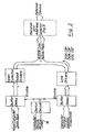
- a suitable digital computer 10 for the CONBUS system 12 is the NOVA * 2-10 (Registered Trade Mark - Data General Corporation) minicomputer.
- This minicomputer can address up to 63 peripheral devices via a device select bus 18 by assigning them a unique 6 bit code.
- Many device codes are pre-assigned to standard devices e.g. printers 14, v.d.u's 16, magnetic tapes, discs etc.
- the CONBUS system can be used with any similar minicomputer.
- the CONBUS system in a preferred embodiment allows up to 32,000 further devices to be rapidly controlled, addressed or given data, as . described hereinafter.
- the CONBUS system is concerned with the method by which additional peripheral devices are addressed.
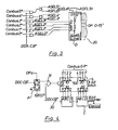
- Data on the bus plus the 1st (A) control line DOA are used to address 0 devices in groups of 16.
- a receiver and address selector is used to decode signals on CONBUS to make their device specific.
- a typical receiver and address selector 20 is shown in Figure 3.
- the sixteen data lines CBO-15 - from the computer interface are buffered and inverted to become CONBUS 0-15 + .
- the 6 least significant bits (LSB'S) are gated with the output control signal DOA.CB + .
- the four least significant bits form ASEL' 0-3 + .
- the two most significant bits (MSB's) are available in both true and compliment form as ASEL 4 t and ASEL 5 ⁇ .
- ASEL 0-3 + form the address inputs to a 75154 4-line-to-16-line decoder D which produces a mutually exclusive output on 1 of the 16 output lines when both enable inputs G l .and G 2 are low. If we assume as stated above that CONBUS is attached to 4 areas of apparatus, the four combinations of ASEL 4 ⁇ and ASEL 5 ⁇ are used to ensure that the decoders similar to D (not shown) in each of the 4 areas are exclusively addressed.
- CONBUS The type of device that may be connected to CONBUS can fall into one of three categories
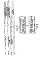
- control can be by one of the decoder D outputs directly - hence only a single software output instruction is required for this form of control.
- a D- flip flop F is preset by one of the outputs of the decoder D (OPx) shown in Figure 3 putting its Q output high which enables the passage of the DOC.CB + given by a second NOVA I/O instruction signal through the NAND gate N. to enable the 8- bit latch L. Data associated with DOC.CB + is therefore loaded into the latch L to program the counter.
- the inverted version of DOC (DOC.CB - ) clocks the D- flip flop F with its rising edge to effectively disable the system holding data within the latch (and hence the counter) stable and to free CONBUS for further transfers to other devices.
- Addressable devices in group (c) require an additional but identical step to be inserted prior to the process described above.
- the address within the selected device is provided by data on CONBUS associated with DOB.CB + and information is loaded by DOC.CB as described. After both steps the address is cleared as in Figure 4.
Landscapes
- Engineering & Computer Science (AREA)
- Theoretical Computer Science (AREA)
- Physics & Mathematics (AREA)
- General Engineering & Computer Science (AREA)
- General Physics & Mathematics (AREA)
- Feedback Control In General (AREA)
- Control By Computers (AREA)
- Magnetic Resonance Imaging Apparatus (AREA)
- Control Or Security For Electrophotography (AREA)
Applications Claiming Priority (2)
| Application Number | Priority Date | Filing Date | Title |
|---|---|---|---|
| GB8101174 | 1981-02-02 | ||
| GB8101174 | 1981-02-02 |
Publications (2)
| Publication Number | Publication Date |
|---|---|
| EP0057515A2 true EP0057515A2 (de) | 1982-08-11 |
| EP0057515A3 EP0057515A3 (de) | 1984-10-24 |
Family
ID=10518990
Family Applications (1)
| Application Number | Title | Priority Date | Filing Date |
|---|---|---|---|
| EP82300166A Withdrawn EP0057515A3 (de) | 1981-02-02 | 1982-01-13 | Signalgeneratoren |
Country Status (4)
| Country | Link |
|---|---|
| US (1) | US4535403A (de) |
| EP (1) | EP0057515A3 (de) |
| JP (1) | JPS57174706A (de) |
| GB (1) | GB2092341B (de) |
Cited By (1)
| Publication number | Priority date | Publication date | Assignee | Title |
|---|---|---|---|---|
| EP0321044A3 (en) * | 1987-12-18 | 1990-08-08 | N.V. Philips' Gloeilampenfabrieken | Data bus control of rom units in information processing system |
Families Citing this family (4)
| Publication number | Priority date | Publication date | Assignee | Title |
|---|---|---|---|---|
| US5274795A (en) * | 1989-08-18 | 1993-12-28 | Schlumberger Technology Corporation | Peripheral I/O bus and programmable bus interface for computer data acquisition |
| US5201055A (en) * | 1989-11-03 | 1993-04-06 | Compaq Computer Corporation | Multiprocessing system includes interprocessor encoding and decoding logic used for communication between two cards through reduced addressing lines |
| US5379404A (en) * | 1990-03-16 | 1995-01-03 | Motorola, Inc. | Plug code for automatically recognizing and configuring both non-microprocessor and microprocessor based radio frequency communication devices |
| US5644790A (en) * | 1994-02-16 | 1997-07-01 | Ati Technologies, Inc. | Universal CD ROM interface using single interface connection |
Family Cites Families (14)
| Publication number | Priority date | Publication date | Assignee | Title |
|---|---|---|---|---|
| GB1142290A (en) * | 1966-05-25 | 1969-02-05 | Gen Electric | Data processing system with improved subsystem communication |
| US3462741A (en) * | 1966-07-25 | 1969-08-19 | Ibm | Automatic control of peripheral processors |
| US3526878A (en) * | 1967-03-27 | 1970-09-01 | Burroughs Corp | Digital computer system |
| US3639909A (en) * | 1970-01-26 | 1972-02-01 | Burroughs Corp | Multichannel input/output control with automatic channel selection |
| US3772656A (en) * | 1971-02-01 | 1973-11-13 | Olivetti & Co Spa | Data communication system between a central computer and data terminals |
| NL7411989A (nl) * | 1974-09-10 | 1976-03-12 | Philips Nv | Computersysteem met busstruktuur. |
| US4079448A (en) * | 1975-04-07 | 1978-03-14 | Compagnie Honeywell Bull | Apparatus for synchronizing tasks on peripheral devices |
| US4124888A (en) * | 1975-12-24 | 1978-11-07 | Computer Automation, Inc. | Peripheral-unit controller apparatus |
| US4115852A (en) * | 1976-12-07 | 1978-09-19 | Harris Data Communications, Inc. | Microprogrammed controller |
| JPS5927929B2 (ja) * | 1977-06-23 | 1984-07-09 | 豊田工機株式会社 | シ−ケンスコントロ−ラ |
| US4158227A (en) * | 1977-10-12 | 1979-06-12 | Bunker Ramo Corporation | Paged memory mapping with elimination of recurrent decoding |
| US4340932A (en) * | 1978-05-17 | 1982-07-20 | Harris Corporation | Dual mapping memory expansion unit |
| US4245300A (en) * | 1978-06-05 | 1981-01-13 | Computer Automation | Integrated and distributed input/output system for a computer |
| US4246637A (en) * | 1978-06-26 | 1981-01-20 | International Business Machines Corporation | Data processor input/output controller |
-
1982
- 1982-01-11 GB GB8200884A patent/GB2092341B/en not_active Expired
- 1982-01-13 EP EP82300166A patent/EP0057515A3/de not_active Withdrawn
- 1982-02-01 JP JP57013414A patent/JPS57174706A/ja active Pending
-
1984
- 1984-06-11 US US06/618,776 patent/US4535403A/en not_active Expired - Fee Related
Cited By (1)
| Publication number | Priority date | Publication date | Assignee | Title |
|---|---|---|---|---|
| EP0321044A3 (en) * | 1987-12-18 | 1990-08-08 | N.V. Philips' Gloeilampenfabrieken | Data bus control of rom units in information processing system |
Also Published As
| Publication number | Publication date |
|---|---|
| JPS57174706A (en) | 1982-10-27 |
| EP0057515A3 (de) | 1984-10-24 |
| GB2092341B (en) | 1984-09-12 |
| US4535403A (en) | 1985-08-13 |
| GB2092341A (en) | 1982-08-11 |
Similar Documents
| Publication | Publication Date | Title |
|---|---|---|
| AU608439B2 (en) | Dynamic feedback arrangement scrambling technique keystream generator | |
| US4470112A (en) | Circuitry for allocating access to a demand-shared bus | |
| EP0112982B1 (de) | Verfahren und Anordnung zur Minimum/Maximum-Bestimmung von Datenwörtern | |
| GB2171543A (en) | Counting circuit which provides for extended counter life | |
| US4602283A (en) | System for spatially and temporally transposing data words arrayed in periodically recurring patterns | |
| EP0057515A2 (de) | Signalgeneratoren | |
| US4319084A (en) | Multichannel digital speech synthesizer | |
| US3340514A (en) | Delay line assembler of data characters | |
| US4202042A (en) | Digital to analog interface for simultaneous analog outputs | |
| US4287768A (en) | Beam deflection method and apparatus for sector scan ultrasound imaging systems | |
| GB2137847A (en) | Picture Image Processing System | |
| US5029171A (en) | Test vector generation system | |
| US2978175A (en) | Program control system for electronic digital computers | |
| US4712072A (en) | Timer apparatus | |
| US4845726A (en) | Maximum length linearly recurring sequence generator control device | |
| US5021990A (en) | Output pulse generating apparatus | |
| US5761100A (en) | Period generator for semiconductor testing apparatus | |
| US5243600A (en) | Time-division multiplexing apparatus | |
| EP0185093A1 (de) | Datenübertragungsvorrichtung | |
| US5355370A (en) | Crosspoint matrix | |
| AU643512B2 (en) | A sequencer for generating binary output signals | |
| US4153944A (en) | Method and arrangement for buffering data | |
| RU1783550C (ru) | Устройство дл моделировани запаздывани сигнала | |
| GB2076571A (en) | A Waveform Generator | |
| Linstadt | Programmable delay unit incorporating a semi-custom integrated circuit |
Legal Events
| Date | Code | Title | Description |
|---|---|---|---|
| PUAI | Public reference made under article 153(3) epc to a published international application that has entered the european phase |
Free format text: ORIGINAL CODE: 0009012 |
|
| AK | Designated contracting states |
Designated state(s): DE FR NL |
|
| PUAL | Search report despatched |
Free format text: ORIGINAL CODE: 0009013 |
|
| AK | Designated contracting states |
Designated state(s): DE FR NL |
|
| STAA | Information on the status of an ep patent application or granted ep patent |
Free format text: STATUS: THE APPLICATION IS DEEMED TO BE WITHDRAWN |
|
| 18D | Application deemed to be withdrawn |
Effective date: 19850625 |
|
| RIN1 | Information on inventor provided before grant (corrected) |
Inventor name: HOLLAND, GEOFFREY NEIL |