EP0057147B1 - Système de test et de visualisation d'états de fonctionnement d'un circuit logique - Google Patents
Système de test et de visualisation d'états de fonctionnement d'un circuit logique Download PDFInfo
- Publication number
- EP0057147B1 EP0057147B1 EP19820400124 EP82400124A EP0057147B1 EP 0057147 B1 EP0057147 B1 EP 0057147B1 EP 19820400124 EP19820400124 EP 19820400124 EP 82400124 A EP82400124 A EP 82400124A EP 0057147 B1 EP0057147 B1 EP 0057147B1
- Authority
- EP
- European Patent Office
- Prior art keywords
- logic circuit
- circuit
- input
- simulation
- logic
- Prior art date
- Legal status (The legal status is an assumption and is not a legal conclusion. Google has not performed a legal analysis and makes no representation as to the accuracy of the status listed.)
- Expired
Links
Images
Classifications
-
- G—PHYSICS
- G06—COMPUTING OR CALCULATING; COUNTING
- G06F—ELECTRIC DIGITAL DATA PROCESSING
- G06F11/00—Error detection; Error correction; Monitoring
- G06F11/22—Detection or location of defective computer hardware by testing during standby operation or during idle time, e.g. start-up testing
- G06F11/26—Functional testing
- G06F11/261—Functional testing by simulating additional hardware, e.g. fault simulation
Definitions
- the present invention relates to a system for testing and displaying operating states of a logic circuit.
- This test and display system can allow the study of electronic circuits comprising a plurality of logic components; it can allow, by analogy, the study of the failure or the proper functioning of a logic circuit, for example a hydraulic circuit of which one or more components can be in a state of failure or of good functioning.
- the hydraulic circuit is replaced by an electronic circuit comprising a plurality of logic components whose operation is equivalent, by analogy, to that of the corresponding components of the hydraulic circuit.
- a circuit made up of logic components presents an output whose logic state depends on the state of failure or good functioning of each of the components.
- This circuit can be, as mentioned above, either a circuit to be tested, or a circuit simulating a circuit to be tested.
- Each of the components of the circuit generally has an input which is connected to an output of another component of the circuit and another input which can receive a signal of simulation of the failure or of the good functioning of this component. Thereafter, it will be understood by studying the operation of a circuit, either studying its proper functioning, or studying its failure.
- the systems which make it possible to test the operating state of a logic circuit, by simulating the failure or of the good functioning of the components of this circuit and which also make it possible to visualize the results of this simulation, are generally complicated, expensive and difficult to implement.
- These systems generally include simulation means which make it possible to apply, by control outputs, logic signals for operating simulation on inputs of the circuit to be tested; these systems also include means which make it possible to take from the outputs of the circuit, the logic state of the logic signals resulting from the application of simulation signals to the inputs of the circuit; these means also make it possible to take the logic state of the signals to be applied to the inputs of this circuit.
- the results of the tests thus carried out can be displayed on display means.
- the object of the invention is to remedy these drawbacks and in particular to provide a system for testing and displaying the operating states of a logic circuit, which makes it possible to view the components in a simple and inexpensive manner.
- the logic circuit that we want to test as well as the connections that occur between the components and, on the other hand, at the location of the components on a display screen, information relating to the simulation performed on each component, results of this simulation and possibly other information concerning each component.
- This test and display system involves, in a very simple manner, as will be seen below in detail, a cover which at least partially covers a display screen while occupying in relation to the latter, a predetermined position; this cache carries lines which represent the connections between the determined components of the circuit studied as well as windows which represent these components; the display of information concerning the type of simulation carried out on each component, the result of this simulation and possibly the display of other information relating to each component, is very simple, in the windows carried out on or in the cache ; as will be seen in detail below, the operator who uses the test and display system of the invention only intervenes by indicating to this system the coordinates of the locations of the windows on the screen, so that the he display of information relating to each component and to the circuit is done therein.
- the subject of the invention is a system for testing and visualizing the operating states of a logic circuit, comprising simulation means presenting control outputs for applying logic signals of operating simulation to inputs of this logic circuit. , means for taking from the outputs of this logic circuit the logic state of the signals resulting from the application of the logic simulation signals to the inputs of the logic circuit, and to take the logic state of the signals applied to the inputs of this logic circuit, characterized in that it further comprises display means with screen , a cover capable of at least partially covering the screen, this cover occupying a predetermined position relative to the screen and carrying lines representing connections between certain determined components of said logic circuit, as well as windows representing said determined components, control means connected to the display means and to the sampling means, the control means being able to control the display means so that these display, for each of said determined components, in the windows corresponding respectively to each of these components, information relating at least to the operating state of the corresponding component, to the identification of this component in s the circuit and the possible transmission at the output of the signal received on an input
- control means connected to the display means consist of a processor controlled by data input means, to fix the display of said information on the screen in the windows.
- control means are also connected to the simulation means to trigger these simulation means after acquisition of the data relating to the locations of the information to be displayed on the screen.
- control means are also connected to the simulation means, to control the display of information relating to the logic circuit, at the locations fixed by the data input means, when the simulation means triggered a simulation.
- sampling means are constituted by a multiplexer having multiplexing inputs which are connected to the outputs and to the inputs of the logic circuit, and a control input connected to a control output of the processor , so that the latter successively selects, on an output of the multiplexer, the successive signals corresponding to the successive signals taken from the outputs of the logic circuit, from successive control signals applied to the control input of the multiplexer.
- the logic circuit consists of logic components which each have at least one operating input and one simulation input, a good functioning or failure signal being able to be applied to the input simulation, each component being capable of transmitting on an output, when it is not faulty, an operating signal dependent on an operating signal received on the operating input, the operating input of the first component of the logic circuit constituting the input of this logic circuit and the output of the last component constituting the output of the logic circuit.
- the system further comprises a counter connected to the processor, this counter being initially loaded with a value N - 1, N corresponding to the number of inputs of the sampling means which are connected to the outputs and at the inputs of the logic circuit, this counter making it possible, when its content is equal to 0, to stop the acquisition of the information supplied at the output of the multiplexer.
- the cover is transparent or opaque.
- test and display system is intended more particularly for the study of operation, that is to say the study of the failure or of the proper functioning of a logic circuit but, as we will see, it can allow, by analogy, the study of the operation of various circuits such as hydraulic circuits for example.
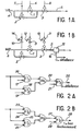
- FIG. 1A schematically represents a hydraulic circuit which makes it possible to establish, for example, the circulation between an upstream conduit 4 and a downstream conduit 5, by means of three pneumatic valves ques 1, 2, 3, the opening or closing of which can be controlled by the presence or absence of compressed air in the control conduits 6, 7,8.
- the valves constitute the only components which can be either in a state of failure, or in a state of good functioning.
- the hydraulic circuit considered is faulty if the fluid is not transmitted in the downstream pipe 5.
- the valves 1 and 2 are faulty, the fluid no longer passes from the upstream pipe 4 to the downstream pipe 5; the same applies when valves 1 and 3 fail. In these two cases, the circuit is put in a state of failure when the aforementioned valves fail.
- Figure 1B schematically represents the circuit of the previous figure in which have been added, for each of the valves 1, 2, 3, on the control conduits 6, 7, 8, of these, means 9, 10, 11 , which simulate the state of failure or proper functioning of these valves.
- a fluid passage detector 12 can be placed on the downstream conduit 5 to indicate, for example, by the presence of a logic state 0 on its output 16, the failure of the hydraulic circuit, when a fluid supplied to the upstream conduit 4, is not found in the downstream conduit 5.
- the means 9, 10, 11, which make it possible to simulate the failure of the valves which correspond to them, have respectively control inputs 13, 14, 15. These means are respectively constituted, for example , by an electrically controlled valve which acts on the pneumatic control of each of the valves 1, 2, 3 of the circuit.
- each of the electrically controlled valves acts so that if a voltage is applied to this input, this valve closes and cuts off the compressed air which arrives in the control duct of the corresponding valve of the hydraulic circuit.
- This shutdown of the compressed air simulates the failure of the corresponding valve in the circuit. This failure being simulated, it then suffices to observe the output signal from the fluid passage detector 12 to know whether or not this failure interrupts the passage of the fluid towards the outlet of the hydraulic circuits.
- FIG. 2A is a logic circuit equivalent to the hydraulic circuit of FIG. 1B; this equivalent circuit makes it possible to study in a simpler and faster way, the state of failure of the hydraulic circuit described above, that is to say its response to simulated failures.
- the valve 1 as well as the electrically controlled valve 9 (which makes it possible to simulate the failure of the valve 1), are replaced by the gate AND i ; a direct input 30 of this door is brought permanently, to a logic level 1, to simulate the arrival of the fluid in the upstream duct of the hydraulic circuit and an inverted input 17 of this door is brought to a logic level 1, to simulate the failure of this circuit.
- the AND gate 2 is equivalent to the valve 2 associated with the simulation valve 10, electrically controlled.
- a level 1 logic state on the input 18 of this door simulates the passage of the fluid, while a level 1 logic state on the reverse input 19 simulates the failure of this door.
- the AND gate 3 is equivalent to the valve 3 and the simulation valve 11, electrically controlled.
- the direct input 20 of this door brought to a logic state 1, simulates the passage of the fluid, while the reverse input 21, brought to a logic state 1, simulates the failure of this door.
- the OR gate 1 is equivalent to the junction between the outputs of the valves 1 and 2.
- This circuit equivalent to the hydraulic circuit of FIG. 1B is considered to be in a fault state when the output 21 of the AND gate 3 is at a logic level 0.
- the circuit of Figure 2B is a logic circuit equivalent to the hydraulic circuit of Figure 1B; it makes it possible to study for example, the state of good functioning of this hydraulic circuit, according to the states of good functioning, simulated on each of its components.
- the valves 1, 2, 3 as well as their simulation control valves 9, 10, 11, with electric control are respectively replaced by the doors ET 4 , ET S , and ET 6 .
- the OR gate 2 represents the junction between the outputs of the valves 1 and 2.
- the AND gates 4 , AND 5 and AND 6 have operating inputs 23, 25, 27 which can be brought to a logic level 1, for simulate the arrival of the fluid at the inlet of the corresponding valve.
- the inputs 24, 26, 28 of these doors make it possible to simulate the proper functioning of each of the valves, when they are brought to a logic level 1. If the circuit is in a functioning state, the output 29 of the gate AND 6 is at a logic level 1, when a level 1 simulating the arrival of the fluid at the inlet of the hydraulic circuit is permanently applied to the inlet 23 of the first gate AND 4 .
- this logic circuit equivalent to the hydraulic circuit of FIG. 1B makes it possible to study the state of proper functioning of the hydraulic circuit, as a function of the state of proper functioning of each of its components.
- the test and display system acts so as to apply, for example to each of the fault simulation or correct operation inputs of the AND gates of FIGS. 2A and 2B, level 1 logic signals making it possible to simulate the proper functioning or failure of each of these doors; this system then makes it possible to view in a simple manner, relative information in particular in the state of failure or of correct functioning of the circuit and of its components, as a function of the simulation signals applied to each component. It also makes it possible to view information relating to the simulation signals and to the ranks or marks of the components to which these simulation signals are applied.
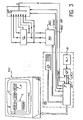
- FIG. 3 schematically represents a test and display system, in accordance with the invention.
- This system makes it possible to test the logical operating states of a logic circuit (CL) which is constituted, as will be seen later in detail, by a set of logic components.
- This system includes simulation means (MS) which have control outputs making it possible to apply logic simulation, operating signals, to inputs of the circuit (CL).
- Means (MP) make it possible to take from the outputs of the circuit (CL) the logic state of the signals on these outputs and to take the logic state from the simulation signals applied to the inputs of the circuit (CL).
- the system also comprises display means (MV) with screen (E) as well as a cover (C) which at least partially covers the screen (E) and which occupies a predetermined position relative to the latter.
- This cover has lines (L) and windows (F). These lines represent the connections between some of the determined components of the circuit, while the windows (F) represent these components.
- the system also includes control means (MC) which are connected to the display means (MV) as well as to the sampling means (MP).
- control means make it possible, as will be seen in detail below, to control the display means (MV) so that these display, for each of the determined components of the circuit (CL), in the windows (F) corresponding to each of these components, information relating to the operating state of the corresponding component, the location of this component in the circuit and the possible transmission at output, of the signal received on an input of the component.
- the control means (MC) consist of a process (P), controlled by data input means (ED), which make it possible to fix the display of information relating to the test of the logic circuit (CL), in the windows (F).
- These data entry means in fact allow the operator to indicate to the display means (MV), the coordinates of these windows, so that the information relating to the tests of the circuit (CL), are displayed in these Windows.
- the means (ED) of data entry can be constituted by a read-only memory containing all the data concerning the coordinates of the windows (F), to control displaying information in these windows.
- control means (MC) which are connected to the display means (MV) and to the sampling means (MP), are also connected to the simulation means (MS), to trigger these simulation means as will be seen below. in detail, after acquisition of the data relating to the locations of the information to be displayed on the screen (E).
- control means (MC) are connected to the simulation means (MS) so as to control the display of information relating to the circuit to be tested, at the locations fixed by the data input means, when the simulation means (MS) triggered a simulation, autonomously, that is to say without specific order received from the control means (MC).
- the sampling means (MP) consist of a multiplexer which has multiplexing inputs respectively connected to the outputs and the inputs of the logic circuits (CL) to be tested.
- This multiplexer also has a control input connected to a control output of the processor (P) so as to receive a control signal SYNC. It is this control signal which makes it possible to select successively on an output (0) of the multiplexer, the signals sampled successively on the outputs and the inputs of the circuit (CL).
- This multiplexer also has another control input connected to a processor control output (P) so that the latter applies to the multiplexer a RAZMP signal which makes it possible to reset this multiplexer when the latter has successively selected all the signals present on its inputs or initialize this multiplexer before a series of sampling.
- P processor control output
- the circuit (CL) can for example be one of the circuits of FIGS. 2A or 2B; it consists, as described above, of logic components which each have at least one operating input and one simulation input; the simulation inputs of the various components receive simulation means (MS) of logic signals of level 1 or 0, which simulate either the correct operation or the failure of the corresponding component.
- the simulation means (MS) may for example be those described in French patent application No. 81 01 392 filed on January 26, 1981 in the name of the same applicant and which is entitled “Generator of combined logic signals •.
- the operating input of the first component constitutes the input of the circuit
- the output of the last component constitutes the output of the circuit.
- control means (MC) further comprise a counter (CP) connected to the processor (P); this counter which intervenes as will be described later in detail, is initially loaded with a value N - 1, in which N corresponds to the number of inputs of the sampling means (MP) which are connected to the outputs and the inputs of the logic circuit ( CL).
- This counter can be loaded initially with the value N - 1, for example via a register (R). This loading can be carried out on the reception of an INIT command from the processor (P).
- the counter (CP) also makes it possible to stop, by a signal (ST) supplied to the processor (P), the acquisition of the test information supplied on the outputs of the multiplexer (MP).
- the cover (C) which occupies a predetermined position relative to two axes of fictitious XY coordinates linked to the screen (E), can be a transparent cover on which the windows and the connections between these windows have been drawn or, a cover opaque on which the connections were drawn and in which the windows were cut.
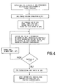
- FIG. 4 is a flowchart which makes it possible to better understand the operation of the system of the invention.
- the first operation consists in recording in a random access memory for example (not shown) of the processor (P), from the data input means (ED), the coordinates of the windows carried by the cache (C), so that the results of the circuit tests (CL) are displayed on the screen, next to the windows corresponding to each component respectively.
- the data which is stored in the RAM of the processor (P) also includes the numbers of the components corresponding to each window, these numbers being chosen in a predetermined manner.
- the data entry means (ED) can be constituted, for example, by a data entry keyboard, well known in the state of the art.
- the second operation consists in commanding the sending of simulation signals to the inputs of the logic circuit to be tested (CL), from the simulation means (MS).
- This command can be an autonomous trigger command applied to a command input DEC of the simulation means (MS), which then warn by a suitable signal the processor (P), that the simulation is triggered; this triggering can also be caused by an appropriate signal from the processor (P).
- the simulation signals applied to the inputs of the logic circuit (CL) can be constituted for example by combined logic signals, of level 0 or 1, formed by the generator described in the aforementioned patent application. As indicated above, the inputs of the multiplexer (MP) are connected on the one hand, to the outputs of the simulation means (MS) and on the other hand, to the outputs of the logic circuit (CL).
- the following operation consists in resetting the multiplexer (MP) to zero by a RAZMP signal and in loading the counter (CP) to the value N - 1 in which N corresponds to the number of inputs of the multiplexer (MP).
- This loading can be carried out for example from a register (R).
- This counter is loaded at the value N - 1 when it receives from the processor (P) an initialization signal INIT.
- This counter also makes it possible, as will be seen below in detail, to stop the progress of the display operations controlled by the processor (P) when it sends to the latter a stop signal (ST), when its content is zero.
- the multiplexer (MP) When the multiplexer (MP) has been reset, the information available on the output of this multiplexer corresponds to the logic signal which is applied to the first input thereof. This information is then loaded into the RAM of the processor (P) (not shown). The processor (P) obviously processes this information in relation to the data corresponding to the coordinates of the information to be displayed in the windows on the screen.
- this information is read at the output of the multiplexer (MP) and possibly stored, either in an internal memory of the multiplexer, or in a display memory (MV), or in the memory of the processor (P) in conjunction, in an orderly fashion with the number of the corresponding component; in fact, as indicated above, the RAM of the processor (P) contains the coordinates for displaying the information of each component in the corresponding windows.
- the decrementing of the content of the counter (CP) is accompanied by the sending to the multiplexer (MP) of a SYNC control signal from this multiplexer which makes it possible to take into account on the output of this multiplexer, the information corresponding to the signal. present on the next input of the multiplexer.
- the processor can then command the display, in the windows corresponding to each component, of information successively taken from the output of the multiplexer (MP) and provisionally stored, either in a memory of the multiplexer (MP), either in a memory of the processor (P), or possibly in a memory of the display means (MV).
- the information which appears in the windows F 1 of the cover (C) on which the connections between the various determined components of the circuit appear is of several types. If we consider the first box of each window, the information displayed, thanks to the system described above, can be the letter P or the sign (-) for example, which respectively denote either the failure of the corresponding component, or on the contrary the non-failure state of this component.
- the following two boxes in each window relate to the information which is, for example, in the figure, 01, 02, 03, 04, ...; this information corresponds to the numbers that we have chosen to assign to each component, prior to the tests.
- the last box contains for example an asterisk or a sign (-); these signs respectively indicate that the signal present at the input of the component is not transmitted at output or that on the contrary, the signal present at input is transmitted at the output of this one.
- FIG. 3 which corresponds to the test of the circuit in FIG. 2A
- Components 3 and 4 are not faulty, but they do not transmit any output signal since they do not in fact receive any output signal from components 1 and 2.
Landscapes
- Engineering & Computer Science (AREA)
- Computer Hardware Design (AREA)
- General Engineering & Computer Science (AREA)
- Theoretical Computer Science (AREA)
- Quality & Reliability (AREA)
- Physics & Mathematics (AREA)
- General Physics & Mathematics (AREA)
- Tests Of Electronic Circuits (AREA)
- Test And Diagnosis Of Digital Computers (AREA)
- Logic Circuits (AREA)
Applications Claiming Priority (2)
| Application Number | Priority Date | Filing Date | Title |
|---|---|---|---|
| FR8101463A FR2498763A1 (fr) | 1981-01-27 | 1981-01-27 | Systeme de test et de visualisation d'etats de fonctionnement d'un circuit logique |
| FR8101463 | 1981-01-27 |
Publications (2)
| Publication Number | Publication Date |
|---|---|
| EP0057147A1 EP0057147A1 (fr) | 1982-08-04 |
| EP0057147B1 true EP0057147B1 (fr) | 1985-01-09 |
Family
ID=9254545
Family Applications (1)
| Application Number | Title | Priority Date | Filing Date |
|---|---|---|---|
| EP19820400124 Expired EP0057147B1 (fr) | 1981-01-27 | 1982-01-22 | Système de test et de visualisation d'états de fonctionnement d'un circuit logique |
Country Status (4)
| Country | Link |
|---|---|
| EP (1) | EP0057147B1 (show.php) |
| JP (1) | JPS57147072A (show.php) |
| DE (1) | DE3261786D1 (show.php) |
| FR (1) | FR2498763A1 (show.php) |
Family Cites Families (3)
| Publication number | Priority date | Publication date | Assignee | Title |
|---|---|---|---|---|
| US3562644A (en) * | 1968-06-14 | 1971-02-09 | Nicholas De Wolf | Circuit tester providing circuit-selected test parameters |
| US3881260A (en) * | 1973-07-05 | 1975-05-06 | James M Hombs | Self-teaching machine for binary logic |
| US3924181A (en) * | 1973-10-16 | 1975-12-02 | Hughes Aircraft Co | Test circuitry employing a cyclic code generator |
-
1981
- 1981-01-27 FR FR8101463A patent/FR2498763A1/fr active Granted
-
1982
- 1982-01-22 DE DE8282400124T patent/DE3261786D1/de not_active Expired
- 1982-01-22 EP EP19820400124 patent/EP0057147B1/fr not_active Expired
- 1982-01-25 JP JP57009950A patent/JPS57147072A/ja active Pending
Also Published As
| Publication number | Publication date |
|---|---|
| EP0057147A1 (fr) | 1982-08-04 |
| FR2498763B1 (show.php) | 1983-02-18 |
| JPS57147072A (en) | 1982-09-10 |
| DE3261786D1 (en) | 1985-02-21 |
| FR2498763A1 (fr) | 1982-07-30 |
Similar Documents
| Publication | Publication Date | Title |
|---|---|---|
| EP0642683B1 (fr) | Procede et plate-formes de test pour le developpement d'un circuit integre | |
| FR2531230A1 (fr) | Ensemble destine au test automatique centralise de circuits imprimes et procede de test de circuits a microprocesseur faisant application de cet ensemble | |
| FR2585476A1 (fr) | Dispositif et procede de localisation de defauts pour l'essai de plaquettes de circuit | |
| EP0481881A1 (fr) | Circuit intégré à sécurité d'accès amélioré | |
| EP1980941A1 (fr) | Système de création automatisée d'une interface logicielle | |
| CA2696020A1 (fr) | Procede de generation automatique de script pour tester la validite d'un logiciel de fonctionnement d'un systeme embarque a bord d'un aeronef, et dispositif de mise en oeuvre | |
| EP2150897B1 (fr) | Procede de simulation d'un systeme embarque a bord d'un aeronef pour tester un logiciel de fonctionnement et dispositif pour la mise en oeuvre de ce procede | |
| FR2903384A1 (fr) | Systeme de commande de vol pour aeronef,et systeme de test pour tester un tel systeme de commande de vol. | |
| FR2724744A1 (fr) | Procede de modelisation d'un processus physique | |
| FR2473766A1 (fr) | Dispositif d'affichage de blocs de sequences | |
| EP0057147B1 (fr) | Système de test et de visualisation d'états de fonctionnement d'un circuit logique | |
| FR2532771A1 (fr) | Procede et dispositif pour tester statiquement l'ensemble des connexions et des circuits integres peripheriques d'un microprocesseur | |
| FR2684211A1 (fr) | Dispositif d'exploitation des informations relatives aux pannes detectees par une ou plusieurs unites centrales d'un aeronef. | |
| EP1593982A1 (fr) | Contrôle de la robustesse d'une modélisation d'un système physique | |
| CA1256498A (fr) | Appareil universel de detection de defectuosites dans des systemes a microprocesseur | |
| FR2658933A1 (fr) | Systeme de commande du deroulement de sequences de tests dans un appareil de traitement de l'information. | |
| CA2020505C (fr) | Procede d'assistance pour l'utilisateur d'un systeme informatique et dispositif pour la mise en oeuvre dudit procede | |
| EP0985155B1 (fr) | Procede et dispositif de test pour equipements electroniques | |
| EP0174220A1 (fr) | Système de test de la défaillance ou du bon fonctionnement d'un circuit à composants logiques | |
| EP0683455B1 (fr) | Circuit intégré comprenant des moyens pour arrêter l'exécution d'un programme d'instructions quand une combinaison de points d'arrêt est vérifiée | |
| FR2751082A1 (fr) | Dispositif de commutation notamment de systeme sous test | |
| FR2458850A1 (fr) | Moniteur de station de maintenance et station de maintenance le comprenant | |
| EP0674265B1 (fr) | Procédé et dispositif d'élaboration de tests de cartes électroniques | |
| EP0823088B1 (fr) | Procede et equipement de test automatique en parallele de composants electroniques | |
| EP0060194B1 (fr) | Système de test de la défaillance ou du bon fonctionnement d'un circuit à composants logiques |
Legal Events
| Date | Code | Title | Description |
|---|---|---|---|
| PUAI | Public reference made under article 153(3) epc to a published international application that has entered the european phase |
Free format text: ORIGINAL CODE: 0009012 |
|
| AK | Designated contracting states |
Designated state(s): BE DE GB IT LU NL SE |
|
| 17P | Request for examination filed |
Effective date: 19830112 |
|
| ITF | It: translation for a ep patent filed | ||
| GRAA | (expected) grant |
Free format text: ORIGINAL CODE: 0009210 |
|
| PGFP | Annual fee paid to national office [announced via postgrant information from national office to epo] |
Ref country code: DE Payment date: 19841219 Year of fee payment: 4 |
|
| AK | Designated contracting states |
Designated state(s): BE DE GB IT LU NL SE |
|
| PG25 | Lapsed in a contracting state [announced via postgrant information from national office to epo] |
Ref country code: LU Free format text: LAPSE BECAUSE OF NON-PAYMENT OF DUE FEES Effective date: 19850131 |
|
| REF | Corresponds to: |
Ref document number: 3261786 Country of ref document: DE Date of ref document: 19850221 |
|
| PLBE | No opposition filed within time limit |
Free format text: ORIGINAL CODE: 0009261 |
|
| STAA | Information on the status of an ep patent application or granted ep patent |
Free format text: STATUS: NO OPPOSITION FILED WITHIN TIME LIMIT |
|
| 26N | No opposition filed | ||
| PGFP | Annual fee paid to national office [announced via postgrant information from national office to epo] |
Ref country code: NL Payment date: 19870131 Year of fee payment: 6 |
|
| PG25 | Lapsed in a contracting state [announced via postgrant information from national office to epo] |
Ref country code: GB Effective date: 19890122 |
|
| PG25 | Lapsed in a contracting state [announced via postgrant information from national office to epo] |
Ref country code: SE Effective date: 19890123 |
|
| PG25 | Lapsed in a contracting state [announced via postgrant information from national office to epo] |
Ref country code: BE Effective date: 19890131 |
|
| BERE | Be: lapsed |
Owner name: COMMISSARIAT A L'ENERGIE ATOMIQUE ETABLISSEMENT D Effective date: 19890131 |
|
| PG25 | Lapsed in a contracting state [announced via postgrant information from national office to epo] |
Ref country code: NL Effective date: 19890801 |
|
| NLV4 | Nl: lapsed or anulled due to non-payment of the annual fee | ||
| GBPC | Gb: european patent ceased through non-payment of renewal fee | ||
| PG25 | Lapsed in a contracting state [announced via postgrant information from national office to epo] |
Ref country code: DE Effective date: 19891003 |
|
| EUG | Se: european patent has lapsed |
Ref document number: 82400124.2 Effective date: 19891204 |