EP0056482B1 - Glass passivation semiconductor device and method of manufacturing the same - Google Patents
Glass passivation semiconductor device and method of manufacturing the same Download PDFInfo
- Publication number
- EP0056482B1 EP0056482B1 EP81110699A EP81110699A EP0056482B1 EP 0056482 B1 EP0056482 B1 EP 0056482B1 EP 81110699 A EP81110699 A EP 81110699A EP 81110699 A EP81110699 A EP 81110699A EP 0056482 B1 EP0056482 B1 EP 0056482B1
- Authority
- EP
- European Patent Office
- Prior art keywords
- glass
- passivation
- semiconductor device
- stress relaxing
- relaxing layer
- Prior art date
- Legal status (The legal status is an assumption and is not a legal conclusion. Google has not performed a legal analysis and makes no representation as to the accuracy of the status listed.)
- Expired
Links
Images


Classifications
-
- H—ELECTRICITY
- H10—SEMICONDUCTOR DEVICES; ELECTRIC SOLID-STATE DEVICES NOT OTHERWISE PROVIDED FOR
- H10P—GENERIC PROCESSES OR APPARATUS FOR THE MANUFACTURE OR TREATMENT OF DEVICES COVERED BY CLASS H10
- H10P14/00—Formation of materials, e.g. in the shape of layers or pillars
- H10P14/60—Formation of materials, e.g. in the shape of layers or pillars of insulating materials
- H10P14/69—Inorganic materials
- H10P14/692—Inorganic materials composed of oxides, glassy oxides or oxide-based glasses
- H10P14/6921—Inorganic materials composed of oxides, glassy oxides or oxide-based glasses containing silicon
- H10P14/6922—Inorganic materials composed of oxides, glassy oxides or oxide-based glasses containing silicon the material containing Si, O and at least one of H, N, C, F or other non-metal elements, e.g. SiOC, SiOC:H or SiONC
- H10P14/6923—Inorganic materials composed of oxides, glassy oxides or oxide-based glasses containing silicon the material containing Si, O and at least one of H, N, C, F or other non-metal elements, e.g. SiOC, SiOC:H or SiONC the material being boron or phosphorus doped silicon oxides, e.g. BPSG, BSG or PSG
-
- H—ELECTRICITY
- H10—SEMICONDUCTOR DEVICES; ELECTRIC SOLID-STATE DEVICES NOT OTHERWISE PROVIDED FOR
- H10P—GENERIC PROCESSES OR APPARATUS FOR THE MANUFACTURE OR TREATMENT OF DEVICES COVERED BY CLASS H10
- H10P14/00—Formation of materials, e.g. in the shape of layers or pillars
- H10P14/60—Formation of materials, e.g. in the shape of layers or pillars of insulating materials
- H10P14/63—Formation of materials, e.g. in the shape of layers or pillars of insulating materials characterised by the formation processes
- H10P14/6326—Deposition processes
- H10P14/6328—Deposition from the gas or vapour phase
- H10P14/6334—Deposition from the gas or vapour phase using decomposition or reaction of gaseous or vapour phase compounds, i.e. chemical vapour deposition
-
- H—ELECTRICITY
- H10—SEMICONDUCTOR DEVICES; ELECTRIC SOLID-STATE DEVICES NOT OTHERWISE PROVIDED FOR
- H10W—GENERIC PACKAGES, INTERCONNECTIONS, CONNECTORS OR OTHER CONSTRUCTIONAL DETAILS OF DEVICES COVERED BY CLASS H10
- H10W74/00—Encapsulations, e.g. protective coatings
- H10W74/10—Encapsulations, e.g. protective coatings characterised by their shape or disposition
- H10W74/131—Encapsulations, e.g. protective coatings characterised by their shape or disposition the semiconductor body being only partially enclosed
- H10W74/134—Encapsulations, e.g. protective coatings characterised by their shape or disposition the semiconductor body being only partially enclosed the encapsulations being in grooves in the semiconductor body
-
- H—ELECTRICITY
- H10—SEMICONDUCTOR DEVICES; ELECTRIC SOLID-STATE DEVICES NOT OTHERWISE PROVIDED FOR
- H10P—GENERIC PROCESSES OR APPARATUS FOR THE MANUFACTURE OR TREATMENT OF DEVICES COVERED BY CLASS H10
- H10P14/00—Formation of materials, e.g. in the shape of layers or pillars
- H10P14/60—Formation of materials, e.g. in the shape of layers or pillars of insulating materials
- H10P14/69—Inorganic materials
- H10P14/692—Inorganic materials composed of oxides, glassy oxides or oxide-based glasses
- H10P14/6921—Inorganic materials composed of oxides, glassy oxides or oxide-based glasses containing silicon
- H10P14/69215—Inorganic materials composed of oxides, glassy oxides or oxide-based glasses containing silicon the material being a silicon oxide, e.g. SiO2
Definitions
- the present invention relates to a high voltage withstanding glass passivation semiconductor device and a method of manufacturing the same.
- the semiconductor device of beveled structure is poor in damp-proofness because the film for protecting its junction surface is made of organic material such as silicone. In addition, it is liable to cause leakage current according to the high temperature bias test. It is therefore lack of reliability.
- the semiconductor device of guard ring structure is liable to deteriorate its characteristic because SiO z film which is used as the protection film for stabilizing the surface of semiconductor elements is so thin as to cause electric field to have its effect even outside SiO 2 film.
- a high voltage withstanding semiconductor device which uses glass material as the passivation film so as to eliminate above-mentioned drawbacks (hereinafter referred to as "glass passivation semiconductor device") has been put to practical use these days.
- An example of this device is disclosed in the Japanese Patent Publication (Kokoku) No. 42668/78.
- This glass passivation semiconductor device is usually manufactured by 1) chemically mesa- etching the junction formed in a semiconductor substrate or cutting the junction in parallel crosses by a diamond blade to form a recess, 2) filling glass material in the etched region or recess according to electrophoresis method, for example, and 3) sintering glass material filled.
- the glass passivation semiconductor device thus manufactured has higher reliability than conventional high voltage withstanding semiconductor devices as already mentioned above.
- this glass passivation semiconductor device In the case of this glass passivation semiconductor device, however, internal stress is generated in the semiconductor substrate causing the semiconductor substrate to be bent in concave because coefficient of thermal expansion of glass material filled in the recess or etched region is different from that of semiconductor substrate.
- the semiconductor substrate or wafer therefore breaks and cracks are caused in glass material in the subsequent photoetching process.
- glass or pellet cracks are easily caused even in the semiconductor device or pellet having no glass crack in the assembly after the dicing or scribing process.
- the semiconductor device having glass or pellet cracks is poor in dielectric strength. The yield of glass passivation semiconductor devices conventionally manufactured is low accordingly.
- Document GB-A-2 003 662 discloses a method for stabilizing the surface treatment of a semiconductor body.
- recesses are intersected in PN junction surfaces, and after cleaning the semiconductor surface by etching a thin layer of the oxide of the semiconductor material and three further sublayers of a glass having decreasing thermal expansion coefficients are formed one after another in the recesses so as to avoid cracks in the entire glass coat.
- This method does not use a surface stabilizing protection film, and the three glass sublayers having two different thermal expansion coefficient result in a complicated structure.
- the object of the present invention is to provide a glass passivation semiconductor device capable of preventing cracks from being caused in the passivation glass.
- a glass passivation semiconductor device comprising a PN junction region formed by first and second semiconductor regions, a passivation glass directly formed on said PN junction and a stress relaxing layer formed on said passivation glass, said semiconductor device being characterized in that a surface stabilizing protection film covers at least one of said first and second semiconductor regions, and said stress relaxing layer is tightly contacted with said protection film so as to relax stress in said passivation glass.
- the stress relaxation layer covers the surface stabilizing and protecting film formed on the surface of semiconductor substrate.
- the glass passivation semiconductor device thus manufactured causes almost no glass crack to thereby enhance the yield thereof.
- the glass passivation semiconductor device is therefore suitable for mass production.
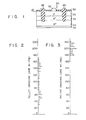
- Fig. 1 shows a high voltage withstanding diode device 20 having glass passivation regions 22 and the diode device 20 will be hereinafter referred to as "a diode pellet".
- This diode pellet 20 comprises an N + layer 24, and N- layer 26 formed on the N + layer 24, a P-type region 28 formed on the N-layer 26, glass passivation regions 22 formed in recesses each having a depth which reaches the N + layer 24, a protection film 30 made of Si0 2 and formed on the P-type region 28 to stabilize the surface of semiconductor, an electrode 32 connected to the P-type region 28 and an electrode 34 connected to the N + layer 24.
- Recesses are formed by the chemical etching process or a diamond blade.
- Glass passivation regions 22 are formed by filling glass material in recesses according to the electrophoresis method, for example, and sintering the field glass material at the temperature of about 700°C.
- the bending test was carried out using a plurality of diode pellets thus formed. Namely, leakage current in each of diode pellets was measured applying reverse bias to the PN junction of each of diode pellets and adding load to each of diode pellets. Load which causes short-circuited current or leakage current to flow was regarded as pellet cracking load W1, the short-circuited current being a current caused when the pellet itself cracks and the leakage current being larger current than initial leakage current generated when glass cracks are caused.
- Fig. 2 shows the result thus obtained.
- Fig. 3 also shows the result obtained by same measurements using pellets of beveled structure. As apparent from the comparison of Figs. 2 and 3, pellet cracking load W1 in the glass passivation semiconductor device is lower than that in the semiconductor device of beveled structure and dispersed in a wider range.
- Fig. 4 shows the result of bending test carried out using diode pellets in which glass cracks are already caused before the bending test
- Fig. 5 also shows the result of bending test carried out using diode pellets in which no glass crack is caused before the bending test. It was found from these results that diode pellets in which pellet cracking load W1 is low had glass cracks caused before the bending test.
- pellet cracking load W1 was dispersed in Fig. 5
- diode pellets were made using glass material of various glass strengths. The bending test was carried out using these diode pellets. Some little difference was found in the occurrence of glass cracks, but no large difference was found in pellet cracking load W1 after glass cracks were caused. It was guessed from this result that pellet cracks were generated by some other cause, namely, the shape of pellet. As the result of bending test of pellets having various passivation glass swells from the surface of semi-conductor substrate, it was recognized that the dispersion of pellet cracking load W1 depended upon the uneven shape of passivation glass.
- Fig. 7 is a graph showing the relation between the swell (d) of passivation glass and load W2 by which cracks are caused in passivation glass and which will be hereinafter referred to as "glass cracking load".
- the swell (d) is + (plus) when the surface of glass material is higher than the surface of semiconductor substrate and - (minus) when the former is lower than the latter.
- the strength of passivation glass is the largest when the surface of passivation glass is substantially same in level as the surface of semi-conductor substrate.
- the dispersion range (about 60 kg) of glass cracking load W2 in Fig. 7 is substantially equal to that (about 60 kg) of pellet cracking load W1 in Fig. 5.
- pellet cracking load W1 becomes large as glass cracking load W2 becomes large. Because the pellet cracking load W1 is nearly equal to the sum of the glass cracking load W2 and a load for cracking the pellet in which the glass crack is caused.
- the swell (d) of passivation glass is in the range of about ⁇ 7 11m for the purpose of making glass cracking load W2 larger than 80 kg.
- the distribution range of glass swell (d) formed by the glass filling and sintering process is usually ⁇ 5-6 11m under same manufacturing condition but practically becomes larger since the center in the distribution range of glass swell (d) is shifted. It is therefore extremely difficult to keep the swell (d) of passivation glass in the range of ⁇ 7 pm, thus reducing the yield of diode pellets.
- the strength of passivation glass is increased so as to enhance the strength of glass passivation semiconductor device.
- the strength of passivation glass depends upon the swell (d) of passivation glass. This means that internal stress present in passivation glass changes corresponding to the change of swell (d). This was the reason why the inventor of the present invention formed a stress relaxing layer on passivation glass to relax internal stress in passivation glass and to prevent cracks from being caused in passivation glass. It is needed that this layer functioning as a stress relaxing layer has an elastic modulus larger than that of passivation glass and can tightly contact relative to both passivation glass and protection film for stabilizing the surface of semiconductor substrate.
- silicon oxide (Si0 2 ), boron-silicate glass (BSG) and phospho-silicate glass (PSG) were vapor-deposited respectively at low temperature on Si0 2 protection film and passivation glass according to CVD method.
- Phospho-silicate glass showed a remarkable stress relaxing effect. It was also found that the stress relaxing effect became higher as phospho-silicate glass had higher phosphorus concentration and that phospho-silicate glass was needed to have a layer thickness larger than 1 ⁇ m. It is needed that phospho-silicate glass tightly contacts with Si0 2 protection film at the end portion thereof.
- Fig. 8 is a sectional view showing a diode pellet 120.
- An N-layer 126 is formed on an N +- type semiconductor substrate 124.
- a P-type region 128 is formed thermally diffusing P-type impurity in the N- layer 126.
- a surface stabilizing protection film 130 consisting of SiO z , for example, is then formed on the P-type region 128.
- Recesses each passing through the protection film 130, P-type region 128 and N- layer 126 and reaching the N +- type semi- conductor substrate 124 are formed by chemical etching or diamond blade. Passivation glass material is filled in recesses according to electrophoresis method.
- Glass material filled is sintered at temperature of 600°C-700°C to form glass passivation regions 122.
- Phospho-silicate glass is deposited on glass passivation regions 122 according to CVD method to form a stress relaxing layer 136. It is necessary that this chemical vapor deposition is carried out in an atmosphere lower than the sintering temperature of passivation glass, because passivation glass is so softened as to flow out of recesses or to have chemical change in an atmosphere higher than about 700°C.
- the stress relaxing layer 136 must have a thickness at least larger than 1 pm. When the thickness of layer 136 is smaller than 1 pm, the stress relaxing effect of passivation glass is negligible.
- the stress relaxing layer 136 is tightly contacted with Si0 2 protection film 130 with a width r at least larger than 30 ⁇ m so as to enhance the contact strength between the stress relaxing layer 136 and Si0 2 protection film 130.
- Si0 2 film 130 is then selectively etched to form an opening in which an electrode 132 connected to P-type region 128 is formed.
- Another electrode 134 is also formed on the back face of N +- type semiconductor substrate 124.
- the stress relaxing layer 136 thus formed at a relatively low temperature is porous and it is guessed that the stress relaxing layer 136 is effective because it is porous.
- Passivation glass regions 122 each having a swell (d) different from those of other passivation glass regions are formed and the stress relaxing layer 136 is formed on passivation glass regions to have a thickness (d) of 1 ⁇ m and a width (r) of 30 ⁇ m.
- the bending test was carried out using diode pellets thus formed.
- Fig. 9 shows the relation between the swell (d) at the passivation glass 122 and glass cracking load W2.
- the swell (d) of passivation glass may be made -10 pm - +15 ⁇ m in order to manufacture a diode pellet whose glass cracking load W2 is larger than 80 kg.
- the glass passivation semiconductor device can be manufactured according to the conventional glass filling technique.
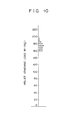
- Fig. 10 shows the distribution of pellet cracking load W1 in the case of diode pellets formed according to the present invention.
- pellet cracking load is in the range of 160-195 kg.
- Diode pellets formed according to the present invention have a higher pellet strength as compared with that of conventional ones, and the dispersion of strength is small in diode pellets of the present invention.
- the ratio of occurrence of pellet or glass crack in pellet manufacturing and assembling processes was reduced to lower than 1-2%.
- the conventional ratio thereof was in the range of 50-60%.
- the embodiment as described above is similar to the conventional mesa-type semiconductor device in which recesses to fill passivation glass therein are deepened.
- the present invention is not limited to the embodiment but applicable to the planar-type glass passivation semiconductor device, whose recesses are shallow, so as to achieve same effect. Therefore, the present invention is suitable for all of glass passivation semiconductor devices.
- the present invention enables pellet strength to be made higher as compared with that of conventional glass passivation semiconductor devices and pellet strength obtained by the present invention becomes substantially equal to that of a high voltage withstanding semiconductor device of beveled structure in which no glass material is employed. Therefore, the present invention can prevent the yield from being reduced due to the occurrence of glass crack and provide a glass passivation semi- conductor device suitable for mass production.
Landscapes
- Formation Of Insulating Films (AREA)
Description
- The present invention relates to a high voltage withstanding glass passivation semiconductor device and a method of manufacturing the same.
- There are conventionally well known high voltage withstanding semiconductor devices of beveled structure and of guard ring structure. However, the semiconductor device of beveled structure is poor in damp-proofness because the film for protecting its junction surface is made of organic material such as silicone. In addition, it is liable to cause leakage current according to the high temperature bias test. It is therefore lack of reliability. On the other hand, the semiconductor device of guard ring structure is liable to deteriorate its characteristic because SiOz film which is used as the protection film for stabilizing the surface of semiconductor elements is so thin as to cause electric field to have its effect even outside SiO2 film.
- A high voltage withstanding semiconductor device which uses glass material as the passivation film so as to eliminate above-mentioned drawbacks (hereinafter referred to as "glass passivation semiconductor device") has been put to practical use these days. An example of this device is disclosed in the Japanese Patent Publication (Kokoku) No. 42668/78.
- This glass passivation semiconductor device is usually manufactured by 1) chemically mesa- etching the junction formed in a semiconductor substrate or cutting the junction in parallel crosses by a diamond blade to form a recess, 2) filling glass material in the etched region or recess according to electrophoresis method, for example, and 3) sintering glass material filled. The glass passivation semiconductor device thus manufactured has higher reliability than conventional high voltage withstanding semiconductor devices as already mentioned above.
- In the case of this glass passivation semiconductor device, however, internal stress is generated in the semiconductor substrate causing the semiconductor substrate to be bent in concave because coefficient of thermal expansion of glass material filled in the recess or etched region is different from that of semiconductor substrate. The semiconductor substrate or wafer therefore breaks and cracks are caused in glass material in the subsequent photoetching process. In addition, glass or pellet cracks are easily caused even in the semiconductor device or pellet having no glass crack in the assembly after the dicing or scribing process. The semiconductor device having glass or pellet cracks is poor in dielectric strength. The yield of glass passivation semiconductor devices conventionally manufactured is low accordingly.
- Document GB-A-2 003 662 discloses a method for stabilizing the surface treatment of a semiconductor body. In this method, recesses are intersected in PN junction surfaces, and after cleaning the semiconductor surface by etching a thin layer of the oxide of the semiconductor material and three further sublayers of a glass having decreasing thermal expansion coefficients are formed one after another in the recesses so as to avoid cracks in the entire glass coat. This method does not use a surface stabilizing protection film, and the three glass sublayers having two different thermal expansion coefficient result in a complicated structure.
- The object of the present invention is to provide a glass passivation semiconductor device capable of preventing cracks from being caused in the passivation glass.
- This object of the present invention is achieved by a glass passivation semiconductor device comprising a PN junction region formed by first and second semiconductor regions, a passivation glass directly formed on said PN junction and a stress relaxing layer formed on said passivation glass, said semiconductor device being characterized in that a surface stabilizing protection film covers at least one of said first and second semiconductor regions, and said stress relaxing layer is tightly contacted with said protection film so as to relax stress in said passivation glass.
- The stress relaxation layer covers the surface stabilizing and protecting film formed on the surface of semiconductor substrate.
- The glass passivation semiconductor device thus manufactured causes almost no glass crack to thereby enhance the yield thereof. The glass passivation semiconductor device is therefore suitable for mass production.
- Other objects and advantages of the present invention will become apparent from the following detailed description when taken in conjunction with the accompanying drawings, in which:
- Fig. 1 is a sectional view showing the conventional glass passivation semiconductor device;
- Fig. 2 is a view showing the distribution of pellet cracking load W1 in the conventional glass passivation semiconductor device;
- Fig. 3 is a view showing the distribution of pellet cracking load W1 in a high voltage withstanding semiconductor device of beveled structure;
- Fig. 4 is a view showing the distribution of pellet cracking load W1 in the conventional glass passivation semiconductor device in which glass cracks are caused;
- Fig. 5 is a view showing the distribution of pellet cracking load W1 in the conventional glass passivation semiconductor device in which no glass cracks are caused;
- Fig. 6 is a sectional view showing the other conventional glass passivation semiconductor device;
- Fig. 7 is a graph showing the relation between the swell (d) of passivation glass and glass cracking load W2 in the conventional glass passivation semiconductor device;
- Fig. 8 is a sectional view showing a glass passivation semiconductor device according to the present invention;
- Fig. 9 is a graph showing the relation between the swell (d) of passivation glass and glass cracking load W2 in the glass passivation semiconductor device of the present invention; and
- Fig. 10 is a view showing the distribution of pellet cracking load W1 in the glass passivation semiconductor device of the present invention.
- There will be now described how glass or pellet cracks are caused in the conventional glass passivation semiconductor device before an embodiment of the present invention is described in detail.
- Fig. 1 shows a high voltage withstanding
diode device 20 havingglass passivation regions 22 and thediode device 20 will be hereinafter referred to as "a diode pellet". Thisdiode pellet 20 comprises an N+ layer 24, and N-layer 26 formed on the N+ layer 24, a P-type region 28 formed on the N-layer 26,glass passivation regions 22 formed in recesses each having a depth which reaches the N+ layer 24, aprotection film 30 made of Si02 and formed on the P-type region 28 to stabilize the surface of semiconductor, anelectrode 32 connected to the P-type region 28 and anelectrode 34 connected to the N+ layer 24. Recesses are formed by the chemical etching process or a diamond blade.Glass passivation regions 22 are formed by filling glass material in recesses according to the electrophoresis method, for example, and sintering the field glass material at the temperature of about 700°C. - The bending test was carried out using a plurality of diode pellets thus formed. Namely, leakage current in each of diode pellets was measured applying reverse bias to the PN junction of each of diode pellets and adding load to each of diode pellets. Load which causes short-circuited current or leakage current to flow was regarded as pellet cracking load W1, the short-circuited current being a current caused when the pellet itself cracks and the leakage current being larger current than initial leakage current generated when glass cracks are caused. Fig. 2 shows the result thus obtained. Fig. 3 also shows the result obtained by same measurements using pellets of beveled structure. As apparent from the comparison of Figs. 2 and 3, pellet cracking load W1 in the glass passivation semiconductor device is lower than that in the semiconductor device of beveled structure and dispersed in a wider range.
- Fig. 4 shows the result of bending test carried out using diode pellets in which glass cracks are already caused before the bending test, and Fig. 5 also shows the result of bending test carried out using diode pellets in which no glass crack is caused before the bending test. It was found from these results that diode pellets in which pellet cracking load W1 is low had glass cracks caused before the bending test.
- The reason why pellet cracking load W1 was dispersed in Fig. 5 will be now described. In order to examine whether the dispersion of pellet cracking load W1 is caused by the strength of glass itself or other matters, diode pellets were made using glass material of various glass strengths. The bending test was carried out using these diode pellets. Some little difference was found in the occurrence of glass cracks, but no large difference was found in pellet cracking load W1 after glass cracks were caused. It was guessed from this result that pellet cracks were generated by some other cause, namely, the shape of pellet. As the result of bending test of pellets having various passivation glass swells from the surface of semi-conductor substrate, it was recognized that the dispersion of pellet cracking load W1 depended upon the uneven shape of passivation glass.
- The following test was conducted to examine the relation between the uneven shape of passivation glass and the glass strength thereof. Diode pellets were made by variously changing voltage applied and the time period during which voltage was applied in the electrophoresis process to change the amount of glass filled and the swell (d) of passivation glass projected from the surface of semiconductor substrate. The bending test was then carried out adding load to these diode pellets. Fig. 7 is a graph showing the relation between the swell (d) of passivation glass and load W2 by which cracks are caused in passivation glass and which will be hereinafter referred to as "glass cracking load". The swell (d) is + (plus) when the surface of glass material is higher than the surface of semiconductor substrate and - (minus) when the former is lower than the latter. As apparent from Fig. 7, the strength of passivation glass is the largest when the surface of passivation glass is substantially same in level as the surface of semi-conductor substrate. The dispersion range (about 60 kg) of glass cracking load W2 in Fig. 7 is substantially equal to that (about 60 kg) of pellet cracking load W1 in Fig. 5. Further, pellet cracking load W1 becomes large as glass cracking load W2 becomes large. Because the pellet cracking load W1 is nearly equal to the sum of the glass cracking load W2 and a load for cracking the pellet in which the glass crack is caused.
- It was recognized according to another test that no crack was caused in passivation glass during the manufacturing processes when glass cracking load W2 was larger than 80 kg. Pellet cracking load W1 of diode pellets having glass cracking load W2 larger than 80 kg was in the range of 150-190 kg in the bending test. When glass cracking load W2 was set larger than 80 kg like this, it could be recognized that the dispersion range of pellet cracking load W1 become small and that pellet cracking load W1 become large.
- As apparent from Fig. 7, it is needed that the swell (d) of passivation glass is in the range of about ±7 11m for the purpose of making glass cracking load W2 larger than 80 kg. The distribution range of glass swell (d) formed by the glass filling and sintering process is usually ±5-6 11m under same manufacturing condition but practically becomes larger since the center in the distribution range of glass swell (d) is shifted. It is therefore extremely difficult to keep the swell (d) of passivation glass in the range of ±7 pm, thus reducing the yield of diode pellets.
- It is needed, according to the conducted tests, that the strength of passivation glass is increased so as to enhance the strength of glass passivation semiconductor device. The strength of passivation glass depends upon the swell (d) of passivation glass. This means that internal stress present in passivation glass changes corresponding to the change of swell (d). This was the reason why the inventor of the present invention formed a stress relaxing layer on passivation glass to relax internal stress in passivation glass and to prevent cracks from being caused in passivation glass. It is needed that this layer functioning as a stress relaxing layer has an elastic modulus larger than that of passivation glass and can tightly contact relative to both passivation glass and protection film for stabilizing the surface of semiconductor substrate.
- From this viewpoint, silicon oxide (Si02), boron-silicate glass (BSG) and phospho-silicate glass (PSG) were vapor-deposited respectively at low temperature on Si02 protection film and passivation glass according to CVD method. Phospho-silicate glass showed a remarkable stress relaxing effect. It was also found that the stress relaxing effect became higher as phospho-silicate glass had higher phosphorus concentration and that phospho-silicate glass was needed to have a layer thickness larger than 1 µm. It is needed that phospho-silicate glass tightly contacts with Si02 protection film at the end portion thereof.
- An example of glass passivation semiconductor device according to the present invention will be now described referring to Fig. 8. Fig. 8 is a sectional view showing a
diode pellet 120. An N-layer 126 is formed on an N+-type semiconductor substrate 124. A P-type region 128 is formed thermally diffusing P-type impurity in the N-layer 126. A surface stabilizingprotection film 130 consisting of SiOz, for example, is then formed on the P-type region 128. Recesses each passing through theprotection film 130, P-type region 128 and N-layer 126 and reaching the N+-type semi-conductor substrate 124 are formed by chemical etching or diamond blade. Passivation glass material is filled in recesses according to electrophoresis method. Glass material filled is sintered at temperature of 600°C-700°C to formglass passivation regions 122. Phospho-silicate glass is deposited onglass passivation regions 122 according to CVD method to form astress relaxing layer 136. It is necessary that this chemical vapor deposition is carried out in an atmosphere lower than the sintering temperature of passivation glass, because passivation glass is so softened as to flow out of recesses or to have chemical change in an atmosphere higher than about 700°C. Thestress relaxing layer 136 must have a thickness at least larger than 1 pm. When the thickness oflayer 136 is smaller than 1 pm, the stress relaxing effect of passivation glass is negligible. In addition, it is preferable that thestress relaxing layer 136 is tightly contacted with Si02 protection film 130 with a width r at least larger than 30 µm so as to enhance the contact strength between thestress relaxing layer 136 and Si02 protection film 130. - Si02 film 130 is then selectively etched to form an opening in which an
electrode 132 connected to P-type region 128 is formed. Anotherelectrode 134 is also formed on the back face of N+-type semiconductor substrate 124. - The
stress relaxing layer 136 thus formed at a relatively low temperature is porous and it is guessed that thestress relaxing layer 136 is effective because it is porous. - The effect of glass passivation semiconductor device according to the present invention will be now described.
-
Passivation glass regions 122 each having a swell (d) different from those of other passivation glass regions are formed and thestress relaxing layer 136 is formed on passivation glass regions to have a thickness (d) of 1 µm and a width (r) of 30 µm. The bending test was carried out using diode pellets thus formed. - Fig. 9 shows the relation between the swell (d) at the
passivation glass 122 and glass cracking load W2. According to the result shown in Fig. 9, the swell (d) of passivation glass may be made -10 pm - +15 µm in order to manufacture a diode pellet whose glass cracking load W2 is larger than 80 kg. As long as the swell (d) is in this range, the glass passivation semiconductor device can be manufactured according to the conventional glass filling technique. - Fig. 10 shows the distribution of pellet cracking load W1 in the case of diode pellets formed according to the present invention. As apparent from Fig. 10, pellet cracking load is in the range of 160-195 kg. Diode pellets formed according to the present invention have a higher pellet strength as compared with that of conventional ones, and the dispersion of strength is small in diode pellets of the present invention. The ratio of occurrence of pellet or glass crack in pellet manufacturing and assembling processes was reduced to lower than 1-2%. The conventional ratio thereof was in the range of 50-60%.
- The embodiment as described above is similar to the conventional mesa-type semiconductor device in which recesses to fill passivation glass therein are deepened. However, the present invention is not limited to the embodiment but applicable to the planar-type glass passivation semiconductor device, whose recesses are shallow, so as to achieve same effect. Therefore, the present invention is suitable for all of glass passivation semiconductor devices.
- As described above, the present invention enables pellet strength to be made higher as compared with that of conventional glass passivation semiconductor devices and pellet strength obtained by the present invention becomes substantially equal to that of a high voltage withstanding semiconductor device of beveled structure in which no glass material is employed. Therefore, the present invention can prevent the yield from being reduced due to the occurrence of glass crack and provide a glass passivation semi- conductor device suitable for mass production.
Claims (5)
Priority Applications (1)
| Application Number | Priority Date | Filing Date | Title |
|---|---|---|---|
| ES510482A ES510482A0 (en) | 1981-12-22 | 1982-03-16 | "PROCEDURE FOR THE PREPARATION OF AQUEOUS LACQUERS OF DIPPED ELECTRO-GLAZE, CATODICALLY DEPOSITABLE AND THERMALLY CURABLE". |
Applications Claiming Priority (2)
| Application Number | Priority Date | Filing Date | Title |
|---|---|---|---|
| JP56004613A JPS57120341A (en) | 1981-01-17 | 1981-01-17 | Glass passivation semiconductor device |
| JP4613/81 | 1981-01-17 |
Publications (3)
| Publication Number | Publication Date |
|---|---|
| EP0056482A2 EP0056482A2 (en) | 1982-07-28 |
| EP0056482A3 EP0056482A3 (en) | 1983-06-01 |
| EP0056482B1 true EP0056482B1 (en) | 1986-04-09 |
Family
ID=11588899
Family Applications (1)
| Application Number | Title | Priority Date | Filing Date |
|---|---|---|---|
| EP81110699A Expired EP0056482B1 (en) | 1981-01-17 | 1981-12-22 | Glass passivation semiconductor device and method of manufacturing the same |
Country Status (3)
| Country | Link |
|---|---|
| EP (1) | EP0056482B1 (en) |
| JP (1) | JPS57120341A (en) |
| DE (1) | DE3174366D1 (en) |
Family Cites Families (3)
| Publication number | Priority date | Publication date | Assignee | Title |
|---|---|---|---|---|
| US3632434A (en) * | 1969-01-21 | 1972-01-04 | Jerald L Hutson | Process for glass passivating silicon semiconductor junctions |
| JPS5230167A (en) * | 1975-09-03 | 1977-03-07 | Hitachi Ltd | Method for production of semiconductor device |
| DE2739762C2 (en) * | 1977-09-03 | 1982-12-02 | SEMIKRON Gesellschaft für Gleichrichterbau u. Elektronik mbH, 8500 Nürnberg | Process for the passivation of semiconductor bodies |
-
1981
- 1981-01-17 JP JP56004613A patent/JPS57120341A/en active Granted
- 1981-12-22 EP EP81110699A patent/EP0056482B1/en not_active Expired
- 1981-12-22 DE DE8181110699T patent/DE3174366D1/en not_active Expired
Also Published As
| Publication number | Publication date |
|---|---|
| JPS6322456B2 (en) | 1988-05-12 |
| DE3174366D1 (en) | 1986-05-15 |
| EP0056482A3 (en) | 1983-06-01 |
| EP0056482A2 (en) | 1982-07-28 |
| JPS57120341A (en) | 1982-07-27 |
Similar Documents
| Publication | Publication Date | Title |
|---|---|---|
| JP2546696B2 (en) | Silicon carbide layer structure | |
| US4179794A (en) | Process of manufacturing semiconductor devices | |
| US4073054A (en) | Method of fabricating semiconductor device | |
| US20230170271A1 (en) | Method of manufacturing an anchoring element of a sic-based electronic device, anchoring element, and electronic device | |
| US3772577A (en) | Guard ring mesa construction for low and high voltage npn and pnp transistors and diodes and method of making same | |
| US3913217A (en) | Method of producing a semiconductor device | |
| US4001873A (en) | Semiconductor device | |
| US4161744A (en) | Passivated semiconductor device and method of making same | |
| US20230170390A1 (en) | Sic-based electronic device with enhanced robustness, and method for manufacturing the electronic device | |
| US4606115A (en) | Method of manufacturing optically sensitive semiconductor devices including anti-reflective coatings | |
| KR970052024A (en) | SOH eye substrate manufacturing method | |
| US3943621A (en) | Semiconductor device and method of manufacture therefor | |
| EP0418737B1 (en) | Method of manufacturing a semiconductor substrate dielectric isolating structure | |
| EP0056482A2 (en) | Glass passivation semiconductor device and method of manufacturing the same | |
| US4224636A (en) | Semiconductor device with thermally compensating SiO2 -silicate glass-SiC passivation layer | |
| EP0303390B1 (en) | Manufacture of diodes | |
| KR950014114B1 (en) | Method of forming insulating film for device isolation | |
| US5796123A (en) | Semiconductor component mounted by brazing | |
| US3463681A (en) | Coated mesa transistor structures for improved voltage characteristics | |
| US4404736A (en) | Method for manufacturing a semiconductor device of mesa type | |
| US3967309A (en) | Semiconductor device with a semiconductor substrate having dielectrically isolated functional regions | |
| EP4668328A1 (en) | Sic-based electronic device with enhanced robustness and method for manufacturing the electronic device | |
| JPS62293726A (en) | Semiconductor device | |
| KR100264518B1 (en) | Method for fabricating pressure sensor | |
| US10566416B2 (en) | Semiconductor device with improved field layer |
Legal Events
| Date | Code | Title | Description |
|---|---|---|---|
| PUAI | Public reference made under article 153(3) epc to a published international application that has entered the european phase |
Free format text: ORIGINAL CODE: 0009012 |
|
| AK | Designated contracting states |
Designated state(s): DE GB NL |
|
| PUAL | Search report despatched |
Free format text: ORIGINAL CODE: 0009013 |
|
| AK | Designated contracting states |
Designated state(s): DE GB NL |
|
| 17P | Request for examination filed |
Effective date: 19830518 |
|
| RAP1 | Party data changed (applicant data changed or rights of an application transferred) |
Owner name: KABUSHIKI KAISHA TOSHIBA |
|
| GRAA | (expected) grant |
Free format text: ORIGINAL CODE: 0009210 |
|
| AK | Designated contracting states |
Kind code of ref document: B1 Designated state(s): DE GB NL |
|
| REF | Corresponds to: |
Ref document number: 3174366 Country of ref document: DE Date of ref document: 19860515 |
|
| PLBE | No opposition filed within time limit |
Free format text: ORIGINAL CODE: 0009261 |
|
| STAA | Information on the status of an ep patent application or granted ep patent |
Free format text: STATUS: NO OPPOSITION FILED WITHIN TIME LIMIT |
|
| 26N | No opposition filed | ||
| PGFP | Annual fee paid to national office [announced via postgrant information from national office to epo] |
Ref country code: GB Payment date: 19971215 Year of fee payment: 17 |
|
| PGFP | Annual fee paid to national office [announced via postgrant information from national office to epo] |
Ref country code: NL Payment date: 19971223 Year of fee payment: 17 |
|
| PGFP | Annual fee paid to national office [announced via postgrant information from national office to epo] |
Ref country code: DE Payment date: 19971230 Year of fee payment: 17 |
|
| PG25 | Lapsed in a contracting state [announced via postgrant information from national office to epo] |
Ref country code: GB Free format text: LAPSE BECAUSE OF NON-PAYMENT OF DUE FEES Effective date: 19981222 |
|
| PG25 | Lapsed in a contracting state [announced via postgrant information from national office to epo] |
Ref country code: NL Free format text: LAPSE BECAUSE OF NON-PAYMENT OF DUE FEES Effective date: 19990701 |
|
| GBPC | Gb: european patent ceased through non-payment of renewal fee |
Effective date: 19981222 |
|
| NLV4 | Nl: lapsed or anulled due to non-payment of the annual fee |
Effective date: 19990701 |
|
| PG25 | Lapsed in a contracting state [announced via postgrant information from national office to epo] |
Ref country code: DE Free format text: LAPSE BECAUSE OF NON-PAYMENT OF DUE FEES Effective date: 19991001 |