US10566416B2 - Semiconductor device with improved field layer - Google Patents
Semiconductor device with improved field layer Download PDFInfo
- Publication number
- US10566416B2 US10566416B2 US16/103,949 US201816103949A US10566416B2 US 10566416 B2 US10566416 B2 US 10566416B2 US 201816103949 A US201816103949 A US 201816103949A US 10566416 B2 US10566416 B2 US 10566416B2
- Authority
- US
- United States
- Prior art keywords
- layer
- face
- field layer
- patterned
- field
- Prior art date
- Legal status (The legal status is an assumption and is not a legal conclusion. Google has not performed a legal analysis and makes no representation as to the accuracy of the status listed.)
- Active
Links
- 239000004065 semiconductor Substances 0.000 title claims abstract description 91
- 239000000463 material Substances 0.000 claims abstract description 40
- 150000002500 ions Chemical class 0.000 claims abstract description 35
- 238000009792 diffusion process Methods 0.000 claims abstract description 29
- 230000004913 activation Effects 0.000 claims abstract description 14
- 238000000034 method Methods 0.000 claims description 40
- 229910052751 metal Inorganic materials 0.000 claims description 33
- 239000002184 metal Substances 0.000 claims description 33
- XUIMIQQOPSSXEZ-UHFFFAOYSA-N Silicon Chemical compound [Si] XUIMIQQOPSSXEZ-UHFFFAOYSA-N 0.000 claims description 17
- 229910052710 silicon Inorganic materials 0.000 claims description 17
- 239000010703 silicon Substances 0.000 claims description 17
- 238000000059 patterning Methods 0.000 claims description 11
- 238000000151 deposition Methods 0.000 claims description 8
- 238000012545 processing Methods 0.000 claims description 7
- 239000005380 borophosphosilicate glass Substances 0.000 claims description 6
- 239000005388 borosilicate glass Substances 0.000 claims description 6
- 239000005360 phosphosilicate glass Substances 0.000 claims description 6
- 229910021332 silicide Inorganic materials 0.000 claims description 5
- FVBUAEGBCNSCDD-UHFFFAOYSA-N silicide(4-) Chemical compound [Si-4] FVBUAEGBCNSCDD-UHFFFAOYSA-N 0.000 claims description 5
- 230000015572 biosynthetic process Effects 0.000 claims description 4
- 238000005389 semiconductor device fabrication Methods 0.000 claims description 2
- 230000003213 activating effect Effects 0.000 claims 1
- 230000008569 process Effects 0.000 description 21
- HBMJWWWQQXIZIP-UHFFFAOYSA-N silicon carbide Chemical compound [Si+]#[C-] HBMJWWWQQXIZIP-UHFFFAOYSA-N 0.000 description 21
- 229910010271 silicon carbide Inorganic materials 0.000 description 20
- VYPSYNLAJGMNEJ-UHFFFAOYSA-N Silicium dioxide Chemical compound O=[Si]=O VYPSYNLAJGMNEJ-UHFFFAOYSA-N 0.000 description 18
- 239000002019 doping agent Substances 0.000 description 15
- 238000004519 manufacturing process Methods 0.000 description 15
- 230000001747 exhibiting effect Effects 0.000 description 12
- 238000002161 passivation Methods 0.000 description 12
- 230000000903 blocking effect Effects 0.000 description 11
- 239000000377 silicon dioxide Substances 0.000 description 9
- 229910052782 aluminium Inorganic materials 0.000 description 8
- XAGFODPZIPBFFR-UHFFFAOYSA-N aluminium Chemical compound [Al] XAGFODPZIPBFFR-UHFFFAOYSA-N 0.000 description 8
- GQPLMRYTRLFLPF-UHFFFAOYSA-N Nitrous Oxide Chemical compound [O-][N+]#N GQPLMRYTRLFLPF-UHFFFAOYSA-N 0.000 description 6
- RTAQQCXQSZGOHL-UHFFFAOYSA-N Titanium Chemical compound [Ti] RTAQQCXQSZGOHL-UHFFFAOYSA-N 0.000 description 6
- 238000005516 engineering process Methods 0.000 description 6
- 235000012239 silicon dioxide Nutrition 0.000 description 6
- 239000000758 substrate Substances 0.000 description 6
- 239000010936 titanium Substances 0.000 description 6
- 229910052719 titanium Inorganic materials 0.000 description 6
- QGZKDVFQNNGYKY-UHFFFAOYSA-N Ammonia Chemical compound N QGZKDVFQNNGYKY-UHFFFAOYSA-N 0.000 description 4
- 238000000137 annealing Methods 0.000 description 4
- BHEPBYXIRTUNPN-UHFFFAOYSA-N hydridophosphorus(.) (triplet) Chemical compound [PH] BHEPBYXIRTUNPN-UHFFFAOYSA-N 0.000 description 4
- 239000011159 matrix material Substances 0.000 description 4
- 229910021334 nickel silicide Inorganic materials 0.000 description 4
- RUFLMLWJRZAWLJ-UHFFFAOYSA-N nickel silicide Chemical compound [Ni]=[Si]=[Ni] RUFLMLWJRZAWLJ-UHFFFAOYSA-N 0.000 description 4
- 229910052814 silicon oxide Inorganic materials 0.000 description 4
- IJGRMHOSHXDMSA-UHFFFAOYSA-N Atomic nitrogen Chemical compound N#N IJGRMHOSHXDMSA-UHFFFAOYSA-N 0.000 description 3
- 229910052581 Si3N4 Inorganic materials 0.000 description 3
- 230000007423 decrease Effects 0.000 description 3
- 230000001419 dependent effect Effects 0.000 description 3
- 230000000694 effects Effects 0.000 description 3
- 238000002513 implantation Methods 0.000 description 3
- 239000001272 nitrous oxide Substances 0.000 description 3
- HQVNEWCFYHHQES-UHFFFAOYSA-N silicon nitride Chemical compound N12[Si]34N5[Si]62N3[Si]51N64 HQVNEWCFYHHQES-UHFFFAOYSA-N 0.000 description 3
- 229910011255 B2O3 Inorganic materials 0.000 description 2
- ZOXJGFHDIHLPTG-UHFFFAOYSA-N Boron Chemical compound [B] ZOXJGFHDIHLPTG-UHFFFAOYSA-N 0.000 description 2
- DGAQECJNVWCQMB-PUAWFVPOSA-M Ilexoside XXIX Chemical compound C[C@@H]1CC[C@@]2(CC[C@@]3(C(=CC[C@H]4[C@]3(CC[C@@H]5[C@@]4(CC[C@@H](C5(C)C)OS(=O)(=O)[O-])C)C)[C@@H]2[C@]1(C)O)C)C(=O)O[C@H]6[C@@H]([C@H]([C@@H]([C@H](O6)CO)O)O)O.[Na+] DGAQECJNVWCQMB-PUAWFVPOSA-M 0.000 description 2
- PXHVJJICTQNCMI-UHFFFAOYSA-N Nickel Chemical compound [Ni] PXHVJJICTQNCMI-UHFFFAOYSA-N 0.000 description 2
- ZLMJMSJWJFRBEC-UHFFFAOYSA-N Potassium Chemical compound [K] ZLMJMSJWJFRBEC-UHFFFAOYSA-N 0.000 description 2
- 230000004888 barrier function Effects 0.000 description 2
- 230000008901 benefit Effects 0.000 description 2
- 229910052796 boron Inorganic materials 0.000 description 2
- JKWMSGQKBLHBQQ-UHFFFAOYSA-N diboron trioxide Chemical compound O=BOB=O JKWMSGQKBLHBQQ-UHFFFAOYSA-N 0.000 description 2
- 230000005684 electric field Effects 0.000 description 2
- 239000011521 glass Substances 0.000 description 2
- 238000002347 injection Methods 0.000 description 2
- 239000007924 injection Substances 0.000 description 2
- 238000005259 measurement Methods 0.000 description 2
- 229910000069 nitrogen hydride Inorganic materials 0.000 description 2
- 230000010287 polarization Effects 0.000 description 2
- 229910052700 potassium Inorganic materials 0.000 description 2
- 239000011591 potassium Substances 0.000 description 2
- 238000011084 recovery Methods 0.000 description 2
- 229910052708 sodium Inorganic materials 0.000 description 2
- 239000011734 sodium Substances 0.000 description 2
- 238000012360 testing method Methods 0.000 description 2
- JBRZTFJDHDCESZ-UHFFFAOYSA-N AsGa Chemical compound [As]#[Ga] JBRZTFJDHDCESZ-UHFFFAOYSA-N 0.000 description 1
- OKTJSMMVPCPJKN-UHFFFAOYSA-N Carbon Chemical compound [C] OKTJSMMVPCPJKN-UHFFFAOYSA-N 0.000 description 1
- BLRPTPMANUNPDV-UHFFFAOYSA-N Silane Chemical compound [SiH4] BLRPTPMANUNPDV-UHFFFAOYSA-N 0.000 description 1
- 229910021529 ammonia Inorganic materials 0.000 description 1
- QVGXLLKOCUKJST-UHFFFAOYSA-N atomic oxygen Chemical compound [O] QVGXLLKOCUKJST-UHFFFAOYSA-N 0.000 description 1
- 229910052799 carbon Inorganic materials 0.000 description 1
- 238000006243 chemical reaction Methods 0.000 description 1
- 238000010276 construction Methods 0.000 description 1
- 238000012937 correction Methods 0.000 description 1
- 238000005336 cracking Methods 0.000 description 1
- 230000007613 environmental effect Effects 0.000 description 1
- 238000005530 etching Methods 0.000 description 1
- 238000010438 heat treatment Methods 0.000 description 1
- 230000006872 improvement Effects 0.000 description 1
- 238000010348 incorporation Methods 0.000 description 1
- 230000001939 inductive effect Effects 0.000 description 1
- 238000012986 modification Methods 0.000 description 1
- 230000004048 modification Effects 0.000 description 1
- 229910052759 nickel Inorganic materials 0.000 description 1
- 229910052757 nitrogen Inorganic materials 0.000 description 1
- 239000001301 oxygen Substances 0.000 description 1
- 229910052760 oxygen Inorganic materials 0.000 description 1
- 238000000623 plasma-assisted chemical vapour deposition Methods 0.000 description 1
- 230000009467 reduction Effects 0.000 description 1
- 229910000077 silane Inorganic materials 0.000 description 1
- -1 sodium and potassium Chemical class 0.000 description 1
- 238000003466 welding Methods 0.000 description 1
Images


Classifications
-
- H—ELECTRICITY
- H01—ELECTRIC ELEMENTS
- H01L—SEMICONDUCTOR DEVICES NOT COVERED BY CLASS H10
- H01L29/00—Semiconductor devices specially adapted for rectifying, amplifying, oscillating or switching and having potential barriers; Capacitors or resistors having potential barriers, e.g. a PN-junction depletion layer or carrier concentration layer; Details of semiconductor bodies or of electrodes thereof ; Multistep manufacturing processes therefor
- H01L29/02—Semiconductor bodies ; Multistep manufacturing processes therefor
- H01L29/06—Semiconductor bodies ; Multistep manufacturing processes therefor characterised by their shape; characterised by the shapes, relative sizes, or dispositions of the semiconductor regions ; characterised by the concentration or distribution of impurities within semiconductor regions
- H01L29/0603—Semiconductor bodies ; Multistep manufacturing processes therefor characterised by their shape; characterised by the shapes, relative sizes, or dispositions of the semiconductor regions ; characterised by the concentration or distribution of impurities within semiconductor regions characterised by particular constructional design considerations, e.g. for preventing surface leakage, for controlling electric field concentration or for internal isolations regions
-
- H—ELECTRICITY
- H01—ELECTRIC ELEMENTS
- H01L—SEMICONDUCTOR DEVICES NOT COVERED BY CLASS H10
- H01L21/00—Processes or apparatus adapted for the manufacture or treatment of semiconductor or solid state devices or of parts thereof
- H01L21/02—Manufacture or treatment of semiconductor devices or of parts thereof
- H01L21/02104—Forming layers
- H01L21/02107—Forming insulating materials on a substrate
- H01L21/02109—Forming insulating materials on a substrate characterised by the type of layer, e.g. type of material, porous/non-porous, pre-cursors, mixtures or laminates
- H01L21/02112—Forming insulating materials on a substrate characterised by the type of layer, e.g. type of material, porous/non-porous, pre-cursors, mixtures or laminates characterised by the material of the layer
- H01L21/02123—Forming insulating materials on a substrate characterised by the type of layer, e.g. type of material, porous/non-porous, pre-cursors, mixtures or laminates characterised by the material of the layer the material containing silicon
- H01L21/02126—Forming insulating materials on a substrate characterised by the type of layer, e.g. type of material, porous/non-porous, pre-cursors, mixtures or laminates characterised by the material of the layer the material containing silicon the material containing Si, O, and at least one of H, N, C, F, or other non-metal elements, e.g. SiOC, SiOC:H or SiONC
- H01L21/0214—Forming insulating materials on a substrate characterised by the type of layer, e.g. type of material, porous/non-porous, pre-cursors, mixtures or laminates characterised by the material of the layer the material containing silicon the material containing Si, O, and at least one of H, N, C, F, or other non-metal elements, e.g. SiOC, SiOC:H or SiONC the material being a silicon oxynitride, e.g. SiON or SiON:H
-
- H—ELECTRICITY
- H01—ELECTRIC ELEMENTS
- H01L—SEMICONDUCTOR DEVICES NOT COVERED BY CLASS H10
- H01L21/00—Processes or apparatus adapted for the manufacture or treatment of semiconductor or solid state devices or of parts thereof
- H01L21/02—Manufacture or treatment of semiconductor devices or of parts thereof
- H01L21/02104—Forming layers
- H01L21/02107—Forming insulating materials on a substrate
- H01L21/02109—Forming insulating materials on a substrate characterised by the type of layer, e.g. type of material, porous/non-porous, pre-cursors, mixtures or laminates
- H01L21/02205—Forming insulating materials on a substrate characterised by the type of layer, e.g. type of material, porous/non-porous, pre-cursors, mixtures or laminates the layer being characterised by the precursor material for deposition
- H01L21/02208—Forming insulating materials on a substrate characterised by the type of layer, e.g. type of material, porous/non-porous, pre-cursors, mixtures or laminates the layer being characterised by the precursor material for deposition the precursor containing a compound comprising Si
- H01L21/02211—Forming insulating materials on a substrate characterised by the type of layer, e.g. type of material, porous/non-porous, pre-cursors, mixtures or laminates the layer being characterised by the precursor material for deposition the precursor containing a compound comprising Si the compound being a silane, e.g. disilane, methylsilane or chlorosilane
-
- H—ELECTRICITY
- H01—ELECTRIC ELEMENTS
- H01L—SEMICONDUCTOR DEVICES NOT COVERED BY CLASS H10
- H01L21/00—Processes or apparatus adapted for the manufacture or treatment of semiconductor or solid state devices or of parts thereof
- H01L21/02—Manufacture or treatment of semiconductor devices or of parts thereof
- H01L21/02104—Forming layers
- H01L21/02107—Forming insulating materials on a substrate
- H01L21/02225—Forming insulating materials on a substrate characterised by the process for the formation of the insulating layer
- H01L21/0226—Forming insulating materials on a substrate characterised by the process for the formation of the insulating layer formation by a deposition process
- H01L21/02263—Forming insulating materials on a substrate characterised by the process for the formation of the insulating layer formation by a deposition process deposition from the gas or vapour phase
- H01L21/02271—Forming insulating materials on a substrate characterised by the process for the formation of the insulating layer formation by a deposition process deposition from the gas or vapour phase deposition by decomposition or reaction of gaseous or vapour phase compounds, i.e. chemical vapour deposition
- H01L21/02274—Forming insulating materials on a substrate characterised by the process for the formation of the insulating layer formation by a deposition process deposition from the gas or vapour phase deposition by decomposition or reaction of gaseous or vapour phase compounds, i.e. chemical vapour deposition in the presence of a plasma [PECVD]
-
- H—ELECTRICITY
- H01—ELECTRIC ELEMENTS
- H01L—SEMICONDUCTOR DEVICES NOT COVERED BY CLASS H10
- H01L21/00—Processes or apparatus adapted for the manufacture or treatment of semiconductor or solid state devices or of parts thereof
- H01L21/02—Manufacture or treatment of semiconductor devices or of parts thereof
- H01L21/04—Manufacture or treatment of semiconductor devices or of parts thereof the devices having potential barriers, e.g. a PN junction, depletion layer or carrier concentration layer
- H01L21/0445—Manufacture or treatment of semiconductor devices or of parts thereof the devices having potential barriers, e.g. a PN junction, depletion layer or carrier concentration layer the devices having semiconductor bodies comprising crystalline silicon carbide
- H01L21/0455—Making n or p doped regions or layers, e.g. using diffusion
- H01L21/046—Making n or p doped regions or layers, e.g. using diffusion using ion implantation
-
- H—ELECTRICITY
- H01—ELECTRIC ELEMENTS
- H01L—SEMICONDUCTOR DEVICES NOT COVERED BY CLASS H10
- H01L21/00—Processes or apparatus adapted for the manufacture or treatment of semiconductor or solid state devices or of parts thereof
- H01L21/02—Manufacture or treatment of semiconductor devices or of parts thereof
- H01L21/04—Manufacture or treatment of semiconductor devices or of parts thereof the devices having potential barriers, e.g. a PN junction, depletion layer or carrier concentration layer
- H01L21/0445—Manufacture or treatment of semiconductor devices or of parts thereof the devices having potential barriers, e.g. a PN junction, depletion layer or carrier concentration layer the devices having semiconductor bodies comprising crystalline silicon carbide
- H01L21/048—Making electrodes
- H01L21/0495—Schottky electrodes
-
- H—ELECTRICITY
- H01—ELECTRIC ELEMENTS
- H01L—SEMICONDUCTOR DEVICES NOT COVERED BY CLASS H10
- H01L21/00—Processes or apparatus adapted for the manufacture or treatment of semiconductor or solid state devices or of parts thereof
- H01L21/02—Manufacture or treatment of semiconductor devices or of parts thereof
- H01L21/04—Manufacture or treatment of semiconductor devices or of parts thereof the devices having potential barriers, e.g. a PN junction, depletion layer or carrier concentration layer
- H01L21/18—Manufacture or treatment of semiconductor devices or of parts thereof the devices having potential barriers, e.g. a PN junction, depletion layer or carrier concentration layer the devices having semiconductor bodies comprising elements of Group IV of the Periodic Table or AIIIBV compounds with or without impurities, e.g. doping materials
- H01L21/26—Bombardment with radiation
- H01L21/263—Bombardment with radiation with high-energy radiation
- H01L21/265—Bombardment with radiation with high-energy radiation producing ion implantation
- H01L21/26506—Bombardment with radiation with high-energy radiation producing ion implantation in group IV semiconductors
- H01L21/26513—Bombardment with radiation with high-energy radiation producing ion implantation in group IV semiconductors of electrically active species
-
- H—ELECTRICITY
- H01—ELECTRIC ELEMENTS
- H01L—SEMICONDUCTOR DEVICES NOT COVERED BY CLASS H10
- H01L21/00—Processes or apparatus adapted for the manufacture or treatment of semiconductor or solid state devices or of parts thereof
- H01L21/02—Manufacture or treatment of semiconductor devices or of parts thereof
- H01L21/04—Manufacture or treatment of semiconductor devices or of parts thereof the devices having potential barriers, e.g. a PN junction, depletion layer or carrier concentration layer
- H01L21/18—Manufacture or treatment of semiconductor devices or of parts thereof the devices having potential barriers, e.g. a PN junction, depletion layer or carrier concentration layer the devices having semiconductor bodies comprising elements of Group IV of the Periodic Table or AIIIBV compounds with or without impurities, e.g. doping materials
- H01L21/30—Treatment of semiconductor bodies using processes or apparatus not provided for in groups H01L21/20 - H01L21/26
- H01L21/324—Thermal treatment for modifying the properties of semiconductor bodies, e.g. annealing, sintering
-
- H—ELECTRICITY
- H01—ELECTRIC ELEMENTS
- H01L—SEMICONDUCTOR DEVICES NOT COVERED BY CLASS H10
- H01L29/00—Semiconductor devices specially adapted for rectifying, amplifying, oscillating or switching and having potential barriers; Capacitors or resistors having potential barriers, e.g. a PN-junction depletion layer or carrier concentration layer; Details of semiconductor bodies or of electrodes thereof ; Multistep manufacturing processes therefor
- H01L29/02—Semiconductor bodies ; Multistep manufacturing processes therefor
- H01L29/06—Semiconductor bodies ; Multistep manufacturing processes therefor characterised by their shape; characterised by the shapes, relative sizes, or dispositions of the semiconductor regions ; characterised by the concentration or distribution of impurities within semiconductor regions
- H01L29/0603—Semiconductor bodies ; Multistep manufacturing processes therefor characterised by their shape; characterised by the shapes, relative sizes, or dispositions of the semiconductor regions ; characterised by the concentration or distribution of impurities within semiconductor regions characterised by particular constructional design considerations, e.g. for preventing surface leakage, for controlling electric field concentration or for internal isolations regions
- H01L29/0607—Semiconductor bodies ; Multistep manufacturing processes therefor characterised by their shape; characterised by the shapes, relative sizes, or dispositions of the semiconductor regions ; characterised by the concentration or distribution of impurities within semiconductor regions characterised by particular constructional design considerations, e.g. for preventing surface leakage, for controlling electric field concentration or for internal isolations regions for preventing surface leakage or controlling electric field concentration
- H01L29/0611—Semiconductor bodies ; Multistep manufacturing processes therefor characterised by their shape; characterised by the shapes, relative sizes, or dispositions of the semiconductor regions ; characterised by the concentration or distribution of impurities within semiconductor regions characterised by particular constructional design considerations, e.g. for preventing surface leakage, for controlling electric field concentration or for internal isolations regions for preventing surface leakage or controlling electric field concentration for increasing or controlling the breakdown voltage of reverse biased devices
- H01L29/0615—Semiconductor bodies ; Multistep manufacturing processes therefor characterised by their shape; characterised by the shapes, relative sizes, or dispositions of the semiconductor regions ; characterised by the concentration or distribution of impurities within semiconductor regions characterised by particular constructional design considerations, e.g. for preventing surface leakage, for controlling electric field concentration or for internal isolations regions for preventing surface leakage or controlling electric field concentration for increasing or controlling the breakdown voltage of reverse biased devices by the doping profile or the shape or the arrangement of the PN junction, or with supplementary regions, e.g. junction termination extension [JTE]
- H01L29/0619—Semiconductor bodies ; Multistep manufacturing processes therefor characterised by their shape; characterised by the shapes, relative sizes, or dispositions of the semiconductor regions ; characterised by the concentration or distribution of impurities within semiconductor regions characterised by particular constructional design considerations, e.g. for preventing surface leakage, for controlling electric field concentration or for internal isolations regions for preventing surface leakage or controlling electric field concentration for increasing or controlling the breakdown voltage of reverse biased devices by the doping profile or the shape or the arrangement of the PN junction, or with supplementary regions, e.g. junction termination extension [JTE] with a supplementary region doped oppositely to or in rectifying contact with the semiconductor containing or contacting region, e.g. guard rings with PN or Schottky junction
-
- H—ELECTRICITY
- H01—ELECTRIC ELEMENTS
- H01L—SEMICONDUCTOR DEVICES NOT COVERED BY CLASS H10
- H01L29/00—Semiconductor devices specially adapted for rectifying, amplifying, oscillating or switching and having potential barriers; Capacitors or resistors having potential barriers, e.g. a PN-junction depletion layer or carrier concentration layer; Details of semiconductor bodies or of electrodes thereof ; Multistep manufacturing processes therefor
- H01L29/02—Semiconductor bodies ; Multistep manufacturing processes therefor
- H01L29/12—Semiconductor bodies ; Multistep manufacturing processes therefor characterised by the materials of which they are formed
- H01L29/16—Semiconductor bodies ; Multistep manufacturing processes therefor characterised by the materials of which they are formed including, apart from doping materials or other impurities, only elements of Group IV of the Periodic Table
- H01L29/1608—Silicon carbide
-
- H—ELECTRICITY
- H01—ELECTRIC ELEMENTS
- H01L—SEMICONDUCTOR DEVICES NOT COVERED BY CLASS H10
- H01L29/00—Semiconductor devices specially adapted for rectifying, amplifying, oscillating or switching and having potential barriers; Capacitors or resistors having potential barriers, e.g. a PN-junction depletion layer or carrier concentration layer; Details of semiconductor bodies or of electrodes thereof ; Multistep manufacturing processes therefor
- H01L29/40—Electrodes ; Multistep manufacturing processes therefor
- H01L29/43—Electrodes ; Multistep manufacturing processes therefor characterised by the materials of which they are formed
- H01L29/45—Ohmic electrodes
-
- H—ELECTRICITY
- H01—ELECTRIC ELEMENTS
- H01L—SEMICONDUCTOR DEVICES NOT COVERED BY CLASS H10
- H01L29/00—Semiconductor devices specially adapted for rectifying, amplifying, oscillating or switching and having potential barriers; Capacitors or resistors having potential barriers, e.g. a PN-junction depletion layer or carrier concentration layer; Details of semiconductor bodies or of electrodes thereof ; Multistep manufacturing processes therefor
- H01L29/66—Types of semiconductor device ; Multistep manufacturing processes therefor
- H01L29/66007—Multistep manufacturing processes
- H01L29/66053—Multistep manufacturing processes of devices having a semiconductor body comprising crystalline silicon carbide
- H01L29/6606—Multistep manufacturing processes of devices having a semiconductor body comprising crystalline silicon carbide the devices being controllable only by variation of the electric current supplied or the electric potential applied, to one or more of the electrodes carrying the current to be rectified, amplified, oscillated or switched, e.g. two-terminal devices
-
- H—ELECTRICITY
- H01—ELECTRIC ELEMENTS
- H01L—SEMICONDUCTOR DEVICES NOT COVERED BY CLASS H10
- H01L29/00—Semiconductor devices specially adapted for rectifying, amplifying, oscillating or switching and having potential barriers; Capacitors or resistors having potential barriers, e.g. a PN-junction depletion layer or carrier concentration layer; Details of semiconductor bodies or of electrodes thereof ; Multistep manufacturing processes therefor
- H01L29/66—Types of semiconductor device ; Multistep manufacturing processes therefor
- H01L29/66007—Multistep manufacturing processes
- H01L29/66075—Multistep manufacturing processes of devices having semiconductor bodies comprising group 14 or group 13/15 materials
- H01L29/66083—Multistep manufacturing processes of devices having semiconductor bodies comprising group 14 or group 13/15 materials the devices being controllable only by variation of the electric current supplied or the electric potential applied, to one or more of the electrodes carrying the current to be rectified, amplified, oscillated or switched, e.g. two-terminal devices
- H01L29/6609—Diodes
- H01L29/66128—Planar diodes
-
- H—ELECTRICITY
- H01—ELECTRIC ELEMENTS
- H01L—SEMICONDUCTOR DEVICES NOT COVERED BY CLASS H10
- H01L29/00—Semiconductor devices specially adapted for rectifying, amplifying, oscillating or switching and having potential barriers; Capacitors or resistors having potential barriers, e.g. a PN-junction depletion layer or carrier concentration layer; Details of semiconductor bodies or of electrodes thereof ; Multistep manufacturing processes therefor
- H01L29/66—Types of semiconductor device ; Multistep manufacturing processes therefor
- H01L29/66007—Multistep manufacturing processes
- H01L29/66075—Multistep manufacturing processes of devices having semiconductor bodies comprising group 14 or group 13/15 materials
- H01L29/66083—Multistep manufacturing processes of devices having semiconductor bodies comprising group 14 or group 13/15 materials the devices being controllable only by variation of the electric current supplied or the electric potential applied, to one or more of the electrodes carrying the current to be rectified, amplified, oscillated or switched, e.g. two-terminal devices
- H01L29/6609—Diodes
- H01L29/66136—PN junction diodes
-
- H—ELECTRICITY
- H01—ELECTRIC ELEMENTS
- H01L—SEMICONDUCTOR DEVICES NOT COVERED BY CLASS H10
- H01L29/00—Semiconductor devices specially adapted for rectifying, amplifying, oscillating or switching and having potential barriers; Capacitors or resistors having potential barriers, e.g. a PN-junction depletion layer or carrier concentration layer; Details of semiconductor bodies or of electrodes thereof ; Multistep manufacturing processes therefor
- H01L29/66—Types of semiconductor device ; Multistep manufacturing processes therefor
- H01L29/86—Types of semiconductor device ; Multistep manufacturing processes therefor controllable only by variation of the electric current supplied, or only the electric potential applied, to one or more of the electrodes carrying the current to be rectified, amplified, oscillated or switched
- H01L29/861—Diodes
- H01L29/8611—Planar PN junction diodes
-
- H—ELECTRICITY
- H01—ELECTRIC ELEMENTS
- H01L—SEMICONDUCTOR DEVICES NOT COVERED BY CLASS H10
- H01L29/00—Semiconductor devices specially adapted for rectifying, amplifying, oscillating or switching and having potential barriers; Capacitors or resistors having potential barriers, e.g. a PN-junction depletion layer or carrier concentration layer; Details of semiconductor bodies or of electrodes thereof ; Multistep manufacturing processes therefor
- H01L29/66—Types of semiconductor device ; Multistep manufacturing processes therefor
- H01L29/86—Types of semiconductor device ; Multistep manufacturing processes therefor controllable only by variation of the electric current supplied, or only the electric potential applied, to one or more of the electrodes carrying the current to be rectified, amplified, oscillated or switched
- H01L29/861—Diodes
- H01L29/872—Schottky diodes
-
- H—ELECTRICITY
- H01—ELECTRIC ELEMENTS
- H01L—SEMICONDUCTOR DEVICES NOT COVERED BY CLASS H10
- H01L29/00—Semiconductor devices specially adapted for rectifying, amplifying, oscillating or switching and having potential barriers; Capacitors or resistors having potential barriers, e.g. a PN-junction depletion layer or carrier concentration layer; Details of semiconductor bodies or of electrodes thereof ; Multistep manufacturing processes therefor
- H01L29/02—Semiconductor bodies ; Multistep manufacturing processes therefor
- H01L29/12—Semiconductor bodies ; Multistep manufacturing processes therefor characterised by the materials of which they are formed
- H01L29/20—Semiconductor bodies ; Multistep manufacturing processes therefor characterised by the materials of which they are formed including, apart from doping materials or other impurities, only AIIIBV compounds
Definitions
- the present invention relates to the field of semiconductor devices and in particular to a semiconductor device with an improved field layer.
- Diodes are semiconductor devices characterized by the ability to block high voltage in the reverse direction with very low leakage current and carry high current in the forward direction with low forward voltage drop. They can be of two different types, either P—N or Schottky diodes.
- P—N diodes are made of two oppositely doped semiconductor portions, which form a P—N electrical junction. Typically, the P—N junction is formed by implanting doped wells into an oppositely doped semiconductor substrate.
- Schottky diodes are made of a metal region and a semiconductor region, with the difference in work-function between the two regions forming a Schottky electrical junction. Typically, the Schottky junction is formed by depositing a metal on a doped semiconductor substrate.
- Both types of diodes are widely used in power electronic circuits to provide the functions for freewheeling, rectification, and snubbing in converters, inverters, motor controls, switch mode power suppliers, power factor correction, inductive heating, welding, uninterruptible power supplies and many other power conversion applications.
- SiC silicon carbide
- FIGS. 1A-1D illustrate steps of a prior art three photomask fabrication process of a fast recovery epitaxial diode (FRED) in silicon technology.
- FRED fast recovery epitaxial diode
- a field layer 10 typically consisting of silicon dioxide, is grown on a semiconductor layer 20 and a first photomask (not shown) is used to etch field layer 10 .
- semiconductor layer 20 consists of an n-doped semiconductor.
- semiconductor layer comprises: an epitaxial layer 30 exhibiting a first face 32 and a second face 34 , second face 34 opposing first face 32 ; and a doped substrate 40 exhibiting a first face 42 and a second face 44 , second face 44 opposing first face 42 .
- First face 32 of epitaxial layer 30 is deposited on first face 42 of doped substrate 40 and field layer 10 is grown on second face 34 of epitaxial layer 30 .
- field layer 10 exhibits a first face 12 and a second face 14 , second face 14 opposing first face 12 .
- First face 12 of field layer 10 faces second face 34 of epitaxial layer 30 .
- dopant ions are implanted into epitaxial layer 30 , through windows 15 , and diffused into the desired depth, to form doped wells 50 .
- the doping of doped wells 50 is the opposite of the doping of semiconductor layer 20 .
- semiconductor layer 20 is doped with an n-type dopant
- doped wells 50 are formed with a p-type dopant, and vice versa.
- the diffusion and activation of doped wells 50 are performed at high temperatures, up to 1200° C. for silicon technology.
- the doping level and depth of doped wells 50 are varied dependent upon the desired blocking voltage and the particular voltage blocking scheme.
- a metal layer 60 is deposited onto second face 34 of epitaxial layer 30 .
- metal layer 60 fills in windows 15 to cover doped wells 50 and additionally covers a portion of second face 14 of field layer 10 .
- a second photomask (not shown) is used to etch metal layer 60 to expose portions of field layer 10 .
- a passivation layer 70 is deposited over field layer 10 .
- a third photomask (not shown) is used to etch passivation layer 70 to expose a portion of metal layer 60 .
- passivation layer 70 consists of silicon oxynitride. Passivation layer 70 is used due to the fact that the silicon dioxide of field layer 10 does not block the diffusion of mobile ions. Particularly, mobile ions, such as sodium and potassium, accumulate on second face 14 of field layer 10 . The mobile ions diffuse into field layer 10 and travel to the junction between first face 12 of field layer 10 and second face 34 of epitaxial layer 34 , where they attract electrons from semiconductor layer 20 .
- the blocking voltage of the diode thereby changes due to voltages and currents generated at second face 34 of epitaxial layer 30 by the diffused mobile ions.
- the effects are very significant since even low amounts of mobile ions will have a significant effect on the charges in the low doped semiconductor layer 20 .
- the diffusion of the mobile ions into field layer 10 increases responsive to the electric field generated when a voltage is present across the diode. Additionally, the diffusion of the mobile ions into field layer 10 increases exponentially responsive to an increase in temperature.
- Passivation layer 70 consists of material which effectively blocks the mobile ions from reaching field layer 10 , thereby preventing any diffusion of those mobile ions into field layer 10 .
- depositing and etching passivation layer 70 requires an additional photomask, which adds cost and complexity to the fabrication process.
- the additional photomask for a passivation layer is needed in other types of diodes, such as an SiC Schottky barrier diode (SBD), as will be described below.
- SBD SiC Schottky barrier diode
- a SiC SBD fabrication process requires one additional photomask compared to a silicon FRED process.
- the activation of the doped wells in SiC is performed at temperatures up to 1700° C. At such temperature, no known field layer material would keep its structural integrity. Therefore, the field layer patterning and dopant implantation cannot share the same photomask and each step should have a dedicated photomask.
- the dopant implantation is performed first. A subsequent clean up provides a bare SiC surface to move to the dopant activation step. Once the dopant activation is completed, the field layer can be deposited and patterned.
- a semiconductor device comprising: a semiconductor layer; and a field layer patterned on the semiconductor layer, the field layer constituted of a material which blocks the diffusion of mobile ions to the semiconductor layer and which maintains its structural integrity at the elevated temperatures of semiconductor devices fabrication and assembly. Additional features and advantages of the invention will become apparent from the following drawings and description.
- FIGS. 1A-1D illustrate steps of a prior art three photomask fabrication process of a fast recovery epitaxial diode (FRED);
- FRED fast recovery epitaxial diode
- FIG. 2 illustrates a semiconductor device with an improved field layer, in accordance with certain embodiments
- FIGS. 3A-3C illustrate steps of an embodiment of a two photomask fabrication process of a FRED
- FIGS. 4A-4H illustrates steps of an embodiment of a three photomask fabrication process of a SiC Schottky barrier diode (SBD).
- FIG. 5 illustrates a high level flow chart of a fabrication process of a semiconductor device, in accordance with certain embodiments.
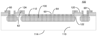
- FIG. 2 illustrates a semiconductor device 100 , semiconductor device 100 comprising: a semiconductor layer 110 exhibiting a first face 112 and a second face 114 opposing first face 112 ; a field layer 120 exhibiting a first face 122 and a second face 124 opposing first face 122 ; and a metal layer 60 exhibiting a first face 62 and a second face 64 opposing first face 62 .
- semiconductor device 100 is a diode.
- semiconductor device 100 is a high voltage diode.
- Semiconductor layer 110 is constituted of a doped material.
- semiconductor layer 110 comprises one of: SiC; silicon; and gallium arsenide (GaAs).
- Semiconductor layer 110 includes at least one doped well 130 .
- semiconductor layer 110 includes a plurality of doped wells 130 .
- Each doped well 130 is doped with a dopant which is of the opposing type of the dopant of semiconductor layer 110 , such that one or more p-n junctions are formed.
- Field layer 120 is constituted of a material having characteristics which effectively block diffusion of mobile ions, i.e. the diffusion coefficient of the material is such that mobile ions will not pass through field layer 120 and reach first face 112 of semiconductor layer 110 .
- the material of field layer 120 has characteristics which effectively block the diffusion of sodium and potassium.
- the material of field layer 120 has characteristics which effectively block the diffusion of all mobile ions.
- the material of field layer 120 has characteristics which effectively blocks the diffusion of mobile ions for at least 1 hour at a temperature of 450 degrees centigrade.
- the material of field layer 120 has characteristics which effectively blocks the diffusion of mobile ions for at least 1000 hours at a temperature of 200 degrees centigrade.
- the material of field layer 120 has characteristics which are sufficiently resistance to polarization and hot carrier injection such that the performance of voltage blocking termination structures does not degrade over reverse bias voltages of up to 1,700 Volts for up to 1,000 hours, at temperatures of up to 175° C.
- the thickness of field layer 120 i.e. the distance between first face 122 and second face 124 , is 0.5-5 micrometers. In one further embodiment, the thickness of field layer 120 is 2-4 micrometers. In another embodiment, the material of field layer 120 has characteristics which effectively block moisture in typical environmental conditions, measured in one embodiment in an 85/85 test.
- the refractive index of field layer 120 is about 1.55-1.60. Particularly, the refractive index provides a measurement of the stoichiometry of field layer 120 .
- a lower refractive index provides increased stability of field layer 110 at high temperatures which allows field layer 120 to maintain structural integrity at activation and assembly temperatures of up to 1,200° C. and 800° C., respectively.
- the stoichiometry of field layer 120 is such that field layer 120 exhibits a graded refractive index.
- the refractive index of field layer 120 increases from first face 122 to second face 124 , i.e. the refractive index of field layer 120 at second face 124 is greater than the refractive index at first face 122 .
- the inventors have discovered that high temperature induced structural deformations in field layers propagate from the interface between the field layer and the semiconductor layer due to the difference in the stoichiometry of the field layer and the semiconductor layer. Therefore, adjusting the stoichiometry of field layer 120 to exhibit a lower refractive index near the semiconductor layer, which is closer to the refractive index of SiO 2 , while exhibiting a higher refractive index at the opposing side thereof, which decreases the diffusivity of field layer 120 , provides a field layer 120 which effectively blocks mobile ions and additionally maintains structural integrity at high temperatures.
- the material of field layer 120 has characteristics which maintain structural integrity at temperatures of up to 800° C. during the assembly process. In one further embodiment, the material of field layer 120 has characteristics which maintain structural integrity at temperatures of up to 1200° C. during the fabrication process.
- field layer 120 is constituted of silicon oxynitride (SiO X N Y ).
- SiO X N Y silicon oxynitride
- the SiO X N Y of field layer 120 has a stoichiometry such that the refractive index at first face 122 is about 1.55 and the refractive index at second face 124 is no more than 1.84. In one further embodiment, the refractive index at second face 124 is about 1.71. In another embodiment, the refractive index at first face 122 is in the range of 1.47-1.49, preferably about 1.48, and the refractive index at second face 124 is between 1.71-1.72. The refractive index increases as the nitrogen content is increased and decreases as the oxygen content is increased. All references to specific refractive indexes in this document are determined with an ellipsometer having a 633 nm light source, it being understood that the specific values are a function of the light source utilized for measurement.
- field layer 120 is constituted of phosphosilicate glass (PSG). In one further embodiment, the PSG exhibits 3%-10% phosphorous within a silicon dioxide matrix. In another embodiment, field layer 120 is constituted of borosilicate glass (BSG). In one further embodiment, the BSG exhibits 3%-10% boric oxide within a silicon dioxide matrix. In one embodiment, field layer 120 is constituted of borophosphosilicate glass (BPSG). In one further embodiment, the BPSG exhibits 3%-10% boric oxide and 3%-10% phosphorous within a silicon dioxide matrix.
- PSG phosphosilicate glass
- BSG borosilicate glass
- BPSG borophosphosilicate glass
- the BPSG exhibits 3%-10% boric oxide and 3%-10% phosphorous within a silicon dioxide matrix.
- First face 122 of field layer 120 faces first face 112 of semiconductor layer 110 , and is patterned thereon, such that field layer 120 is adjacent at least a portion of the at least one doped well 130 .
- field layer 120 covers at least a portion of the at least one doped well 130 .
- field layer 120 is in one embodiment divided into a plurality of sections, each section of field layer 120 covering a respective portion of the at least one doped well 130 .
- the patterning process is performed such that after field layer 120 is patterned on first face 112 of semiconductor layer 110 , field layer 120 exhibits residual film stress, i.e. permanent stress induced by the patterning process, of less than 2 giga-dynes per centimeter squared.
- field layer 120 exhibits residual film stress of less than 1 giga-dyne per centimeter squared.
- First face 62 of metal layer 60 is deposited on at least a portion of first face 112 of semiconductor layer 110 .
- field layer 120 and metal layer 60 together cover the at least one doped well 130 .
- field layer 120 and metal layer 60 together cover the entirety of first face 112 of semiconductor layer 110 .
- first face 62 of metal layer 60 further covers at least a portion of second face 122 of field layer 120 .
- first face 62 of metal layer 60 covers a portion of second face 122 of each part of field layer 120 .
- metal layer 60 is similarly divided into a plurality of sections.
- a passivation layer is not juxtaposed with field layer 120 . Particularly, since field layer 120 blocks mobile ions, no passivation layer is needed.
- FIGS. 3A-3C illustrate steps of an embodiment of a two photomask fabrication process of a FRED.
- a field layer 120 is deposited on a semiconductor layer 20 and a first photomask (not shown) is used to etch field layer 120 .
- field layer 120 is constituted of silicon oxynitride.
- the silicon oxynitride is deposited with a plasma enhanced chemical vapor deposition process, utilizing the Applied Precision 5000 tool, commercially available from Applied Materials of Santa Clara, Calif.
- the following materials were applied at a pressure of 4.2 Torr and at a power of 540 W: silane (SIH 4 ), at a flow rate of 180 sccm; ammonia (NH 3 ), at a flow rate of 35 sccm; nitrous oxide (N 2 O), at a flow rate of 370 sccm; and nitrogen (N 2 ), at a flow rate of 4000 sccm.
- the following materials were applied at a pressure of 4.2 Torr and at a power of 540 W: SIH 4 , at a flow rate of 275 sccm; NH 3 , at a flow rate of 35 sccm; N 2 O, at a flow rate of 180 sccm; and N 2 , at a flow rate of 4000 sccm.
- the patterning process is performed such that after field layer 120 is deposited on semiconductor layer 20 , field layer 120 exhibits residual film stress of less than 2 giga-dynes per centimeter squared. Preferably, field layer 120 exhibits residual film stress of less than 1 giga-dyne per centimeter squared.
- Semiconductor layer 20 comprises: an epitaxial layer 30 exhibiting a first face 32 and a second face 34 , second face 34 opposing first face 32 ; and a doped substrate 40 exhibiting a first face 42 and a second face 44 , second face 44 opposing first face 42 .
- First face 32 of epitaxial layer 30 is deposited on first face 42 of doped substrate 40 and field layer 120 is grown on second face 34 of epitaxial layer 30 .
- field layer 120 exhibits a first face 122 and a second face 124 , second face 124 opposing first face 122 .
- First face 122 of field layer 120 is grown on second face 34 of epitaxial layer 30 .
- dopant ions are implanted into epitaxial layer 30 , through windows 15 , and diffused into the desired depth, to form doped wells 50 .
- the doping of doped wells 50 is the opposite of the doping of semiconductor layer. Particularly, in the event that semiconductor layer 20 is doped with an n-type dopant, doped wells 50 are formed with a p-type dopant, and vice versa.
- the doping level and depth of doped wells 50 are varied dependent upon the desired blocking voltage and the particular voltage blocking scheme.
- Doped wells 50 are activated by annealing epitaxial layer 30 at a high temperature, optionally up to 1200° C.
- a metal layer 60 is deposited onto second face 34 of epitaxial layer 30 and a second photomask (not shown) is used to etch the deposited metal layer 60 to expose portions of field layer 120 .
- metal layer 60 fills in windows 15 to cover doped wells 50 and additionally covers a portion of each of the sections of field layer 120 .
- metal layer 60 comprises: a titanium layer 140 exhibiting a first face 142 and a second face 144 opposing first face 142 ; and an aluminum layer 150 exhibiting a first face 152 and a second face 154 opposing first face 152 .
- first face 142 of titanium layer 140 is deposited onto second face 34 of epitaxial layer 30 and first face 152 of aluminum layer 150 is deposited onto second face 144 of titanium layer 140 .
- Second face 154 of aluminum layer 150 remains exposed and no passivation layer is deposited onto aluminum layer 150 and field layer 120 , as described above.
- FIGS. 4A-4H illustrate steps of an embodiment of a three photomasks fabrication process of an SiC SBD.
- a first step illustrated in FIG. 4A , an oxide layer 200 is deposited on a first face 212 of an SiC wafer 210 and a first photomask (not shown) is used to etch windows 15 into oxide layer 200 .
- dopant ions are implanted into SiC wafer 210 , through windows 15 , to form doped wells 50 .
- the doping of doped wells 50 is the opposite of the doping of semiconductor layer.
- doped wells 50 are formed with a p-type dopant, and vice versa.
- the doping level and depth of doped wells 50 are varied dependent upon the desired blocking voltage and the particular voltage blocking scheme.
- a third step illustrated in FIG.
- etched oxide layer 200 is removed and doped wells 50 are activated by annealing SiC wafer 210 at a high temperature, optionally up to 1,700° C. Prior to the well activation a carbon layer (not shown) is deposited on first face 212 of SiC wafer 210 .
- an oxide layer 220 is deposited on first face 212 of SiC wafer 210 and a nickel layer 230 is deposited on a second face 214 of SiC wafer 210 , second face 214 opposing first face 212 .
- Nickle layer 230 is annealed at a high temperature, optionally up to 1,000° C., to form a nickel silicide layer 240 .
- oxide layer 220 is removed and a field layer 120 is deposited on first face 212 of SiC wafer 210 such that a first face 122 of field layer 120 faces first face 212 of SiC wafer 210 .
- field layer 120 is composed of silicon oxynitride.
- a second photomask (not shown) is used to etch a window 15 into field layer 120 . Depositing field layer 120 only after the activation of doped wells 50 and the formation of nickel silicide layer 240 allows for use of a field layer 120 which does not need to withstand the high annealing temperatures of the well activation and silicide formation.
- the patterning process is performed such that after field layer 120 is deposited on semiconductor layer 210 , field layer 120 exhibits residual film stress of less than 2 giga-dynes per centimeter squared. Preferably, field layer 120 exhibits residual film stress of less than 1 giga-dyne per centimeter squared.
- a metal layer 60 is deposited on a second face 124 of field layer 120 , second face 124 opposing first face 122 thereof. Particularly, metal layer 60 fills in window 15 to cover doped wells 50 and additionally covers etched field layer 120 . Additionally, a third photomask (not shown) is used to etch metal layer 60 to expose portions of etched field layer 120 .
- metal layer 60 comprises: a titanium layer 140 exhibiting a first face 142 and a second face 144 opposing first face 142 ; and an aluminum layer 150 exhibiting a first face 152 and a second face 154 opposing first face 152 .
- first face 142 of titanium layer 140 is deposited onto first face 212 of SiC wafer 210 and first face 152 of aluminum layer 150 is deposited onto second face 144 of titanium layer 140 .
- Second face 154 of aluminum layer 150 remains exposed and no passivation layer is deposited onto aluminum layer 150 and field layer 120 , as described above.
- a metal layer 250 is deposited on nickel silicide layer 240 .
- an oxide layer (not shown) is deposited on nickel silicide layer 240 , annealed at a temperature of about 450° C. and removed.
- FIG. 5 illustrates a high level flow chart of a semiconductor device fabrication method, in accordance with certain embodiments.
- a field layer is patterned on a first face of a semiconductor layer.
- the field layer is constituted of material having characteristics which block diffusion of mobile ions, and which maintains structural integrity at processing temperatures up to 1200° C.
- the field layer material characteristics block the diffusion of mobile ions for at least 1 hour at a temperature of 450 degrees centigrade.
- the field layer material characteristics block the diffusion of mobile ions for at least 1000 hours at a temperature of 200 degrees centigrade.
- the patterned field layer exhibits residual film stress of less than 2 giga-dynes per centimeter squared.
- the patterned field layer exhibits residual film stress of less than 1 giga-dyne per centimeter squared.
- the material of the field layer has characteristics which are sufficiently resistant to polarization and hot carrier injection such that the performance of voltage blocking termination structures does not degrade over reverse bias voltages of up to 1,700 Volts for up to 1,000 hours, at temperatures of up to 175° C.
- the field layer exhibits a first face and a second face opposing the first face thereof, the field layer being patterned such that the first face thereof faces the first face of the semiconductor layer. Additionally, the refractive index of the field layer increases from the first face to the second face thereof, i.e. the refractive index of the field layer at the second face thereof is greater than the refractive index of the field layer at the first face thereof.
- the material characteristics of the field layer block moisture.
- the material of the patterned layer is selected from the group consisting of: silicon oxynitride; phosphosilicate glass; borosilicate glass; and borophosphosilicate glass.
- At least one doped well is formed within the semiconductor layer.
- the patterning of stage 1000 is arranged such that the patterned field layer is adjacent at least a portion of at least one doped well.
- the at least one doped well of optional stage 1010 is activated.
- the doped well activation is performed by annealing the semiconductor layer of stage 1000 at a high temperature.
- a silicide layer is formed on a second face of the semiconductor layer of stage 1000 . The second face of the semiconductor layer opposes the first face thereof.
- the patterning of stage 1000 is performed after: the implantation of the at least one doped wells of stage optional stage 1010 ; the activation of the at least one doped wells of optional stage 1020 ; and the formation of the silicide layer.
- the steps of optional stages 1010 - 1030 are all high temperature processes, and the field layer material characteristics maintain structural integrity at the processing temperatures of up to 1200° C. Patterning the field layer after the high temperature processes are completed prevents cracking of the field layer.
- a metal layer is deposited on at least a portion of the first face of the semiconductor layer of stage 1000 . The patterned field layer and the deposited metal layer completely cover the at least one doped well of optional stage 1010 .
- a low contact resistance backside metal is deposited on the second face of the semiconductor layer of stage 1000
Landscapes
- Engineering & Computer Science (AREA)
- Microelectronics & Electronic Packaging (AREA)
- Power Engineering (AREA)
- Physics & Mathematics (AREA)
- Computer Hardware Design (AREA)
- Condensed Matter Physics & Semiconductors (AREA)
- General Physics & Mathematics (AREA)
- Manufacturing & Machinery (AREA)
- Ceramic Engineering (AREA)
- Chemical & Material Sciences (AREA)
- Crystallography & Structural Chemistry (AREA)
- High Energy & Nuclear Physics (AREA)
- Plasma & Fusion (AREA)
- Chemical Kinetics & Catalysis (AREA)
- Health & Medical Sciences (AREA)
- Toxicology (AREA)
- Electrodes Of Semiconductors (AREA)
Abstract
Description
D=D 0 *e −E
where D0 is the maximal diffusion coefficient, EA is the diffusion activation energy, k is the Boltzmann constant and T is the absolute temperature. As shown in EQ. 1, the diffusion coefficient is an exponential function of the temperature.
Claims (23)
Priority Applications (1)
| Application Number | Priority Date | Filing Date | Title |
|---|---|---|---|
| US16/103,949 US10566416B2 (en) | 2017-08-21 | 2018-08-15 | Semiconductor device with improved field layer |
Applications Claiming Priority (2)
| Application Number | Priority Date | Filing Date | Title |
|---|---|---|---|
| US201762547901P | 2017-08-21 | 2017-08-21 | |
| US16/103,949 US10566416B2 (en) | 2017-08-21 | 2018-08-15 | Semiconductor device with improved field layer |
Publications (2)
| Publication Number | Publication Date |
|---|---|
| US20190058032A1 US20190058032A1 (en) | 2019-02-21 |
| US10566416B2 true US10566416B2 (en) | 2020-02-18 |
Family
ID=65360769
Family Applications (1)
| Application Number | Title | Priority Date | Filing Date |
|---|---|---|---|
| US16/103,949 Active US10566416B2 (en) | 2017-08-21 | 2018-08-15 | Semiconductor device with improved field layer |
Country Status (1)
| Country | Link |
|---|---|
| US (1) | US10566416B2 (en) |
Citations (6)
| Publication number | Priority date | Publication date | Assignee | Title |
|---|---|---|---|---|
| US5674788A (en) | 1995-06-06 | 1997-10-07 | Advanced Micro Devices, Inc. | Method of forming high pressure silicon oxynitride gate dielectrics |
| US20020130371A1 (en) * | 2001-03-19 | 2002-09-19 | Bryant Frank R. | Printhead integrated circuit |
| US6930060B2 (en) | 2003-06-18 | 2005-08-16 | International Business Machines Corporation | Method for forming a uniform distribution of nitrogen in silicon oxynitride gate dielectric |
| US6936905B2 (en) | 2003-04-24 | 2005-08-30 | Shye-Lin Wu | Two mask shottky diode with locos structure |
| US7671410B2 (en) | 2003-01-15 | 2010-03-02 | Microsemi Corporation | Design and fabrication of rugged FRED, power MOSFET or IGBT |
| US8110888B2 (en) | 2007-09-18 | 2012-02-07 | Microsemi Corporation | Edge termination for high voltage semiconductor device |
-
2018
- 2018-08-15 US US16/103,949 patent/US10566416B2/en active Active
Patent Citations (6)
| Publication number | Priority date | Publication date | Assignee | Title |
|---|---|---|---|---|
| US5674788A (en) | 1995-06-06 | 1997-10-07 | Advanced Micro Devices, Inc. | Method of forming high pressure silicon oxynitride gate dielectrics |
| US20020130371A1 (en) * | 2001-03-19 | 2002-09-19 | Bryant Frank R. | Printhead integrated circuit |
| US7671410B2 (en) | 2003-01-15 | 2010-03-02 | Microsemi Corporation | Design and fabrication of rugged FRED, power MOSFET or IGBT |
| US6936905B2 (en) | 2003-04-24 | 2005-08-30 | Shye-Lin Wu | Two mask shottky diode with locos structure |
| US6930060B2 (en) | 2003-06-18 | 2005-08-16 | International Business Machines Corporation | Method for forming a uniform distribution of nitrogen in silicon oxynitride gate dielectric |
| US8110888B2 (en) | 2007-09-18 | 2012-02-07 | Microsemi Corporation | Edge termination for high voltage semiconductor device |
Also Published As
| Publication number | Publication date |
|---|---|
| US20190058032A1 (en) | 2019-02-21 |
Similar Documents
| Publication | Publication Date | Title |
|---|---|---|
| US8003991B2 (en) | Silicon carbide MOS field effect transistor with built-in Schottky diode and method for fabrication thereof | |
| CA1259530A (en) | Silicon oxynitride passivated semiconductor device and method of making same | |
| JP3940560B2 (en) | Manufacturing method of semiconductor device | |
| US10304972B2 (en) | Solar cell with silicon oxynitride dielectric layer | |
| US20090288704A1 (en) | Nitrided barrier layers for solar cells | |
| US20060108589A1 (en) | Semiconductor device | |
| US20100186803A1 (en) | Buried insulator isolation for solar cell contacts | |
| US7170044B2 (en) | Semiconductor photodetector for detecting light having a wavelength in the ultraviolet blue ranges | |
| DK142758B (en) | Semiconductor element with passivation layer. | |
| US9911873B2 (en) | Hydrogenation of passivated contacts | |
| US4161744A (en) | Passivated semiconductor device and method of making same | |
| US20070096107A1 (en) | Semiconductor devices with dielectric layers and methods of fabricating same | |
| US10566416B2 (en) | Semiconductor device with improved field layer | |
| US20100308340A1 (en) | Semiconductor device having a buried channel | |
| US9331142B2 (en) | Zener diode having a polysilicon layer for improved reverse surge capability and decreased leakage current | |
| KR101665863B1 (en) | Rectifier diode and method of fabricating the same | |
| Garafalo | The Cleaning and Passivation of Germanium X-ray Photodiodes | |
| JPS6052580B2 (en) | Manufacturing method for surface protective film in semiconductor devices | |
| Nemeth et al. | Hydrogenation of passivated contacts | |
| TWI557925B (en) | Semiconductor device and method of manufacturing the same | |
| Damnjanović et al. | Electrical characteristics of HgCdTe Schottky diode photo-detectors with passivation layers transparent to free carriers | |
| JPS62204519A (en) | Substrate structure for silicon carbide device | |
| Ambrosio et al. | Optimization of the contact resistance in the interface structure of n‐type Al/a‐SiC: H by thermal annealing for optoelectronics applications | |
| JPH07202181A (en) | Mosfet with gate insulating film protection diode and manufacture of mosfet interlayer insulating film | |
| JPS5848478A (en) | Forming method of inp diode in which be is implanted |
Legal Events
| Date | Code | Title | Description |
|---|---|---|---|
| FEPP | Fee payment procedure |
Free format text: ENTITY STATUS SET TO UNDISCOUNTED (ORIGINAL EVENT CODE: BIG.); ENTITY STATUS OF PATENT OWNER: LARGE ENTITY |
|
| AS | Assignment |
Owner name: MICROSEMI CORPORATION, CALIFORNIA Free format text: ASSIGNMENT OF ASSIGNORS INTEREST;ASSIGNORS:GENDRON-HANSEN, AMAURY;ODEKIRK, BRUCE;BERLINER, NATHANIEL;AND OTHERS;SIGNING DATES FROM 20180813 TO 20180814;REEL/FRAME:046786/0917 |
|
| STPP | Information on status: patent application and granting procedure in general |
Free format text: DOCKETED NEW CASE - READY FOR EXAMINATION |
|
| STPP | Information on status: patent application and granting procedure in general |
Free format text: NON FINAL ACTION MAILED |
|
| STPP | Information on status: patent application and granting procedure in general |
Free format text: RESPONSE TO NON-FINAL OFFICE ACTION ENTERED AND FORWARDED TO EXAMINER |
|
| STPP | Information on status: patent application and granting procedure in general |
Free format text: NOTICE OF ALLOWANCE MAILED -- APPLICATION RECEIVED IN OFFICE OF PUBLICATIONS |
|
| STPP | Information on status: patent application and granting procedure in general |
Free format text: PUBLICATIONS -- ISSUE FEE PAYMENT RECEIVED |
|
| STCF | Information on status: patent grant |
Free format text: PATENTED CASE |
|
| AS | Assignment |
Owner name: JPMORGAN CHASE BANK, N.A., AS ADMINISTRATIVE AGENT, DELAWARE Free format text: SECURITY INTEREST;ASSIGNORS:MICROCHIP TECHNOLOGY INC.;SILICON STORAGE TECHNOLOGY, INC.;ATMEL CORPORATION;AND OTHERS;REEL/FRAME:053311/0305 Effective date: 20200327 |
|
| AS | Assignment |
Owner name: MICROSEMI CORPORATION, CALIFORNIA Free format text: RELEASE BY SECURED PARTY;ASSIGNOR:JPMORGAN CHASE BANK, N.A, AS ADMINISTRATIVE AGENT;REEL/FRAME:053466/0011 Effective date: 20200529 Owner name: MICROSEMI STORAGE SOLUTIONS, INC., ARIZONA Free format text: RELEASE BY SECURED PARTY;ASSIGNOR:JPMORGAN CHASE BANK, N.A, AS ADMINISTRATIVE AGENT;REEL/FRAME:053466/0011 Effective date: 20200529 Owner name: SILICON STORAGE TECHNOLOGY, INC., ARIZONA Free format text: RELEASE BY SECURED PARTY;ASSIGNOR:JPMORGAN CHASE BANK, N.A, AS ADMINISTRATIVE AGENT;REEL/FRAME:053466/0011 Effective date: 20200529 Owner name: ATMEL CORPORATION, ARIZONA Free format text: RELEASE BY SECURED PARTY;ASSIGNOR:JPMORGAN CHASE BANK, N.A, AS ADMINISTRATIVE AGENT;REEL/FRAME:053466/0011 Effective date: 20200529 Owner name: MICROCHIP TECHNOLOGY INC., ARIZONA Free format text: RELEASE BY SECURED PARTY;ASSIGNOR:JPMORGAN CHASE BANK, N.A, AS ADMINISTRATIVE AGENT;REEL/FRAME:053466/0011 Effective date: 20200529 |
|
| AS | Assignment |
Owner name: JPMORGAN CHASE BANK, N.A., AS ADMINISTRATIVE AGENT, ILLINOIS Free format text: SECURITY INTEREST;ASSIGNORS:MICROCHIP TECHNOLOGY INC.;SILICON STORAGE TECHNOLOGY, INC.;ATMEL CORPORATION;AND OTHERS;REEL/FRAME:052856/0909 Effective date: 20200529 Owner name: WELLS FARGO BANK, NATIONAL ASSOCIATION, MINNESOTA Free format text: SECURITY INTEREST;ASSIGNORS:MICROCHIP TECHNOLOGY INC.;SILICON STORAGE TECHNOLOGY, INC.;ATMEL CORPORATION;AND OTHERS;REEL/FRAME:053468/0705 Effective date: 20200529 |
|
| AS | Assignment |
Owner name: WELLS FARGO BANK, NATIONAL ASSOCIATION, AS COLLATERAL AGENT, MINNESOTA Free format text: SECURITY INTEREST;ASSIGNORS:MICROCHIP TECHNOLOGY INCORPORATED;SILICON STORAGE TECHNOLOGY, INC.;ATMEL CORPORATION;AND OTHERS;REEL/FRAME:055671/0612 Effective date: 20201217 |
|
| AS | Assignment |
Owner name: WELLS FARGO BANK, NATIONAL ASSOCIATION, AS NOTES COLLATERAL AGENT, MINNESOTA Free format text: SECURITY INTEREST;ASSIGNORS:MICROCHIP TECHNOLOGY INCORPORATED;SILICON STORAGE TECHNOLOGY, INC.;ATMEL CORPORATION;AND OTHERS;REEL/FRAME:057935/0474 Effective date: 20210528 |
|
| AS | Assignment |
Owner name: WELLS FARGO BANK, NATIONAL ASSOCIATION, AS NOTES COLLATERAL AGENT, MINNESOTA Free format text: GRANT OF SECURITY INTEREST IN PATENT RIGHTS;ASSIGNORS:MICROCHIP TECHNOLOGY INCORPORATED;SILICON STORAGE TECHNOLOGY, INC.;ATMEL CORPORATION;AND OTHERS;REEL/FRAME:058214/0625 Effective date: 20211117 |
|
| AS | Assignment |
Owner name: MICROSEMI STORAGE SOLUTIONS, INC., ARIZONA Free format text: RELEASE BY SECURED PARTY;ASSIGNOR:JPMORGAN CHASE BANK, N.A., AS ADMINISTRATIVE AGENT;REEL/FRAME:059263/0001 Effective date: 20220218 Owner name: MICROSEMI CORPORATION, ARIZONA Free format text: RELEASE BY SECURED PARTY;ASSIGNOR:JPMORGAN CHASE BANK, N.A., AS ADMINISTRATIVE AGENT;REEL/FRAME:059263/0001 Effective date: 20220218 Owner name: ATMEL CORPORATION, ARIZONA Free format text: RELEASE BY SECURED PARTY;ASSIGNOR:JPMORGAN CHASE BANK, N.A., AS ADMINISTRATIVE AGENT;REEL/FRAME:059263/0001 Effective date: 20220218 Owner name: SILICON STORAGE TECHNOLOGY, INC., ARIZONA Free format text: RELEASE BY SECURED PARTY;ASSIGNOR:JPMORGAN CHASE BANK, N.A., AS ADMINISTRATIVE AGENT;REEL/FRAME:059263/0001 Effective date: 20220218 Owner name: MICROCHIP TECHNOLOGY INCORPORATED, ARIZONA Free format text: RELEASE BY SECURED PARTY;ASSIGNOR:JPMORGAN CHASE BANK, N.A., AS ADMINISTRATIVE AGENT;REEL/FRAME:059263/0001 Effective date: 20220218 |
|
| AS | Assignment |
Owner name: MICROSEMI STORAGE SOLUTIONS, INC., ARIZONA Free format text: RELEASE BY SECURED PARTY;ASSIGNOR:WELLS FARGO BANK, NATIONAL ASSOCIATION, AS NOTES COLLATERAL AGENT;REEL/FRAME:059358/0335 Effective date: 20220228 Owner name: MICROSEMI CORPORATION, ARIZONA Free format text: RELEASE BY SECURED PARTY;ASSIGNOR:WELLS FARGO BANK, NATIONAL ASSOCIATION, AS NOTES COLLATERAL AGENT;REEL/FRAME:059358/0335 Effective date: 20220228 Owner name: ATMEL CORPORATION, ARIZONA Free format text: RELEASE BY SECURED PARTY;ASSIGNOR:WELLS FARGO BANK, NATIONAL ASSOCIATION, AS NOTES COLLATERAL AGENT;REEL/FRAME:059358/0335 Effective date: 20220228 Owner name: SILICON STORAGE TECHNOLOGY, INC., ARIZONA Free format text: RELEASE BY SECURED PARTY;ASSIGNOR:WELLS FARGO BANK, NATIONAL ASSOCIATION, AS NOTES COLLATERAL AGENT;REEL/FRAME:059358/0335 Effective date: 20220228 Owner name: MICROCHIP TECHNOLOGY INCORPORATED, ARIZONA Free format text: RELEASE BY SECURED PARTY;ASSIGNOR:WELLS FARGO BANK, NATIONAL ASSOCIATION, AS NOTES COLLATERAL AGENT;REEL/FRAME:059358/0335 Effective date: 20220228 |
|
| AS | Assignment |
Owner name: MICROSEMI STORAGE SOLUTIONS, INC., ARIZONA Free format text: RELEASE BY SECURED PARTY;ASSIGNOR:WELLS FARGO BANK, NATIONAL ASSOCIATION, AS NOTES COLLATERAL AGENT;REEL/FRAME:059863/0400 Effective date: 20220228 Owner name: MICROSEMI CORPORATION, ARIZONA Free format text: RELEASE BY SECURED PARTY;ASSIGNOR:WELLS FARGO BANK, NATIONAL ASSOCIATION, AS NOTES COLLATERAL AGENT;REEL/FRAME:059863/0400 Effective date: 20220228 Owner name: ATMEL CORPORATION, ARIZONA Free format text: RELEASE BY SECURED PARTY;ASSIGNOR:WELLS FARGO BANK, NATIONAL ASSOCIATION, AS NOTES COLLATERAL AGENT;REEL/FRAME:059863/0400 Effective date: 20220228 Owner name: SILICON STORAGE TECHNOLOGY, INC., ARIZONA Free format text: RELEASE BY SECURED PARTY;ASSIGNOR:WELLS FARGO BANK, NATIONAL ASSOCIATION, AS NOTES COLLATERAL AGENT;REEL/FRAME:059863/0400 Effective date: 20220228 Owner name: MICROCHIP TECHNOLOGY INCORPORATED, ARIZONA Free format text: RELEASE BY SECURED PARTY;ASSIGNOR:WELLS FARGO BANK, NATIONAL ASSOCIATION, AS NOTES COLLATERAL AGENT;REEL/FRAME:059863/0400 Effective date: 20220228 |
|
| AS | Assignment |
Owner name: MICROSEMI STORAGE SOLUTIONS, INC., ARIZONA Free format text: RELEASE BY SECURED PARTY;ASSIGNOR:WELLS FARGO BANK, NATIONAL ASSOCIATION, AS NOTES COLLATERAL AGENT;REEL/FRAME:059363/0001 Effective date: 20220228 Owner name: MICROSEMI CORPORATION, ARIZONA Free format text: RELEASE BY SECURED PARTY;ASSIGNOR:WELLS FARGO BANK, NATIONAL ASSOCIATION, AS NOTES COLLATERAL AGENT;REEL/FRAME:059363/0001 Effective date: 20220228 Owner name: ATMEL CORPORATION, ARIZONA Free format text: RELEASE BY SECURED PARTY;ASSIGNOR:WELLS FARGO BANK, NATIONAL ASSOCIATION, AS NOTES COLLATERAL AGENT;REEL/FRAME:059363/0001 Effective date: 20220228 Owner name: SILICON STORAGE TECHNOLOGY, INC., ARIZONA Free format text: RELEASE BY SECURED PARTY;ASSIGNOR:WELLS FARGO BANK, NATIONAL ASSOCIATION, AS NOTES COLLATERAL AGENT;REEL/FRAME:059363/0001 Effective date: 20220228 Owner name: MICROCHIP TECHNOLOGY INCORPORATED, ARIZONA Free format text: RELEASE BY SECURED PARTY;ASSIGNOR:WELLS FARGO BANK, NATIONAL ASSOCIATION, AS NOTES COLLATERAL AGENT;REEL/FRAME:059363/0001 Effective date: 20220228 |
|
| AS | Assignment |
Owner name: MICROSEMI STORAGE SOLUTIONS, INC., ARIZONA Free format text: RELEASE BY SECURED PARTY;ASSIGNOR:WELLS FARGO BANK, NATIONAL ASSOCIATION, AS NOTES COLLATERAL AGENT;REEL/FRAME:060894/0437 Effective date: 20220228 Owner name: MICROSEMI CORPORATION, ARIZONA Free format text: RELEASE BY SECURED PARTY;ASSIGNOR:WELLS FARGO BANK, NATIONAL ASSOCIATION, AS NOTES COLLATERAL AGENT;REEL/FRAME:060894/0437 Effective date: 20220228 Owner name: ATMEL CORPORATION, ARIZONA Free format text: RELEASE BY SECURED PARTY;ASSIGNOR:WELLS FARGO BANK, NATIONAL ASSOCIATION, AS NOTES COLLATERAL AGENT;REEL/FRAME:060894/0437 Effective date: 20220228 Owner name: SILICON STORAGE TECHNOLOGY, INC., ARIZONA Free format text: RELEASE BY SECURED PARTY;ASSIGNOR:WELLS FARGO BANK, NATIONAL ASSOCIATION, AS NOTES COLLATERAL AGENT;REEL/FRAME:060894/0437 Effective date: 20220228 Owner name: MICROCHIP TECHNOLOGY INCORPORATED, ARIZONA Free format text: RELEASE BY SECURED PARTY;ASSIGNOR:WELLS FARGO BANK, NATIONAL ASSOCIATION, AS NOTES COLLATERAL AGENT;REEL/FRAME:060894/0437 Effective date: 20220228 |
|
| MAFP | Maintenance fee payment |
Free format text: PAYMENT OF MAINTENANCE FEE, 4TH YEAR, LARGE ENTITY (ORIGINAL EVENT CODE: M1551); ENTITY STATUS OF PATENT OWNER: LARGE ENTITY Year of fee payment: 4 |