EP0056084A1 - Elektrostatisch ablenkbare Schalter - Google Patents
Elektrostatisch ablenkbare Schalter Download PDFInfo
- Publication number
- EP0056084A1 EP0056084A1 EP81108117A EP81108117A EP0056084A1 EP 0056084 A1 EP0056084 A1 EP 0056084A1 EP 81108117 A EP81108117 A EP 81108117A EP 81108117 A EP81108117 A EP 81108117A EP 0056084 A1 EP0056084 A1 EP 0056084A1
- Authority
- EP
- European Patent Office
- Prior art keywords
- electrode
- insulating material
- electrodes
- voltage
- layer
- Prior art date
- Legal status (The legal status is an assumption and is not a legal conclusion. Google has not performed a legal analysis and makes no representation as to the accuracy of the status listed.)
- Granted
Links
- 239000000758 substrate Substances 0.000 claims abstract description 15
- 239000011810 insulating material Substances 0.000 claims description 14
- 229910052751 metal Inorganic materials 0.000 claims description 9
- 239000002184 metal Substances 0.000 claims description 9
- 229910052710 silicon Inorganic materials 0.000 claims description 8
- 239000010703 silicon Substances 0.000 claims description 8
- 238000005452 bending Methods 0.000 claims description 7
- 239000000463 material Substances 0.000 claims description 5
- VYPSYNLAJGMNEJ-UHFFFAOYSA-N Silicium dioxide Chemical compound O=[Si]=O VYPSYNLAJGMNEJ-UHFFFAOYSA-N 0.000 claims description 3
- 239000011248 coating agent Substances 0.000 claims 9
- 238000000576 coating method Methods 0.000 claims 9
- 235000012239 silicon dioxide Nutrition 0.000 claims 1
- 239000000377 silicon dioxide Substances 0.000 claims 1
- 239000010409 thin film Substances 0.000 claims 1
- 230000003287 optical effect Effects 0.000 abstract description 10
- 230000009977 dual effect Effects 0.000 abstract description 2
- XUIMIQQOPSSXEZ-UHFFFAOYSA-N Silicon Chemical compound [Si] XUIMIQQOPSSXEZ-UHFFFAOYSA-N 0.000 description 7
- 230000001133 acceleration Effects 0.000 description 6
- 238000009792 diffusion process Methods 0.000 description 5
- 239000004065 semiconductor Substances 0.000 description 5
- 238000013461 design Methods 0.000 description 4
- 230000002457 bidirectional effect Effects 0.000 description 3
- ZOXJGFHDIHLPTG-UHFFFAOYSA-N Boron Chemical compound [B] ZOXJGFHDIHLPTG-UHFFFAOYSA-N 0.000 description 2
- 229910052782 aluminium Inorganic materials 0.000 description 2
- XAGFODPZIPBFFR-UHFFFAOYSA-N aluminium Chemical compound [Al] XAGFODPZIPBFFR-UHFFFAOYSA-N 0.000 description 2
- 238000003491 array Methods 0.000 description 2
- 229910052796 boron Inorganic materials 0.000 description 2
- 238000010276 construction Methods 0.000 description 2
- 238000010894 electron beam technology Methods 0.000 description 2
- 238000005530 etching Methods 0.000 description 2
- 230000006870 function Effects 0.000 description 2
- 239000012528 membrane Substances 0.000 description 2
- 230000015572 biosynthetic process Effects 0.000 description 1
- 239000003990 capacitor Substances 0.000 description 1
- 238000001514 detection method Methods 0.000 description 1
- 230000000694 effects Effects 0.000 description 1
- 239000011888 foil Substances 0.000 description 1
- 230000005484 gravity Effects 0.000 description 1
- 239000011159 matrix material Substances 0.000 description 1
- 238000000034 method Methods 0.000 description 1
- 230000000737 periodic effect Effects 0.000 description 1
- 238000012545 processing Methods 0.000 description 1
- 238000012827 research and development Methods 0.000 description 1
- 229910052814 silicon oxide Inorganic materials 0.000 description 1
- 239000012780 transparent material Substances 0.000 description 1
Images


Classifications
-
- G—PHYSICS
- G09—EDUCATION; CRYPTOGRAPHY; DISPLAY; ADVERTISING; SEALS
- G09F—DISPLAYING; ADVERTISING; SIGNS; LABELS OR NAME-PLATES; SEALS
- G09F9/00—Indicating arrangements for variable information in which the information is built-up on a support by selection or combination of individual elements
- G09F9/30—Indicating arrangements for variable information in which the information is built-up on a support by selection or combination of individual elements in which the desired character or characters are formed by combining individual elements
- G09F9/37—Indicating arrangements for variable information in which the information is built-up on a support by selection or combination of individual elements in which the desired character or characters are formed by combining individual elements being movable elements
- G09F9/372—Indicating arrangements for variable information in which the information is built-up on a support by selection or combination of individual elements in which the desired character or characters are formed by combining individual elements being movable elements the positions of the elements being controlled by the application of an electric field
-
- G—PHYSICS
- G11—INFORMATION STORAGE
- G11C—STATIC STORES
- G11C11/00—Digital stores characterised by the use of particular electric or magnetic storage elements; Storage elements therefor
-
- G—PHYSICS
- G11—INFORMATION STORAGE
- G11C—STATIC STORES
- G11C13/00—Digital stores characterised by the use of storage elements not covered by groups G11C11/00, G11C23/00, or G11C25/00
- G11C13/04—Digital stores characterised by the use of storage elements not covered by groups G11C11/00, G11C23/00, or G11C25/00 using optical elements ; using other beam accessed elements, e.g. electron or ion beam
-
- H—ELECTRICITY
- H01—ELECTRIC ELEMENTS
- H01H—ELECTRIC SWITCHES; RELAYS; SELECTORS; EMERGENCY PROTECTIVE DEVICES
- H01H59/00—Electrostatic relays; Electro-adhesion relays
- H01H59/0009—Electrostatic relays; Electro-adhesion relays making use of micromechanics
Definitions
- This invention relates to electrostatically deflectable light switches used in deformographic displays and more particularly to an improved switch which can be driven by co-incident voltages.
- Electrostatically deflectable light valves are shown in U.S. Patent 3 746 911 to H.C. Nathanson, et al; U.S. Patent 3 886 310 to J. Guldberg et al; U.S. Patent 3 989 890 to H.C. Nathanson, et al; and described in an article entitled "The Mirror-Matrix Tube: A Novel Light Valve for Projection Displays” authored by R. N. Thomas et al, which appeared in the "IEEE Transactions on Electron Devices", Vol. ED-22, 9. Sept. 1975, on pp. 765-775.
- the deflectable light valve described in this paper and the above patents requires an electron beam drive and thus a surrounding vacuum atmosphere.
- U.S. Patent 3,137,762 to W. Baumgartner et al discloses a device for amplifying the brightness of an optical image.
- the invention as claimed is intendend to remedy the drawback mentioned above and to improve known devices. It solves the problem of how to design an electrostatically deformographic switching device driven by coincident voltages and is especially useful in an array since it can be used as either a display or a memory.
- the advantage offered by the invention is mainly that a direct drive display is available which does not need either vacuum envelopes or electron beam drives. Furthermore, greater efficiencies can be realized and no refresh is necessary since the switch will operate in a standby condition. Also only two voltage levels above ground, i.e., a write voltage and a standby voltage, are required. The switch will enable copiers to be directly driven by computers.
- the switch can also be used as an optical waveguide transmit/receive switch or an accelerometer.
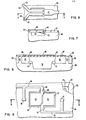
- Figure 1 illustrates a partically cross-sectioned, pictorial view of the preferred embodiment of the invention in which the localized stress due to the electrostatic force on the beam is modified by formation of an interdigitated electrode structure on the surface of the beam.
- the embodiment shown comprises a body 10 of semiconductor material, such as silicon, having a layer of insulating material, such as silicon oxide, on one surface thereof.
- a cantilevered beam 12 of this oxide material is formed by cutting a U-shaped trench in the oxide and etching a pit in the silicon body beneath the beam 12.
- Figure 2 illustrates a sectional view of the device of Figure 1 during one stage of its construction.
- the body 10 is comprised of a p-type substrate 16 having an epitaxial layer 17 formed thereon with a p+ type region 18, doped with boron to a concentration peak exceeding typically 7x10 19 , disposed between the epitaxial layer 17 and the substrate 16.
- Another p-type region 19 is formed in the epitaxial layer 17 through an opening 20 in the oxide layer 11. Once the region 19 is formed so that it extends down from the surface of the epitaxial layer 17 to merge with the p-type region 13, an oxide lla is regrown in the opening 20. This regrown layer lla is considerably thinner than the original oxide 11 because of the methods used to regrow such oxides.
- a U-shaped trench 21 is formed in the oxide layer 11 overlying the p-type region 18 with the open end of the U enclosing the region 19.
- This U-shaped etch defines the oxide beam 12.
- the pit 13 is formed by introducing a.selective anisotropic etchant through the opening 21 so that the silicon body 11 is etched away beneath the beam 12 leaving it in a cantilevered position over the pit 13. Boron to the described concentration levels is used to limit the amount of vertical etching when anistropic etchants are used.
- a metal for forming the electrodes 14 and 15 is then deposited over the surface of the beam and the interdigitated electrodes 14 and 15 defined therein.
- this regrown oxide layer lla is substantially thinner than the oxide covering the beam 12, it acts as a hinge when the pit 13 extends under it and helps to lower the stress when the beam is deflected under the influence of an electrostatic force developed by biasing the electrodes 14 and 15 with respect to the underlying P region 18.
- the beam 12 experiences no deflection.
- the threshold voltage a critical level called the threshold voltage.
- the electrostatic forces overcome the internal forces of the beam and the beam suddenly snaps down into a fully deflected position whith the end of the beam touching the bottom of the pit. Because the beam is formed of an insulating material the electrodes are prevented from touching the bottom of the pit.
- the voltage can be reduced below threshold and still maintain the beam in its deflected position. Indeed, before the beam will return to its initial undeflected position, after having been put into a fully deflected position, the applied voltage must fall below a minimum holding voltage which is nearly zero volts. This minimum holding voltage is that voltage at which the electrostatic force falls below the level of the internal stresses in the deflected beam. When this minimum holding is reached the beam will suddenly snap back to its initial zero position.
- the position of the beam can be used to store information.
- the deflected beam can be a "1" and the undeflected beam a "0".
- the position of the beam is determined by impinging a ray of light,normal to the undeflected surface of the beam and placing an optical detector normal to the fully deflected position of the beam.
- the ray of light is reflected back to its source and the detector is dark and thus can represent a zero.
- the beam is fully deflected and the ray of light impinges on the deflected end it is reflected, from the beam at an angle to its original path, and becomes diverted toward the detector. This detected beam can represent a "1".
- the voltage applied to both electrodes must be equal to the threshold level before the beam will fully deflect. If two different voltages are applied and one is below the threshold level while the other is at the threshold level the beam will not fully deflect.
- the beam is fully deflected
- the voltages on both of the electrodes could be reduced to one-half the threshold voltage and still cause the beam to remain in its deflected position.
- the threshold for the case where Vy is greater than Vx is smaller than the case where Vy is less than Vx. Since the end most element of the electrode at the distant end, or tip of the beam, is element 15, i. e., Vy produces the greatest force on the beam and thus the most bending movement because for any given voltage the force on the beam is proportional to the square of the reciprocal distance between the electrodes. This basically says that the minimum holding force on the beam required to keep it in a fully deflected position is a complex function of the voltages of both electrodes and that the voltage should never go to zero but should always be at a standby voltage, somewhat in excess of zero. This standby voltage should be for example about one-half the threshold voltage.
- Vx does not have to be brought to ground to cause the device to switch back to its undeflected position.
- Vx need only be at threshold or one-half threshold while the other line is tri-state threshold to deflect the device, one-half threshold to hold it fully deflected if previously fully deflected and zero volts to permit the beam to return from a fully deflected position to an undeflected position.
- This arrangement of interdigitated electrodes now gives the capability of easily forming an x-y array in any size in which each device can readily and easily be written into and held in a deflected state.
- the present invention results in an array that can be used as a memory or storage which is twice as dense as was the prior art arrays and which can easily be written with two co-incident voltages, i. e., one applied to electrode 14 and the other applied to electrode 15. Also only two voltage levels, i. e., one-half threshold and threshold, above ground or zero volts are required.
- Such a reduction in deflection force is also realized by either producing an opening in the beam or by narrowing of the beam at its proximal end, i. e., its juncture with the main oxide layer. Such opening or narrowing reduces the movement of inertia of the beam, thus reducing the level of the necessary deflecting force and the required threshold voltage.
- FIG. 4 depicts a semiconductor body 40 having an oxide layer 41 on the surface thereof. Formed in this oxide layer 41 is a substantially square oxide beam 44 suspended over an etched pit 46 provided in the body 40, by a hinge 45 located on one corner of the beam. The other three corners of the beam are freely cantilevered over the pit 46.
- Two interdigitated electrodes 42 and 43 are disposed over the beam 44. The electrode 42 is substantially enclosed by the electrode 43. The electrodes 42 and 43 are separated one from the other, over the beam, by a space 47.
- This electrostatic deformographic device operates in the same manner as does the device shown in Figure 1. However, in this case the corner 48 of the beam, which is diagonally opposite the hinge 45, is the point of greatest deflection when voltages above the threshold voltage are applied to the electrodes 42 and 43.
- this corner deflectable device has a distinct advantage over that shown in Figure 1.
- Figure 5 depicts still another embodiment.
- the device shown in Figure 5 is substantially the same as the device shown in Figure 4.
- This semiconductor body 50 is covered with an oxide layer 51 which was defined therein a substantially square oxide beam 54 suspended by a'corner hinge 55 over a pit 56 etched in the body 50.
- a first substantially square electrode 52 is disposed over the center of the beam 54 and a second line electrode 53 is formed around the electrode 52 so as to substantially enclose the electrode 52. These electrodes are separated by a space 57.
- This device operates similar to the device shown in Figure 4 such that when both electrodes 52 and 53 have voltages equal to the threshold voltage of the device, applied there to the corner 58 diagonally opposite the hinge 55 will be deflected downwards into the pit 56.
- Figs. 6 and 7 illustrate a two electrode deformographic device used as an optical waveguide transmitter/receiver switch.
- Two of the waveguides 62, and 63 are covered with metallic electrodes 64 and 65 respectively. These two coated electrodes extend in cantilevered fashion over a pit 66 formed in the body 60.
- the cantilevered end of each of these waveguides 62 and 63 are arranged to be directly opposed to and in close proximity and optically coupled to the end of the third guide 61 which terminates on the edge of the pit 66.
- One of the coated waveguides, say 62 is coupled to an optical, light transmitter while the other coated waveguide 63 is coupled to an optical, light receiver.
- the third electrode 61 is used for bidirectional flow of optical data.
- either waveguide 62 or 63 can be coupled from the bidirectional guide. This is especially shown in Fig. 7 where the guide 62 is shown in its normal undeflected position and the guide 63 is shown deflected into the pit 66.
- the guide 62 is optically coupled to guide 61 and the guide 63 is optically decoupled from the guide 61 and unable to receive signals therefrom.
- the guide 63 will return to its initial position and again be optically coupled to the bidirectional guide 61.
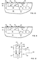
- Figs. 8 and 9 show still another variation of the invention.
- p-type body 80 has an epitaxial layer 83 formed thereon.
- this epitaxial layer there are two p+ regions, 81 and 82. Both of these regions 81 and 82 are generally rectangular in form, are hollow and concentric.
- the region 81 is buried at the juncture of the body 80 and the epitaxial layer 83 while the outer region 82 extends down from the surface of the epitaxial layer 83 to define an enclosed isolated region 85 of the epitaxial layer which also encloses the region 81.
- An oxide layer 86 overlies the entire epitaxial layer. Openings 87 and 88 are made in the oxide 86 and define a generally rectangular area of oxide 89.
- openings 87 and 88 each overlies approximately one-half of the p+ region 81. It should be noted that the openings 87 and 88 do not meet thus permitting the area 89 of oxide generally enclosed by the opening 87 and 88 to be connected to the main body by oxide bridges 90 and 91.
- a pit 79 is etched in the epitaxial layer 83 and body 80 beneath the oxide area 89. It should be noted that the pit exposes the p+ region 81.
- Metal electrodes 92 and 93 are deposited over the oxide area 89. It is to be noted that each electrode extends over a respective bridge 90 and 91 to respective metal lines 94 and 95 leading to respective epitaxial contacts 96 and 97 and off chip to a suitable biasing source.
- the device operates as follows. A voltage with respect to the substrate 80 is impressed on only one of the electrodes, say for example electrode 92.
- the electrostatic forces causes the oxide layer 89 over the pit 79 to rotate around the bridges 90 and 91 such that the electrode 92 goes towards the p+ region 81 and the'electrod.e 93 moves away from the p+ region 81.
- the enclosed epi pockets at each end are biased at the same potential as their corresponding electrodes thereby preventing lateral movement of the entire'beam.
- FIG. 10 illustrates in sectional form a transistor useful as an accelerometer.
- This comprises a p-type substrate 100, an n-type epitaxial layer 101 and n+ type diffusion 102 which can extend in part via reach through diffusion 102a to the surface of the epitaxial layer 101 and is contacted by a base electrode 103, a p-type region 104 contacted by electrode 105 serves as a collector and a second p-type region 106 contacted by electrode 107 serves as an emitter.
- the inertia of the aluminum slug 109 causes the beam to bend where it joins the emitter junction. This bending introduces stress into the junction and varies the emitter current at the biased voltage hence the collector voltage varies in accordance with the amount of acceleration.
- the feedback transistor is shown in Fig. 11.
- the transistor comprises a p-type substrate 112, an n-type epitaxial layer 113, an n+ type diffusion 114 which can extend in part to base contact 115, via reach thru diffusion 114a, a p-type collector 116 and contact 117, a p-type emitter 118 and contact 119 and an oxide beam 120 cantilevered over a pit 121 and p+ region 123.
- the beam 120 is coated with a metal electrode 122 so that the beam can be electrostatically bent to apply a predetermined stress on the emitter junction of the transistor.
- any acceleration experience by the device of Fig. 10 may be made proportional to the square of the voltage applied to beam electrode 122 located next to the emitter of the transistor of Figure 11.
- Figure 12 shows a suitable circuit and includes a transistor 125 formed as showing in Fig. 10 and a transistor 126 formed as shown in Fig. 11.
- a negative bias voltage source 127 is coupled through a resistor 128 to the collector of transistor 125 and through another resistor 130 to base of transistor 125 and thence through a third resistor 131 to the emitter of transistor 125 which is coupled to ground.
- the source 127 is coupled through a variable resistor 132 to the collector of the feedback transistor.
- An offset bias source 133 is coupled through a resistor 134 to base of transistor 126 and thence through a resistor 135 to the emitter of transistor 126 and ground.
- the collector voltage signals developed across resistors 128 and 132 are fed to differential amplifier 129.
- the output of the differential amplifier is connected to an out signal node 136 and to the beam electrode (i. e., electrode 122 op the beam 120) of the feedback transistor 126.
- the offset voltage on transistor 126 keeps the beam biased downwards and thus provides a fixed quiesent point for the circuit (to allow for + acceleration).
- a differential voltage occurs at the collectors of the two transistors. This voltage is related (in complex fashion) to the difference in stress encountered by transistor 125 due to the inertia of slug 109 and the stress encountered by transistor 126 due to the electrostatic forces on beam 120 produced by the voltage applied to electrode 122.
- the differential amplifier is connected in a feedback fashion such that it's output voltage, applied to electrode 122, causes the stress encountered by both transistors to equalize, thereby driving the differential collector voltages back to zero.
- the collector voltage on either transistor is a complex function of the stress applied to its associated beam, the fact that both transistors see equal stress, reduces the relation to a simple form. Since the stress on the accelerometer transistor is equal to a first constant times the acceleration and the stress on the feedback transistor is equal to a second constant times the square of the feedback voltage output of the differential amplifier applied to the beam electrode, it follows the acceleration is equal to a third constant times the square of the voltage applied to the feedback transistor beam.
Landscapes
- Engineering & Computer Science (AREA)
- Physics & Mathematics (AREA)
- General Physics & Mathematics (AREA)
- Theoretical Computer Science (AREA)
- Computer Hardware Design (AREA)
- Mechanical Light Control Or Optical Switches (AREA)
- Mechanical Optical Scanning Systems (AREA)
- Electrochromic Elements, Electrophoresis, Or Variable Reflection Or Absorption Elements (AREA)
- Semiconductor Integrated Circuits (AREA)
- Bipolar Transistors (AREA)
- Micromachines (AREA)
Applications Claiming Priority (2)
| Application Number | Priority Date | Filing Date | Title |
|---|---|---|---|
| US223522 | 1981-01-08 | ||
| US06/223,522 US4356730A (en) | 1981-01-08 | 1981-01-08 | Electrostatically deformographic switches |
Publications (2)
| Publication Number | Publication Date |
|---|---|
| EP0056084A1 true EP0056084A1 (de) | 1982-07-21 |
| EP0056084B1 EP0056084B1 (de) | 1985-05-29 |
Family
ID=22836876
Family Applications (1)
| Application Number | Title | Priority Date | Filing Date |
|---|---|---|---|
| EP81108117A Expired EP0056084B1 (de) | 1981-01-08 | 1981-10-09 | Elektrostatisch ablenkbare Schalter |
Country Status (5)
| Country | Link |
|---|---|
| US (1) | US4356730A (de) |
| EP (1) | EP0056084B1 (de) |
| JP (1) | JPS6014328B2 (de) |
| CA (1) | CA1163712A (de) |
| DE (1) | DE3170741D1 (de) |
Families Citing this family (59)
| Publication number | Priority date | Publication date | Assignee | Title |
|---|---|---|---|---|
| JP2631457B2 (ja) * | 1984-01-25 | 1997-07-16 | セイコーエプソン株式会社 | ライトバルブおよび投写型表示装置 |
| US4710732A (en) * | 1984-07-31 | 1987-12-01 | Texas Instruments Incorporated | Spatial light modulator and method |
| US4566935A (en) * | 1984-07-31 | 1986-01-28 | Texas Instruments Incorporated | Spatial light modulator and method |
| JPH0756531B2 (ja) * | 1984-07-31 | 1995-06-14 | テキサス インスツルメンツ インコーポレイテツド | 空間光変調器とその製法 |
| US4596992A (en) * | 1984-08-31 | 1986-06-24 | Texas Instruments Incorporated | Linear spatial light modulator and printer |
| ATE82076T1 (de) * | 1985-10-16 | 1992-11-15 | British Telecomm | Optische komponente mit wellenleiter. |
| US5172262A (en) * | 1985-10-30 | 1992-12-15 | Texas Instruments Incorporated | Spatial light modulator and method |
| CH670914A5 (de) * | 1986-09-10 | 1989-07-14 | Landis & Gyr Ag | |
| US4731670A (en) * | 1987-07-30 | 1988-03-15 | Eastman Kodak Company | Imaging apparatus |
| US4805038A (en) * | 1987-07-30 | 1989-02-14 | Eastman Kodak Company | Imaging apparatus which includes a light-valve array having electrostatically deflectable elements |
| US4956619A (en) * | 1988-02-19 | 1990-09-11 | Texas Instruments Incorporated | Spatial light modulator |
| DE68909075T2 (de) * | 1988-03-16 | 1994-04-07 | Texas Instruments Inc | Spatialer Lichtmodulator mit Anwendungsverfahren. |
| US4855544A (en) * | 1988-09-01 | 1989-08-08 | Honeywell Inc. | Multiple level miniature electromechanical accelerometer switch |
| US5966230A (en) * | 1990-05-29 | 1999-10-12 | Symbol Technologies, Inc. | Integrated scanner on a common substrate |
| US5625483A (en) * | 1990-05-29 | 1997-04-29 | Symbol Technologies, Inc. | Integrated light source and scanning element implemented on a semiconductor or electro-optical substrate |
| WO1992003740A1 (en) * | 1990-08-17 | 1992-03-05 | Analog Devices, Inc. | Monolithic accelerometer |
| US5314572A (en) * | 1990-08-17 | 1994-05-24 | Analog Devices, Inc. | Method for fabricating microstructures |
| US5326726A (en) * | 1990-08-17 | 1994-07-05 | Analog Devices, Inc. | Method for fabricating monolithic chip containing integrated circuitry and suspended microstructure |
| US5417111A (en) * | 1990-08-17 | 1995-05-23 | Analog Devices, Inc. | Monolithic chip containing integrated circuitry and suspended microstructure |
| US5212582A (en) * | 1992-03-04 | 1993-05-18 | Texas Instruments Incorporated | Electrostatically controlled beam steering device and method |
| FR2688315B1 (fr) * | 1992-03-09 | 1994-05-27 | Sagem | Capteur accelerometrique capacitif et accelerometre non asservi en comportant application. |
| US5307082A (en) * | 1992-10-28 | 1994-04-26 | North Carolina State University | Electrostatically shaped membranes |
| US5481396A (en) * | 1994-02-23 | 1996-01-02 | Aura Systems, Inc. | Thin film actuated mirror array |
| US5504504A (en) | 1994-07-13 | 1996-04-02 | Texas Instruments Incorporated | Method of reducing the visual impact of defects present in a spatial light modulator display |
| US5544268A (en) * | 1994-09-09 | 1996-08-06 | Deacon Research | Display panel with electrically-controlled waveguide-routing |
| US5630004A (en) * | 1994-09-09 | 1997-05-13 | Deacon Research | Controllable beam director using poled structure |
| US5552924A (en) | 1994-11-14 | 1996-09-03 | Texas Instruments Incorporated | Micromechanical device having an improved beam |
| US5579151A (en) * | 1995-02-17 | 1996-11-26 | Texas Instruments Incorporated | Spatial light modulator |
| US5696619A (en) * | 1995-02-27 | 1997-12-09 | Texas Instruments Incorporated | Micromechanical device having an improved beam |
| US5610438A (en) * | 1995-03-08 | 1997-03-11 | Texas Instruments Incorporated | Micro-mechanical device with non-evaporable getter |
| US6046840A (en) * | 1995-06-19 | 2000-04-04 | Reflectivity, Inc. | Double substrate reflective spatial light modulator with self-limiting micro-mechanical elements |
| US5771321A (en) * | 1996-01-04 | 1998-06-23 | Massachusetts Institute Of Technology | Micromechanical optical switch and flat panel display |
| US5638946A (en) * | 1996-01-11 | 1997-06-17 | Northeastern University | Micromechanical switch with insulated switch contact |
| US6054745A (en) * | 1999-01-04 | 2000-04-25 | International Business Machines Corporation | Nonvolatile memory cell using microelectromechanical device |
| JP4299407B2 (ja) * | 1999-08-30 | 2009-07-22 | ソニー株式会社 | メモリ装置 |
| FI109155B (fi) * | 2000-04-13 | 2002-05-31 | Nokia Corp | Menetelmä ja järjestely mikromekaanisen elementin ohjaamiseksi |
| US7099065B2 (en) * | 2000-08-03 | 2006-08-29 | Reflectivity, Inc. | Micromirrors with OFF-angle electrodes and stops |
| US7003187B2 (en) | 2000-08-07 | 2006-02-21 | Rosemount Inc. | Optical switch with moveable holographic optical element |
| US6810176B2 (en) | 2000-08-07 | 2004-10-26 | Rosemount Inc. | Integrated transparent substrate and diffractive optical element |
| US7196599B2 (en) * | 2000-12-11 | 2007-03-27 | Dabbaj Rad H | Electrostatic device |
| US6803534B1 (en) * | 2001-05-25 | 2004-10-12 | Raytheon Company | Membrane for micro-electro-mechanical switch, and methods of making and using it |
| JP2005519323A (ja) * | 2002-03-01 | 2005-06-30 | ローズマウント インコーポレイテッド | 三次元導光板を有する光学スイッチ |
| US7106066B2 (en) * | 2002-08-28 | 2006-09-12 | Teravicta Technologies, Inc. | Micro-electromechanical switch performance enhancement |
| US7405860B2 (en) * | 2002-11-26 | 2008-07-29 | Texas Instruments Incorporated | Spatial light modulators with light blocking/absorbing areas |
| US7274347B2 (en) * | 2003-06-27 | 2007-09-25 | Texas Instruments Incorporated | Prevention of charge accumulation in micromirror devices through bias inversion |
| US7787170B2 (en) * | 2004-06-15 | 2010-08-31 | Texas Instruments Incorporated | Micromirror array assembly with in-array pillars |
| US7113322B2 (en) * | 2004-06-23 | 2006-09-26 | Reflectivity, Inc | Micromirror having offset addressing electrode |
| US7092143B2 (en) * | 2004-10-19 | 2006-08-15 | Reflectivity, Inc | Micromirror array device and a method for making the same |
| US20060193028A1 (en) * | 2005-02-28 | 2006-08-31 | Satyadev Patel | Method of repairing micromirrors in spatial light modulators |
| US7375873B2 (en) * | 2005-02-28 | 2008-05-20 | Texas Instruments Incorporated | Method of repairing micromirrors in spatial light modulators |
| US7295363B2 (en) | 2005-04-08 | 2007-11-13 | Texas Instruments Incorporated | Optical coating on light transmissive substrates of micromirror devices |
| US7410901B2 (en) * | 2006-04-27 | 2008-08-12 | Honeywell International, Inc. | Submicron device fabrication |
| CN101617354A (zh) | 2006-12-12 | 2009-12-30 | 埃文斯和萨瑟兰计算机公司 | 用于校准单个调制器投影仪中的rgb光的系统和方法 |
| US8358317B2 (en) | 2008-05-23 | 2013-01-22 | Evans & Sutherland Computer Corporation | System and method for displaying a planar image on a curved surface |
| US8702248B1 (en) | 2008-06-11 | 2014-04-22 | Evans & Sutherland Computer Corporation | Projection method for reducing interpixel gaps on a viewing surface |
| US8077378B1 (en) | 2008-11-12 | 2011-12-13 | Evans & Sutherland Computer Corporation | Calibration system and method for light modulation device |
| US9641826B1 (en) | 2011-10-06 | 2017-05-02 | Evans & Sutherland Computer Corporation | System and method for displaying distant 3-D stereo on a dome surface |
| CN109879238A (zh) * | 2019-01-15 | 2019-06-14 | 江苏大学 | 内嵌通道式的微悬臂梁装置、加工方法及一种检测方法 |
| US11713240B2 (en) * | 2019-12-09 | 2023-08-01 | Board Of Regents, The University Of Texas System | Cellular array electrostatic actuator |
Citations (3)
| Publication number | Priority date | Publication date | Assignee | Title |
|---|---|---|---|---|
| EP0012243A1 (de) * | 1978-12-11 | 1980-06-25 | International Business Machines Corporation | Anzeigevorrichtung mit elektrostatisch ablenkbaren Elementen |
| GB1583536A (en) * | 1978-03-21 | 1981-01-28 | Singer Co | Electrostatic accelerometer |
| GB2075750A (en) * | 1980-05-08 | 1981-11-18 | Philips Nv | Programmable semiconductor devices |
Family Cites Families (8)
| Publication number | Priority date | Publication date | Assignee | Title |
|---|---|---|---|---|
| US3001447A (en) * | 1957-08-29 | 1961-09-26 | Zeiss Ikon A G Stuttgart | Image reproducing device for visible and invisible radiation images |
| US3081637A (en) * | 1960-02-17 | 1963-03-19 | Gen Precision Inc | Accelerometer and digital transmission means |
| US3137762A (en) * | 1960-06-30 | 1964-06-16 | Foerderung Forschung Gmbh | Arrangement for amplifying the brightness of an optically formed image |
| US3746911A (en) * | 1971-04-13 | 1973-07-17 | Westinghouse Electric Corp | Electrostatically deflectable light valves for projection displays |
| US3851522A (en) * | 1973-01-31 | 1974-12-03 | Westinghouse Electric Corp | Deceleration measuring apparatus |
| US3886310A (en) * | 1973-08-22 | 1975-05-27 | Westinghouse Electric Corp | Electrostatically deflectable light valve with improved diffraction properties |
| US3989890A (en) * | 1974-02-14 | 1976-11-02 | Westinghouse Electric Corporation | Optical imaging system utilizing a light valve array and a coupled photoemissive target |
| US4203128A (en) * | 1976-11-08 | 1980-05-13 | Wisconsin Alumni Research Foundation | Electrostatically deformable thin silicon membranes |
-
1981
- 1981-01-08 US US06/223,522 patent/US4356730A/en not_active Expired - Fee Related
- 1981-10-09 DE DE8181108117T patent/DE3170741D1/de not_active Expired
- 1981-10-09 EP EP81108117A patent/EP0056084B1/de not_active Expired
- 1981-11-20 JP JP56185624A patent/JPS6014328B2/ja not_active Expired
- 1981-12-11 CA CA000392092A patent/CA1163712A/en not_active Expired
Patent Citations (3)
| Publication number | Priority date | Publication date | Assignee | Title |
|---|---|---|---|---|
| GB1583536A (en) * | 1978-03-21 | 1981-01-28 | Singer Co | Electrostatic accelerometer |
| EP0012243A1 (de) * | 1978-12-11 | 1980-06-25 | International Business Machines Corporation | Anzeigevorrichtung mit elektrostatisch ablenkbaren Elementen |
| GB2075750A (en) * | 1980-05-08 | 1981-11-18 | Philips Nv | Programmable semiconductor devices |
Non-Patent Citations (3)
| Title |
|---|
| IBM Journal of Research and Development, Vol. 23, No. 4, July 1979 New York K.E. PETERSEN "Micromechanical Membrane Switches on Silicon", pages 376 to 385 * page 381, first and second paragraphs * * |
| IBM Technical Disclosure Bulletin, Vol. 21, No. 3, August 1978, New York K.E. PETERSEN et al. "Light-Activated Micromechanical Devices" pages 1205 to 1206 * |
| IEEE Transactions on Electron Devices, Vol. ED-26, No. 12, December 1979 New York L.M. ROYLANCE et al. "A Batch-Fabricated Silicon Accelerometer", pages 1911 to 1917 * setion II, pages 1911 to 1912 * * |
Also Published As
| Publication number | Publication date |
|---|---|
| JPS6014328B2 (ja) | 1985-04-12 |
| JPS57126164A (en) | 1982-08-05 |
| DE3170741D1 (en) | 1985-07-04 |
| EP0056084B1 (de) | 1985-05-29 |
| US4356730A (en) | 1982-11-02 |
| CA1163712A (en) | 1984-03-13 |
Similar Documents
| Publication | Publication Date | Title |
|---|---|---|
| US4356730A (en) | Electrostatically deformographic switches | |
| US4229732A (en) | Micromechanical display logic and array | |
| US4441791A (en) | Deformable mirror light modulator | |
| JP5475487B2 (ja) | マイクロメカニカル素子 | |
| JP2571877B2 (ja) | 非衝撃プリンタ | |
| CA1100614A (en) | Membrane deformographic display, and method of making | |
| US6495387B2 (en) | Electronic devices including micromechanical switches | |
| US4655554A (en) | Spatial light modulator having a capacitively coupled photoconductor | |
| US4672577A (en) | Three-dimensional integrated circuit with optically coupled shared memories | |
| US6137150A (en) | Semiconductor physical-quantity sensor having a locos oxide film, for sensing a physical quantity such as acceleration, yaw rate, or the like | |
| US4420897A (en) | Electroscopic display devices | |
| JPH06507718A (ja) | 集積化され整列されるトンネルチップペアを組み立てる方法 | |
| US4777516A (en) | Monolithic integration of light emitting elements and driver electronics | |
| EP0046873A1 (de) | Lichtmodulator mit verformbarem Spiegel | |
| US5172205A (en) | Piezoresistive semiconductor device suitable for use in a pressure sensor | |
| US5777352A (en) | Photodetector structure | |
| US6388252B1 (en) | Self-detecting type of SPM probe and SPM device | |
| KR100417481B1 (ko) | 메모리장치및그제조방법 | |
| SE461491B (sv) | Monolitisk optokopplare | |
| NL8901629A (nl) | Stralingsgevoelige halfgeleiderinrichting en uitlees- of schrijfeenheid bevattende een dergelijke stralingsgevoelige halfgeleiderinrichting. | |
| JPS6117151B2 (de) | ||
| US4679089A (en) | Solid state image sensor having an anti-blooming isolation electrode | |
| US4849805A (en) | Radiation hardened integrated circuit and method of making the same | |
| JPS6134263B2 (de) | ||
| JP3070118B2 (ja) | 半導体加速度センサ |
Legal Events
| Date | Code | Title | Description |
|---|---|---|---|
| PUAI | Public reference made under article 153(3) epc to a published international application that has entered the european phase |
Free format text: ORIGINAL CODE: 0009012 |
|
| 17P | Request for examination filed |
Effective date: 19811009 |
|
| AK | Designated contracting states |
Designated state(s): DE FR GB IT |
|
| GRAA | (expected) grant |
Free format text: ORIGINAL CODE: 0009210 |
|
| AK | Designated contracting states |
Designated state(s): DE FR GB IT |
|
| PG25 | Lapsed in a contracting state [announced via postgrant information from national office to epo] |
Ref country code: IT Free format text: LAPSE BECAUSE OF FAILURE TO SUBMIT A TRANSLATION OF THE DESCRIPTION OR TO PAY THE FEE WITHIN THE PRESCRIBED TIME-LIMIT;WARNING: LAPSES OF ITALIAN PATENTS WITH EFFECTIVE DATE BEFORE 2007 MAY HAVE OCCURRED AT ANY TIME BEFORE 2007. THE CORRECT EFFECTIVE DATE MAY BE DIFFERENT FROM THE ONE RECORDED. Effective date: 19850529 |
|
| REF | Corresponds to: |
Ref document number: 3170741 Country of ref document: DE Date of ref document: 19850704 |
|
| ET | Fr: translation filed | ||
| PLBE | No opposition filed within time limit |
Free format text: ORIGINAL CODE: 0009261 |
|
| STAA | Information on the status of an ep patent application or granted ep patent |
Free format text: STATUS: NO OPPOSITION FILED WITHIN TIME LIMIT |
|
| 26N | No opposition filed | ||
| PG25 | Lapsed in a contracting state [announced via postgrant information from national office to epo] |
Ref country code: GB Effective date: 19891009 |
|
| PGFP | Annual fee paid to national office [announced via postgrant information from national office to epo] |
Ref country code: DE Payment date: 19900307 Year of fee payment: 9 |
|
| GBPC | Gb: european patent ceased through non-payment of renewal fee | ||
| PG25 | Lapsed in a contracting state [announced via postgrant information from national office to epo] |
Ref country code: FR Effective date: 19900629 |
|
| REG | Reference to a national code |
Ref country code: FR Ref legal event code: ST |
|
| PG25 | Lapsed in a contracting state [announced via postgrant information from national office to epo] |
Ref country code: DE Effective date: 19910702 |