EP0055038A2 - Steuerung einer Signalspannung für eine Halbleitervorrichtung - Google Patents
Steuerung einer Signalspannung für eine Halbleitervorrichtung Download PDFInfo
- Publication number
- EP0055038A2 EP0055038A2 EP81305676A EP81305676A EP0055038A2 EP 0055038 A2 EP0055038 A2 EP 0055038A2 EP 81305676 A EP81305676 A EP 81305676A EP 81305676 A EP81305676 A EP 81305676A EP 0055038 A2 EP0055038 A2 EP 0055038A2
- Authority
- EP
- European Patent Office
- Prior art keywords
- voltage supply
- signal line
- semiconductor device
- layer
- level
- Prior art date
- Legal status (The legal status is an assumption and is not a legal conclusion. Google has not performed a legal analysis and makes no representation as to the accuracy of the status listed.)
- Granted
Links
Images

Classifications
-
- H—ELECTRICITY
- H10—SEMICONDUCTOR DEVICES; ELECTRIC SOLID-STATE DEVICES NOT OTHERWISE PROVIDED FOR
- H10W—GENERIC PACKAGES, INTERCONNECTIONS, CONNECTORS OR OTHER CONSTRUCTIONAL DETAILS OF DEVICES COVERED BY CLASS H10
- H10W42/00—Arrangements for protection of devices
-
- G—PHYSICS
- G11—INFORMATION STORAGE
- G11C—STATIC STORES
- G11C11/00—Digital stores characterised by the use of particular electric or magnetic storage elements; Storage elements therefor
- G11C11/21—Digital stores characterised by the use of particular electric or magnetic storage elements; Storage elements therefor using electric elements
- G11C11/34—Digital stores characterised by the use of particular electric or magnetic storage elements; Storage elements therefor using electric elements using semiconductor devices
- G11C11/40—Digital stores characterised by the use of particular electric or magnetic storage elements; Storage elements therefor using electric elements using semiconductor devices using transistors
- G11C11/401—Digital stores characterised by the use of particular electric or magnetic storage elements; Storage elements therefor using electric elements using semiconductor devices using transistors forming cells needing refreshing or charge regeneration, i.e. dynamic cells
- G11C11/4063—Auxiliary circuits, e.g. for addressing, decoding, driving, writing, sensing or timing
- G11C11/407—Auxiliary circuits, e.g. for addressing, decoding, driving, writing, sensing or timing for memory cells of the field-effect type
- G11C11/4074—Power supply or voltage generation circuits, e.g. bias voltage generators, substrate voltage generators, back-up power, power control circuits
-
- G—PHYSICS
- G11—INFORMATION STORAGE
- G11C—STATIC STORES
- G11C11/00—Digital stores characterised by the use of particular electric or magnetic storage elements; Storage elements therefor
- G11C11/21—Digital stores characterised by the use of particular electric or magnetic storage elements; Storage elements therefor using electric elements
- G11C11/34—Digital stores characterised by the use of particular electric or magnetic storage elements; Storage elements therefor using electric elements using semiconductor devices
- G11C11/40—Digital stores characterised by the use of particular electric or magnetic storage elements; Storage elements therefor using electric elements using semiconductor devices using transistors
- G11C11/401—Digital stores characterised by the use of particular electric or magnetic storage elements; Storage elements therefor using electric elements using semiconductor devices using transistors forming cells needing refreshing or charge regeneration, i.e. dynamic cells
- G11C11/4063—Auxiliary circuits, e.g. for addressing, decoding, driving, writing, sensing or timing
- G11C11/407—Auxiliary circuits, e.g. for addressing, decoding, driving, writing, sensing or timing for memory cells of the field-effect type
- G11C11/4076—Timing circuits
-
- G—PHYSICS
- G11—INFORMATION STORAGE
- G11C—STATIC STORES
- G11C11/00—Digital stores characterised by the use of particular electric or magnetic storage elements; Storage elements therefor
- G11C11/21—Digital stores characterised by the use of particular electric or magnetic storage elements; Storage elements therefor using electric elements
- G11C11/34—Digital stores characterised by the use of particular electric or magnetic storage elements; Storage elements therefor using electric elements using semiconductor devices
- G11C11/40—Digital stores characterised by the use of particular electric or magnetic storage elements; Storage elements therefor using electric elements using semiconductor devices using transistors
- G11C11/401—Digital stores characterised by the use of particular electric or magnetic storage elements; Storage elements therefor using electric elements using semiconductor devices using transistors forming cells needing refreshing or charge regeneration, i.e. dynamic cells
- G11C11/4063—Auxiliary circuits, e.g. for addressing, decoding, driving, writing, sensing or timing
- G11C11/407—Auxiliary circuits, e.g. for addressing, decoding, driving, writing, sensing or timing for memory cells of the field-effect type
- G11C11/409—Read-write [R-W] circuits
- G11C11/4094—Bit-line management or control circuits
-
- H—ELECTRICITY
- H10—SEMICONDUCTOR DEVICES; ELECTRIC SOLID-STATE DEVICES NOT OTHERWISE PROVIDED FOR
- H10D—INORGANIC ELECTRIC SEMICONDUCTOR DEVICES
- H10D84/00—Integrated devices formed in or on semiconductor substrates that comprise only semiconducting layers, e.g. on Si wafers or on GaAs-on-Si wafers
- H10D84/01—Manufacture or treatment
-
- H—ELECTRICITY
- H10—SEMICONDUCTOR DEVICES; ELECTRIC SOLID-STATE DEVICES NOT OTHERWISE PROVIDED FOR
- H10W—GENERIC PACKAGES, INTERCONNECTIONS, CONNECTORS OR OTHER CONSTRUCTIONAL DETAILS OF DEVICES COVERED BY CLASS H10
- H10W72/00—Interconnections or connectors in packages
Definitions
- This invention relates to a semiconductor device, and especially to a semiconductor device comprising a signal line in which a voltage higher than the supply voltage is generated.
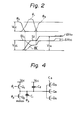
- FIG.l A known dynamic RAM semiconductor device in which a push-up circuit is used for the abovementioned purpose is illustrated in Fig.l of the accompanying drawings.
- This device has a push-up circuit PU, a precharger circuit PRE for a pair of bit lines BL and BL which are driven by the output of the push-up circuit PU, and a sense amplifier circuit SA for the memory cells.
- Fig.2 illustrates various voltage waveforms used to explain the operation of the push-up circuit PU of Fig.l.
- the push-up circuit PU consists of transistors Q 1 and Q 2 , a push-up capacitance C 1 and an output signal line S 1 , as illustrated in Fig.l.
- a clock signal ⁇ 1 is fed to the gate of the transistor Q 1 and another clock signal ⁇ 2 is fed to the gate of the transistor Q 2 .
- the clock ⁇ 1 is at first at an L (low) level and the clock ⁇ 2 is at the H(high) level so that the transistor Q 1 is OFF and the transistor Q 2 is ON; therefore, the level of the output signal line S 1 is kept at the L level (V SS ).
- the clock ⁇ 2 falls to the L level to turn off the transistor Q 2 ; after that, the clock ⁇ 1 rises to the H level (higher than V CC ) to fully turn on the transistor Q 1 so that the signal line S 1 is charged up to the V CC level. Under this condition, the clock ⁇ 1 falls to the L level to turn off the transistor Q 1 , and therefore the signal line S 1 is cut off from the voltage supply line Vcc . Then, the clock ⁇ 3 rises from the L level (V SS ) to the H level (V CC ) so that the level of the signal line S 1 is pushed up to a level V S1 higher than the voltage supply V CC through the capacity C 1 .
- the precharger circuit PRE consists of transistors Q 3 , Q 4 and Q 5 .
- the signal line S 1 is connected to all the gates of the transistors Q 3 , Q 4 and Q 5 .
- the drains of the transistors Q 3 and Q 4 are connected to the voltage supply V CC , and the sources of the transistors Q 3 and Q 4 are connected to the pair of bit lines BL and BL respectively.
- the drain and source of the transistor Q 5 are connected to the pair of bit lines BL and BL respectively.
- the sense amplifier circuit SA consists of transistors Q 6 , Q 7 and Q 8 as illustrated in Fig. 1.
- the drain of the transistor Q 6 and the gate of the transistor Q 7 are both connected to one line BL of the pair of bit lines, and the gate of the transistor Q6 and the drain of the transistor Q 7 are both connected to another line BL of the pair of bit lines.
- the sources of the transistors Q 6 and Q 7 are both connected to the drain of the transistor Q 8 , and the source of the transistor Q 8 is connected to the reference voltage V SS .
- the clock signal ⁇ 4 is applied to the gate of the transistor Q 8 .
- the sense amplifier circuit SA preceding the above-mentioned sense action, it is necessary to precharge the pair of bit lines BL and BL so as to make the potentials of the pair of bit lines BL and BL equal to each other.
- the clock ⁇ 1 rises to the H level as illustrated in Fig. 2
- the gate voltages of the transistors Q 3 Q 4 and Q 5 rise to the V CC level through the signal line S 1 and the pair of bit lines BL and BL are charged up from the voltage supply V CC through the transistors Q 3 and Q 4 , respectively.
- the transistor Q 5 is connected between the pair of bit lines BL and BL, and it becomes conductive in order to make the potentials of the pair of bit lines BL and BL equal to each other.
- the level of the signal line S 1 is nearly equal to the voltage supply V CC so that the transistors Q 3 , Q 4 and Q 5 are not turned on fully, and therefore the potentials of the pair of bit lines BL and BL are lower than V CC and are not completely equal to each other.
- the clock ⁇ 1 falls to the L level and the clock ⁇ 2 rises to the H level
- the level of the signal line S 1 rises from V CC to V S1 higher than V CC so that the transistors Q 3 , Q 4 and Q 5 are fully turned on and the pair of bit lines BL and BL are both charged up to the voltage supply level V CC .
- the level V S1 of the signal line S 1 is expressed by the following equation: In order to charge up the pair of bit lines BL and BL to the voltage supply level V CC , it is necessary that the second term of the right side of the equation (1) be greater than the threshold voltage V th of the transistors Q 3 , Q 4 and Q 5 .
- the voltage supply V CC may rise from 5 V to 5.5 V (V CC + ⁇ V CC ) after that.
- the value of "V CC " in the equation (1) will remain 5 V because at this time the clock ⁇ 1 has already fallen enough so that the transistor Q 1 is turned off.
- the response of the level of the signal line S 1 to the variance of the voltage supply V CC depends mainly on the dependence of the clock ⁇ 3 upon the voltage supply V CC .
- An increase in the level of the signal line S 1 is expressed by the following equation:
- the level of the signal line S 1 may increase only a little compared with the increase of V CC especially in the case that the capacity C 2 is relatively large (that is, the path of the signal line S 1 is long). Therefore, if the voltage supply V CC is changed, it may be that the level V S1 of the signal line S 1 can not be higher than the required level (V CC + V th ). In such a case, the short-circuit between the pair of bit lines BL and BL through the transistor 0 5 is insufficient so that the sense amplifier circuit SA may make an error.
- the potentials of the electrodes X opposite the signal line S 1 forming the capacity C 2 might be thought of as another factor in relation to the response of the level V S1 of the signal line S 1 .
- the signal line S 1 is formed to run the shortest path between the push-up circuit PU and the precharger circuit PRE, and therefore the opposite electrodes along the path of the signal line S 1 may be locally the ground line V SS , the semiconductor substrate itself, the other signal line, the node in the circuit or the voltage supply line V CC .
- the proportion of the path of the signal line S1 opposite the voltage supply V CC is generally small, and the potential of the opposite electrode X as a whole could be thought of as being other than the voltage supply V CC . Accordingly, in the semiconductor device of the prior art, improvement of the response of the level V S1 to V CC according to the opposite electrode X can not be expected.
- An object of the present invention is to alleviate the above-mentioned problem of the semiconductor device of the prior art, and to provide a semiconductor device which can operate stably,even when the voltage supply varies,by shielding the signal line generating a voltage higher than the voltage supply with the voltage supply line.
- a semiconductor device comprising a signal generating circuit in which an output of the circuit is cut off from a voltage supply line and an output signal higher than the voltage supply is generated at the output; a signal line layer connected to the output; and a transistor having a gate which is connected to the signal line layer and a drain which-is connected to the voltage supply line at least: a fter the output is cut off from the voltage supply line; characterised in that the semiconductor device also comprises means for following the voltage supply,which means causes the potential of the signal line layer to follow variations in potential of the voltage supply line after the signal line layer is cut off from the voltage supply line.
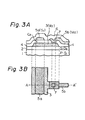
- FIG. 3A illustrates a principal sectional view of the above-mentioned semiconductor device
- Fig. 3B illustrates a plan pattern view of the device.
- the semiconductor device.of Figs. 3A and 3B comprises a p-type silicon semiconductor substrate 1, a silicon dioxide (Si0 2 ) layer 2 on the surface of the substrate 1, a polycrystal silicon layer 3 formed on the Si0 2 layer 2, a phosphosilicate glass (PSG) layer 4 for insulating between layers formed on the polycrystal silicon layer 3, aluminum (Al) wiring layers 5a and 5b upon the PSG layer 4, and a PSG layer 6 for covering the surface of the device.
- Si0 2 silicon dioxide
- PSG phosphosilicate glass
- the Al wiring layer 5b is a voltage supply (V CC ) line and is connected through the contact hole 7 to the polycrystal silicon layer 3 which is also used as a voltage supply line.
- the other Al wiring layer 5a is a signal line S 1 .
- the polycrystal silicon layer 3 is arranged to be laid under the Al wiring layer 5a through the insulating PSG layer 4 as much as possible. Though as a way to arrange the polycrystal silicon layer 3 as described above, it may be thought to crook the path of the Al wiring layer 5a, in accordance with the embodiment of Fig. 3A it is preferable that the Al wiring layer 5a remains as it is and the polycrystal silicon layer 3 is formed under the Al wiring layer 5a through the insulating PSG layer 4 even though the layer 3 is not necessary there.
- Fig. 4 illustrates an equivalent circuit diagram of the signal line S 1 of the semiconductor device of Fig. 3A.
- the potentials of the electrodes opposite the signal line S 1 are mainly the voltage supply V CC , and the portion of the signal line S 1 opposite the potentials other than the voltage supply V CC is considered to be negligibly small.
- the opposite potential of the capacity C 2 which is formed along the path of the signal line S1 is thought to be the voltage supply V CC as simplified.
- the level V S1 of the signal line S 1 is expressed by the above-mentioned equation (1). If, after the clock ⁇ 1 falls to the L level to cut off the signal line S 1 from the voltage supply line V CC , the voltage supply V CC rises by ⁇ V CC , the level V S1 of the signal line S 1 is pushed up not only by the clock ⁇ 3 through the capacity C 1 but also by the voltage supply itself through the capacity C 2 . Therefore, the level V S1 of the signal line S 1 would increase by ⁇ V S1 as expressed by the following equation:
- the level of the signal line S 1 can follow the variance of the voltage supply V CC even after the signal line S 1 is cut off from the voltage supply line V CC .
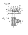
- a semiconductor in accordance with another embodiment of the present invention is illustrated in Figs. 5A and 5B.
- Fig. 5A illustrates a principal sectional view of the above-mentioned semiconductor device
- Fig. 5B illustrates a plan pattern view of the device.
- a N +- type diffusion layer 8 is formed upon a portion of the surface of the p-type silicon substrate 1
- a PSG layer 4 for insulating between layers is formed upon the field oxide (SiO 2 ) film 9 on the substrate 1 and upon the N +- type diffusion layer 8.
- Al wiring layers 5a and 5b for the signal line S 1 and for the voltage supply line V CC are formed on the insulating PSG layer 4.
- a covering PSG layer 6 is formed on the surface of the device.
- the Al wiring layer 5b is connected to the N + -type diffusion layer 8 through the contact hole 7. Therefore, a voltage supply wiring layer formed from the N +- type diffusion layer 8 is laid directly under the Al wiring layer 5a of the signal line S through the insulating PSG layer 4.
- the conductive layer laid under the signal line S 1 is formed as a voltage supply wiring line in the above-mentioned two embodiments
- the above--mentioned conductive layer may be formed as a signal line other than the voltage supply line which follows the variance of the voltage supply V CC .
- the present invention by means of extending the voltage supply line or another signal line equivalent to the voltage supply as much as possible under the output signal line of a push-up circuit or another circuit, the above-mentioned output signal line can be shielded equivalently, the level of the output signal line can follow variations in the voltage supply by the capacity formed along the output signal line, and the level of the output signal line can be made so as to be difficult to be influenced by the variance of the substrate potential.
Landscapes
- Engineering & Computer Science (AREA)
- Microelectronics & Electronic Packaging (AREA)
- Computer Hardware Design (AREA)
- Dram (AREA)
- Semiconductor Integrated Circuits (AREA)
- Design And Manufacture Of Integrated Circuits (AREA)
- Non-Volatile Memory (AREA)
Applications Claiming Priority (2)
| Application Number | Priority Date | Filing Date | Title |
|---|---|---|---|
| JP170748/80 | 1980-12-03 | ||
| JP55170748A JPS5846178B2 (ja) | 1980-12-03 | 1980-12-03 | 半導体装置 |
Publications (3)
| Publication Number | Publication Date |
|---|---|
| EP0055038A2 true EP0055038A2 (de) | 1982-06-30 |
| EP0055038A3 EP0055038A3 (en) | 1983-05-11 |
| EP0055038B1 EP0055038B1 (de) | 1986-08-06 |
Family
ID=15910651
Family Applications (1)
| Application Number | Title | Priority Date | Filing Date |
|---|---|---|---|
| EP81305676A Expired EP0055038B1 (de) | 1980-12-03 | 1981-12-02 | Steuerung einer Signalspannung für eine Halbleitervorrichtung |
Country Status (5)
| Country | Link |
|---|---|
| US (1) | US4482825A (de) |
| EP (1) | EP0055038B1 (de) |
| JP (1) | JPS5846178B2 (de) |
| DE (1) | DE3175075D1 (de) |
| IE (1) | IE52954B1 (de) |
Cited By (1)
| Publication number | Priority date | Publication date | Assignee | Title |
|---|---|---|---|---|
| DE3706251A1 (de) * | 1986-02-28 | 1987-09-03 | Canon Kk | Halbleitervorrichtung |
Families Citing this family (5)
| Publication number | Priority date | Publication date | Assignee | Title |
|---|---|---|---|---|
| JPS60201591A (ja) * | 1984-03-26 | 1985-10-12 | Hitachi Ltd | 半導体集積回路装置 |
| EP0481531B1 (de) * | 1987-05-21 | 1994-11-30 | Kabushiki Kaisha Toshiba | Ladungsübertragungsanordnung |
| JPH0192992A (ja) * | 1987-10-02 | 1989-04-12 | Matsushita Electric Ind Co Ltd | センスアンプ回路 |
| JP2621612B2 (ja) * | 1990-08-11 | 1997-06-18 | 日本電気株式会社 | 半導体集積回路 |
| US5258662A (en) * | 1992-04-06 | 1993-11-02 | Linear Technology Corp. | Micropower gate charge pump for power MOSFETS |
Family Cites Families (8)
| Publication number | Priority date | Publication date | Assignee | Title |
|---|---|---|---|---|
| US3646369A (en) * | 1970-08-28 | 1972-02-29 | North American Rockwell | Multiphase field effect transistor dc driver |
| JPS51111069A (en) * | 1975-03-26 | 1976-10-01 | Hitachi Ltd | Semiconductor device |
| JPS5279679A (en) * | 1975-12-26 | 1977-07-04 | Toshiba Corp | Semiconductor memory device |
| JPS5853512B2 (ja) * | 1976-02-13 | 1983-11-29 | 株式会社東芝 | 半導体記憶装置の製造方法 |
| DE2720533A1 (de) * | 1977-05-06 | 1978-11-09 | Siemens Ag | Monolithisch integrierte schaltungsanordnung mit ein-transistor- speicherelementen |
| US4250414A (en) * | 1978-07-31 | 1981-02-10 | Bell Telephone Laboratories, Incorporated | Voltage generator circuitry |
| US4369379A (en) * | 1980-03-14 | 1983-01-18 | Texas Instruments Incorporated | CMOS Frequency divider circuit having invalid signal override |
| US4398106A (en) * | 1980-12-19 | 1983-08-09 | International Business Machines Corporation | On-chip Delta-I noise clamping circuit |
-
1980
- 1980-12-03 JP JP55170748A patent/JPS5846178B2/ja not_active Expired
-
1981
- 1981-12-02 DE DE8181305676T patent/DE3175075D1/de not_active Expired
- 1981-12-02 EP EP81305676A patent/EP0055038B1/de not_active Expired
- 1981-12-02 US US06/326,899 patent/US4482825A/en not_active Expired - Lifetime
- 1981-12-03 IE IE2836/81A patent/IE52954B1/en not_active IP Right Cessation
Cited By (2)
| Publication number | Priority date | Publication date | Assignee | Title |
|---|---|---|---|---|
| DE3706251A1 (de) * | 1986-02-28 | 1987-09-03 | Canon Kk | Halbleitervorrichtung |
| US5150189A (en) * | 1986-02-28 | 1992-09-22 | Canon Kabushiki Kaisha | Semiconductor apparatus |
Also Published As
| Publication number | Publication date |
|---|---|
| EP0055038B1 (de) | 1986-08-06 |
| EP0055038A3 (en) | 1983-05-11 |
| IE52954B1 (en) | 1988-04-27 |
| JPS57103330A (en) | 1982-06-26 |
| JPS5846178B2 (ja) | 1983-10-14 |
| US4482825A (en) | 1984-11-13 |
| IE812836L (en) | 1982-06-03 |
| DE3175075D1 (en) | 1986-09-11 |
Similar Documents
| Publication | Publication Date | Title |
|---|---|---|
| KR0136560B1 (ko) | 반도체 기억장치 | |
| EP0046011B1 (de) | Halbleiterspeicheranordnung | |
| US7138684B2 (en) | Semiconductor memory device including an SOI substrate | |
| US5732014A (en) | Merged transistor structure for gain memory cell | |
| JP2918307B2 (ja) | 半導体記憶素子 | |
| US6381168B2 (en) | Circuits and methods for a memory cell with a trench plate trench capacitor and a vertical bipolar read device | |
| EP0087007B1 (de) | Dynamischer RAM Speicher mit einem nichtflüchtigen Hilfsspeicher und Betriebsverfahren dafür | |
| EP0135036A2 (de) | Halbleiterspeicher | |
| EP0055799A2 (de) | Nichtflüchtige dynamische RAM-Speicherzelle | |
| US4084108A (en) | Integrated circuit device | |
| US5051959A (en) | Complementary semiconductor memory device including cell access transistor and word line driving transistor having channels of different conductivity type | |
| US4156939A (en) | Integrated semiconductor memory device | |
| EP0167281A2 (de) | Halbleiterspeichergerät | |
| EP0163384B1 (de) | Leiteranordnung für die Energieversorgung in einer integrierten Schaltung | |
| KR930000759B1 (ko) | 다이나믹 메모리 | |
| EP0055038A2 (de) | Steuerung einer Signalspannung für eine Halbleitervorrichtung | |
| KR950008671B1 (ko) | 비트라인 사이에 감소된 기생용량을 갖는 반도체 기억장치 | |
| EP0037262B1 (de) | Halbleiterspeicheranordnung | |
| EP0037402B1 (de) | Halbleiterspeicher mit eine stabilisierten Substratspannung und einem Transfergate schmaler Breite | |
| JPS5948555B2 (ja) | ワンデバイス・メモリ・セル | |
| US5732037A (en) | Semiconductor memory | |
| EP0128273A2 (de) | Integrierter Halbleiterspeicher | |
| EP0212946A2 (de) | Halbleiterspeicheranordnung | |
| EP0089836A2 (de) | Statische Halbleiterspeicheranordnung | |
| US4492973A (en) | MOS Dynamic memory cells and method of fabricating the same |
Legal Events
| Date | Code | Title | Description |
|---|---|---|---|
| PUAI | Public reference made under article 153(3) epc to a published international application that has entered the european phase |
Free format text: ORIGINAL CODE: 0009012 |
|
| AK | Designated contracting states |
Designated state(s): DE FR GB NL |
|
| PUAL | Search report despatched |
Free format text: ORIGINAL CODE: 0009013 |
|
| AK | Designated contracting states |
Designated state(s): DE FR GB NL |
|
| 17P | Request for examination filed |
Effective date: 19831012 |
|
| GRAA | (expected) grant |
Free format text: ORIGINAL CODE: 0009210 |
|
| AK | Designated contracting states |
Kind code of ref document: B1 Designated state(s): DE FR GB NL |
|
| PG25 | Lapsed in a contracting state [announced via postgrant information from national office to epo] |
Ref country code: NL Effective date: 19860806 |
|
| ET | Fr: translation filed | ||
| REF | Corresponds to: |
Ref document number: 3175075 Country of ref document: DE Date of ref document: 19860911 |
|
| NLV1 | Nl: lapsed or annulled due to failure to fulfill the requirements of art. 29p and 29m of the patents act | ||
| PLBE | No opposition filed within time limit |
Free format text: ORIGINAL CODE: 0009261 |
|
| STAA | Information on the status of an ep patent application or granted ep patent |
Free format text: STATUS: NO OPPOSITION FILED WITHIN TIME LIMIT |
|
| 26N | No opposition filed | ||
| PGFP | Annual fee paid to national office [announced via postgrant information from national office to epo] |
Ref country code: GB Payment date: 19961125 Year of fee payment: 16 |
|
| PGFP | Annual fee paid to national office [announced via postgrant information from national office to epo] |
Ref country code: DE Payment date: 19961206 Year of fee payment: 16 |
|
| PGFP | Annual fee paid to national office [announced via postgrant information from national office to epo] |
Ref country code: FR Payment date: 19961211 Year of fee payment: 16 |
|
| PG25 | Lapsed in a contracting state [announced via postgrant information from national office to epo] |
Ref country code: GB Free format text: LAPSE BECAUSE OF NON-PAYMENT OF DUE FEES Effective date: 19971202 |
|
| PG25 | Lapsed in a contracting state [announced via postgrant information from national office to epo] |
Ref country code: FR Free format text: THE PATENT HAS BEEN ANNULLED BY A DECISION OF A NATIONAL AUTHORITY Effective date: 19971231 |
|
| GBPC | Gb: european patent ceased through non-payment of renewal fee |
Effective date: 19971202 |
|
| PG25 | Lapsed in a contracting state [announced via postgrant information from national office to epo] |
Ref country code: DE Free format text: LAPSE BECAUSE OF NON-PAYMENT OF DUE FEES Effective date: 19980901 |
|
| REG | Reference to a national code |
Ref country code: FR Ref legal event code: ST |