EP0053531A1 - Sammelschiene mit einem Stapel von 2N dielektrische Lagen in abwechselnder Anordnung mit 2N metallischen Lagen - Google Patents
Sammelschiene mit einem Stapel von 2N dielektrische Lagen in abwechselnder Anordnung mit 2N metallischen Lagen Download PDFInfo
- Publication number
- EP0053531A1 EP0053531A1 EP81401783A EP81401783A EP0053531A1 EP 0053531 A1 EP0053531 A1 EP 0053531A1 EP 81401783 A EP81401783 A EP 81401783A EP 81401783 A EP81401783 A EP 81401783A EP 0053531 A1 EP0053531 A1 EP 0053531A1
- Authority
- EP
- European Patent Office
- Prior art keywords
- bar according
- stack
- dielectric
- bars
- conductive
- Prior art date
- Legal status (The legal status is an assumption and is not a legal conclusion. Google has not performed a legal analysis and makes no representation as to the accuracy of the status listed.)
- Granted
Links
- 239000010408 film Substances 0.000 claims description 46
- 239000000853 adhesive Substances 0.000 claims description 29
- 230000001070 adhesive effect Effects 0.000 claims description 29
- 229910052751 metal Inorganic materials 0.000 claims description 18
- 239000002184 metal Substances 0.000 claims description 18
- 239000011104 metalized film Substances 0.000 claims description 9
- -1 polytetrafluoroethylene Polymers 0.000 claims description 6
- RYGMFSIKBFXOCR-UHFFFAOYSA-N Copper Chemical compound [Cu] RYGMFSIKBFXOCR-UHFFFAOYSA-N 0.000 claims description 5
- 229910052802 copper Inorganic materials 0.000 claims description 5
- 239000010949 copper Substances 0.000 claims description 5
- 229910052709 silver Inorganic materials 0.000 claims description 4
- 239000004332 silver Substances 0.000 claims description 4
- 229910052782 aluminium Inorganic materials 0.000 claims description 3
- XAGFODPZIPBFFR-UHFFFAOYSA-N aluminium Chemical compound [Al] XAGFODPZIPBFFR-UHFFFAOYSA-N 0.000 claims description 3
- 239000002033 PVDF binder Substances 0.000 claims description 2
- 239000004952 Polyamide Substances 0.000 claims description 2
- 239000004642 Polyimide Substances 0.000 claims description 2
- BQCADISMDOOEFD-UHFFFAOYSA-N Silver Chemical compound [Ag] BQCADISMDOOEFD-UHFFFAOYSA-N 0.000 claims description 2
- HCHKCACWOHOZIP-UHFFFAOYSA-N Zinc Chemical compound [Zn] HCHKCACWOHOZIP-UHFFFAOYSA-N 0.000 claims description 2
- PCHJSUWPFVWCPO-UHFFFAOYSA-N gold Chemical compound [Au] PCHJSUWPFVWCPO-UHFFFAOYSA-N 0.000 claims description 2
- 229910052737 gold Inorganic materials 0.000 claims description 2
- 239000010931 gold Substances 0.000 claims description 2
- 229920002492 poly(sulfone) Polymers 0.000 claims description 2
- 229920002647 polyamide Polymers 0.000 claims description 2
- 239000004417 polycarbonate Substances 0.000 claims description 2
- 229920000515 polycarbonate Polymers 0.000 claims description 2
- 229920000728 polyester Polymers 0.000 claims description 2
- 229920001721 polyimide Polymers 0.000 claims description 2
- 229920000098 polyolefin Polymers 0.000 claims description 2
- 229920001343 polytetrafluoroethylene Polymers 0.000 claims description 2
- 239000004810 polytetrafluoroethylene Substances 0.000 claims description 2
- 229920002981 polyvinylidene fluoride Polymers 0.000 claims description 2
- 229910052725 zinc Inorganic materials 0.000 claims description 2
- 239000011701 zinc Substances 0.000 claims description 2
- 239000010410 layer Substances 0.000 description 20
- 239000003292 glue Substances 0.000 description 6
- 238000000034 method Methods 0.000 description 5
- 239000012790 adhesive layer Substances 0.000 description 4
- 230000007547 defect Effects 0.000 description 4
- ATJFFYVFTNAWJD-UHFFFAOYSA-N Tin Chemical compound [Sn] ATJFFYVFTNAWJD-UHFFFAOYSA-N 0.000 description 3
- 230000005540 biological transmission Effects 0.000 description 3
- 229910010293 ceramic material Inorganic materials 0.000 description 3
- 239000004020 conductor Substances 0.000 description 3
- 238000005520 cutting process Methods 0.000 description 3
- 238000005259 measurement Methods 0.000 description 3
- 230000002787 reinforcement Effects 0.000 description 3
- 238000002048 anodisation reaction Methods 0.000 description 2
- 239000003989 dielectric material Substances 0.000 description 2
- 229920006332 epoxy adhesive Polymers 0.000 description 2
- 239000003302 ferromagnetic material Substances 0.000 description 2
- 238000009413 insulation Methods 0.000 description 2
- 238000004519 manufacturing process Methods 0.000 description 2
- 239000000463 material Substances 0.000 description 2
- 229920000139 polyethylene terephthalate Polymers 0.000 description 2
- 239000005020 polyethylene terephthalate Substances 0.000 description 2
- 229920002635 polyurethane Polymers 0.000 description 2
- 239000004814 polyurethane Substances 0.000 description 2
- 239000000843 powder Substances 0.000 description 2
- 229920005989 resin Polymers 0.000 description 2
- 239000011347 resin Substances 0.000 description 2
- 238000007650 screen-printing Methods 0.000 description 2
- 238000005507 spraying Methods 0.000 description 2
- 239000002966 varnish Substances 0.000 description 2
- 101100161175 Caenorhabditis elegans sur-6 gene Proteins 0.000 description 1
- 239000004593 Epoxy Substances 0.000 description 1
- 239000004677 Nylon Substances 0.000 description 1
- 229920002292 Nylon 6 Polymers 0.000 description 1
- 239000004962 Polyamide-imide Substances 0.000 description 1
- 239000004698 Polyethylene Substances 0.000 description 1
- 239000004743 Polypropylene Substances 0.000 description 1
- 239000004793 Polystyrene Substances 0.000 description 1
- 241001080024 Telles Species 0.000 description 1
- 239000002390 adhesive tape Substances 0.000 description 1
- 230000000712 assembly Effects 0.000 description 1
- 238000000429 assembly Methods 0.000 description 1
- 239000000919 ceramic Substances 0.000 description 1
- 238000001816 cooling Methods 0.000 description 1
- 230000006378 damage Effects 0.000 description 1
- 230000007423 decrease Effects 0.000 description 1
- 230000006866 deterioration Effects 0.000 description 1
- 238000010790 dilution Methods 0.000 description 1
- 239000012895 dilution Substances 0.000 description 1
- 238000009826 distribution Methods 0.000 description 1
- 230000009977 dual effect Effects 0.000 description 1
- 239000012948 isocyanate Substances 0.000 description 1
- 150000002513 isocyanates Chemical class 0.000 description 1
- 239000000203 mixture Substances 0.000 description 1
- 229920001778 nylon Polymers 0.000 description 1
- 239000003973 paint Substances 0.000 description 1
- 239000008188 pellet Substances 0.000 description 1
- 229920002312 polyamide-imide Polymers 0.000 description 1
- 229920000573 polyethylene Polymers 0.000 description 1
- 239000004848 polyfunctional curative Substances 0.000 description 1
- 229920001155 polypropylene Polymers 0.000 description 1
- 229920002223 polystyrene Polymers 0.000 description 1
- 238000000926 separation method Methods 0.000 description 1
- 239000002356 single layer Substances 0.000 description 1
- 239000007787 solid Substances 0.000 description 1
- 239000000243 solution Substances 0.000 description 1
- 239000002904 solvent Substances 0.000 description 1
- 229920001169 thermoplastic Polymers 0.000 description 1
- 239000004416 thermosoftening plastic Substances 0.000 description 1
- 235000012431 wafers Nutrition 0.000 description 1
Images
Classifications
-
- H—ELECTRICITY
- H05—ELECTRIC TECHNIQUES NOT OTHERWISE PROVIDED FOR
- H05K—PRINTED CIRCUITS; CASINGS OR CONSTRUCTIONAL DETAILS OF ELECTRIC APPARATUS; MANUFACTURE OF ASSEMBLAGES OF ELECTRICAL COMPONENTS
- H05K1/00—Printed circuits
- H05K1/02—Details
- H05K1/0213—Electrical arrangements not otherwise provided for
- H05K1/0263—High current adaptations, e.g. printed high current conductors or using auxiliary non-printed means; Fine and coarse circuit patterns on one circuit board
-
- H—ELECTRICITY
- H01—ELECTRIC ELEMENTS
- H01P—WAVEGUIDES; RESONATORS, LINES, OR OTHER DEVICES OF THE WAVEGUIDE TYPE
- H01P3/00—Waveguides; Transmission lines of the waveguide type
- H01P3/02—Waveguides; Transmission lines of the waveguide type with two longitudinal conductors
- H01P3/08—Microstrips; Strip lines
-
- H—ELECTRICITY
- H02—GENERATION; CONVERSION OR DISTRIBUTION OF ELECTRIC POWER
- H02G—INSTALLATION OF ELECTRIC CABLES OR LINES, OR OF COMBINED OPTICAL AND ELECTRIC CABLES OR LINES
- H02G5/00—Installations of bus-bars
- H02G5/005—Laminated bus-bars
-
- H—ELECTRICITY
- H05—ELECTRIC TECHNIQUES NOT OTHERWISE PROVIDED FOR
- H05K—PRINTED CIRCUITS; CASINGS OR CONSTRUCTIONAL DETAILS OF ELECTRIC APPARATUS; MANUFACTURE OF ASSEMBLAGES OF ELECTRICAL COMPONENTS
- H05K2201/00—Indexing scheme relating to printed circuits covered by H05K1/00
- H05K2201/10—Details of components or other objects attached to or integrated in a printed circuit board
- H05K2201/10227—Other objects, e.g. metallic pieces
- H05K2201/10272—Busbars, i.e. thick metal bars mounted on the printed circuit board [PCB] as high-current conductors
-
- H—ELECTRICITY
- H05—ELECTRIC TECHNIQUES NOT OTHERWISE PROVIDED FOR
- H05K—PRINTED CIRCUITS; CASINGS OR CONSTRUCTIONAL DETAILS OF ELECTRIC APPARATUS; MANUFACTURE OF ASSEMBLAGES OF ELECTRICAL COMPONENTS
- H05K2201/00—Indexing scheme relating to printed circuits covered by H05K1/00
- H05K2201/10—Details of components or other objects attached to or integrated in a printed circuit board
- H05K2201/10431—Details of mounted components
- H05K2201/10507—Involving several components
- H05K2201/10515—Stacked components
-
- H—ELECTRICITY
- H05—ELECTRIC TECHNIQUES NOT OTHERWISE PROVIDED FOR
- H05K—PRINTED CIRCUITS; CASINGS OR CONSTRUCTIONAL DETAILS OF ELECTRIC APPARATUS; MANUFACTURE OF ASSEMBLAGES OF ELECTRICAL COMPONENTS
- H05K2201/00—Indexing scheme relating to printed circuits covered by H05K1/00
- H05K2201/10—Details of components or other objects attached to or integrated in a printed circuit board
- H05K2201/10613—Details of electrical connections of non-printed components, e.g. special leads
- H05K2201/10621—Components characterised by their electrical contacts
- H05K2201/10689—Leaded Integrated Circuit [IC] package, e.g. dual-in-line [DIL]
Definitions
- the present invention relates to power bars of characteristic low impedance for the transmission of an electrical signal from a source to a plurality of receivers, said power bar comprising in particular two conductive bars carrying the current separated by dielectric means.
- bus-bar Such power bars, also known by the Anglo-Saxon name “bus-bar”, have been used for a very long time in particular in power systems for computer electrical circuits.
- the power bar When it is desired to supply, for example, a few integrated circuits arranged on a printed circuit, the power bar must of course not have an excessive width compared to the width of the boxes of said integrated circuits. However, if it is desired to produce supply bars having a very high capacity, it is possible either to produce large width bars with a single layer of very thin dielectric film interposed between the supply bars, or to produce a supply bar as described in US Patent 3,312,870.
- said feed bars are too bulky and too fragile.
- the conductive bars generally metallic, have a fairly approximate surface state, that is to say that there are metallic protrusions a few microns thick in places.
- the power bars thus produced are too thick to be used in certain applications, especially when it is desired to place said bars under the housings of integrated circuits of the DIL type, between the "tabs" of said integrated circuits. .
- the power bars according to the invention do not have the drawbacks of the power bars described above and respond to the problem posed.
- the supply bars according to the invention are characterized in that said dielectric means consist of a stack of metallized dielectric films forming a set of 2 n dielectric films, identical or different, separated by 2 n metallic layers, the metallic layers of even and odd rows being respectively connected to each other laterally by electrical connections, the conductive bars being fixed on either side of the stack and connected electrically, respectively to one of the lateral electrical connections.
- Metallized films can be covered with metal on one or both sides. In the latter case, there will be found in the stack of metal layers formed by two superimposed layers which will therefore be electrically connected to each other by contact.
- cushioning means will be interposed between the stack and each of the conductive bars, the aim of which is above all to prevent deterioration of the layers of the stack.
- the thickness of said cushions will be greater than or equal to 10 microns.
- These cushions may consist of either an adhesive such as an epoxy adhesive, an isocyanate, a polyurethane or a mixture of these with their respective hardeners (mono or two-component adhesives), this adhesive being insulating to the conductor, or an electrically inactive layer formed of a flexible dielectric film.
- the cushion-forming means can fulfill the dual function on the one hand of allowing assembly between the stack of dielectric films and the conductive bars, and on the other hand of avoiding direct contact between the metallized films and said conductive bars, in order to avoid mechanical injuries from each other.
- an adhesive will preferably be used which, depending on the case, for example the shape of the supply bar produced, will be insulating or conductive.
- conductive adhesive either conductive varnishes or conductive glues can be used.
- the conductive nature of these varnishes or glues is generally given by the presence of a metal powder in fairly large quantity therein.
- the metal powder is silver, known for its very good conductive properties.
- insulating adhesives all types of adhesives well known to those skilled in the art, one or two-component may be used.
- adhesives of the polyurethane and / or epoxy type may be used.
- the cushion-forming means consist of an electrically inactive layer, formed of a flexible dielectric film
- this may be identical to or different from one of the dielectrics of the stack. It will preferably be chosen from the same family, described below.
- This film will be made integral with the stack either using an adhesive or using the lateral electrical connections: these are generally obtained by spraying molten metal, the dielectric film is thus included in the stacked by projected metal.
- This film will be made integral with the conductive bars, generally using an adhesive as defined above.
- the feed bar according to the invention it is possible to introduce into the stack m layers of adhesive, arranged between the 2 n layers of metallized films, m being less than or equal to 2 n - 1. Depending on the desired result, we can vary m from 1 to 2 n -1.
- the thickness of the adhesive preferably chosen from common commercially available adhesives, as described above, will generally vary between 0.2 and 2 microns.
- Such power bars have significant advantages over known power bars, including those having two conductive bars separated by an adhesive dielectric film.
- the power bars according to the invention have the property of being self-healing.
- the phenomenon of self-healing is as follows: when the dielectric film has defects also called "conductive points", the tensioning of the conductive bar, that is to say the appearance of a potential difference between the two conductive bars, causes the volatilization of the parts of metallic reinforcement opposite the conductive point, without perforation of the dielectric. In this way, the power bar can still be used, no short-circuit appearing between the busbars.
- the metallized films used to make the bars according to the invention allowing said bar to undergo a high voltage gradient, the dielectric used can have a low thickness, which results in a significant increase in capacity. ie the power bar according to the invention has a very low characteristic impedance. In the context of the invention, it is indeed possible to use dielectric films with a thickness of the order of 1.5 microns while having an operating voltage greater than 100 volts.
- the dielectric film in the case of solid reinforcements, must have a thickness of at least 20 microns so that the supply bar has a correct reliability of use. Under these conditions, the capacity per unit length of said bar is obviously much lower, which results in a much higher characteristic impedance and a power bar ill-suited to the problem to be solved.
- the characteristic impedance of the bars according to the invention remains low even at very high frequencies, unlike those using a ceramic material with a high dielectric constant. Indeed, in the case of ceramic material, the dielectric losses at high frequency introduce a series resistance in the circuit which degrades the characteristic impedance of the lines thus produced.
- the supply bars according to the invention can be cut to the desired length without any risk of short circuit between the conductive bars. Indeed, the presence of the cushions allows sufficient separation of the bars from one another.
- the power bars according to the invention can be used, as will be described later, either vertically, that is to say arranged between the integrated circuits of the printed circuit board, or horizontally, that is to say - say under the integrated circuits between their connection lugs.
- the conductive bars When these power bars are used vertically, the conductive bars have their connections intended to be fixed in the holes of the printed circuits, located on the same side of a lateral electrical connection.
- said conductive bars will therefore be fixed on either side of the stack of metallized dielectric films using two different adhesives, the part of the conductive bar located near the lateral electrical connection to which it must be connected being fixed with an electrically conductive adhesive, while the other part of the conductive bar located opposite the electrical connection to ' , which it must not be connected will be fixed to the using an electrically non-conductive adhesive or film.
- any dielectric film having suitable properties well known to those skilled in the art may be used.
- common dielectric films such as paper, polyolefins and in particular polypropylene and polyethylene, polycarbonate, polysulfone, polystyrene, or polyesters such as polyethylene terephthalate will be used, these being generally the films preferred in the context of the present invention (in particular because of their high dielectric constant).
- other dielectric films such as polyamide films (nylon 6, nylon 6.6, etc.), polyimide, polyamide-imide, polytetrafluoroethylene, polyvinylidene fluoride, etc.
- the thickness of the film used will be as small as possible, since the capacity of the bar increases when the thickness of the dielectric decreases. This will generally be less than 20 microns, and preferably less than 5 microns.
- the type of dielectric, its thickness, etc. will be chosen so that a capacity per centimeter of length of power bars greater than 20 nanofarads is obtained. It is in fact considered that this value is a minimum value in order to obtain power bars with a low distributed constant enabling all the signals to be transmitted, from continuous to several hundred MHz. This is what makes the production of these power bars particularly delicate.
- the metal which can be used to metallize the surface of the dielectric film will preferably be zinc, aluminum, silver, gold or copper.
- the thickness of the metallic layer deposited on the dielectric film will be such that the "square" resistance of the metallized film varies between 0.5 ohm and 5 ohms.
- square resistance is meant the resistance of the metallic layer of a square of metallized film of, for example, a centimeter of side.
- the conductive bars will generally be made of very conductive material, such as copper.
- this conductive material will be covered with a layer of tin, deposited before or after cutting of said bars.
- This tinning will be carried out, in a manner known per se, either chemically or electrolytically.
- the thickness of the tin layer will preferably be 20 microns.
- power bars will generally be produced comprising between four and twenty layers of metallized dielectric film, the other elements of the bar being chosen so that the total thickness thereof remains less than 3 mm. These data correspond to the best embodiment of the invention.
- the stacking of the metallized dielectric films is first carried out and their assembly by lateral projection of metal.
- This technique is in itself well known and described for example in French patent N ° 903,040.
- the stacks thus produced are then cut to the desired length and assembled with the conduc bars. corresponding trices.
- These can be in the form of rolls which are unrolled during assembly with the dielectric stacks, each bar being previously coated with a layer of glue at the desired locations, for example using a drum. provided with a silk screen which allows the continuous deposit of the glue by screen printing.
- the viscosity of the adhesives used will be adjusted by more or less dilution in an appropriate solvent.
- This protection can also be a paint, a thermo-plastic or adhesive tape, etc.
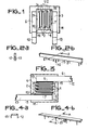
- the dielectric films 1 respectively covered with metallic layers 2 are offset with respect to each other, the layers of the same rank (even and odd) being connected between them by lateral electrical connections such as 3 and 4.
- the conductive bars 5 and 6 are assembled on either side of the stack of metallized dielectric films using insulating adhesive layers such as 7 and 9, and of conductive adhesive layers such as 8 and 10. It is noted in this figure, that, to ensure better electrical contact between the lateral electrical connections 3 and 4 and the adhesive layers 8 and 10, these terminate in menisci 14 and 15 which correspond to the filling of the re-entrant dihedrons formed by the lateral electrical connections 3 and 4 and the supply bars 5 and 6.
- FIG. 2 a feed bar is shown substantially on scale 1.
- this bar is viewed from the front with its sets of connection lugs 12 and 13, while FIG. 2 b represents a section along AA in Figure 2 a-
- the configuration of the bar shown in Figures 1 and 2 corresponds to the so-called "vertical" configuration of said bar.
- FIG. 3 a second alternative embodiment of the power bars according to the invention is shown, corresponding to the so-called "horizontal" configuration.
- the same elements as those of the previous figures have the same references.
- the only difference in this FIG. 3 is constituted by the arrangement of the conductive bars 5 and 6.
- These conductive bars have their respective connection tabs 12 and 13 situated on the same side as the lateral electrical connections 3 and 4 to which they are respectively connected.
- the upper parts 16 and 17 conductive bars are located approximately the same height as the wafers of metallized dielectric films to which they are connected.
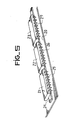
- FIG. 4a there is shown a view on scale approximately 1a of a feed bar as described in FIG. 3.
- This feed bar is of very flat shape, which makes it possible to use it in particular as shown in FIG. 5 for supplying integrated circuits such as 21, 22, 23 arranged on a printed board 20.
- the power bar 24 conforms to that described in FIGS. 3 and 4, can be housed between the connection tabs such as 25, 26 and 27 of said integrated circuits.
- connection tabs such as 25, 26 and 27 of said integrated circuits.
- EXAMPLE A polyethylene terephthalate film, with a dielectric constant of 3.2, is coated with a layer of vacuum-deposited aluminum of thickness substantially equal to 200 Angstroems, representing a square resistance of approximately 1.5 ohm . This film is cut into strips approximately 5 mm wide. On each of these strips, a small margin was made by removing the metal layer on one of the sides. The metallized films are then stacked according to the technique described in French patent 903,040, then the lateral electrical connections are made by spraying metal. After cooling, the stacks thus produced are cut into pieces of approximately 20 cm in length. Two metallic copper bars having lateral connection tabs regularly spaced along their length, and previously tinned, are then assembled with the stack produced above. To achieve this assembly, the metal bars are screen-printed with a single-component conductive epoxy adhesive containing 60% pure silver. After the glue has dried and polymerized, the feed bar is then subjected to the marking operation and is ready for use.
- the measurement of the resistance per unit length of the power bar according to the invention is for the 6 samples previously used between 0.21 and 0.22 milliohm per centimeter. Since the copper used has a resistivity of 0.017 ohm x square millimeter per millimeter, the theoretical resistance of these bars is equal to 0.21 milliohm per centimeter. It is therefore quite remarkable that the power bars according to the invention do not cause disturbances in the value of the resistance of the conductive bars used.
- the characteristic impedance of the bars measured using a pulse generator with a rise time of less than 5 nanoseconds made it possible to find an average characteristic impedance on the 6 samples mentioned above equal to 0, 31 ohm, the corresponding theoretical calculated value being 0.22 ohm.
- power bar (or “bus-bar” according to the English name) has generally been used. Saxon). It is obvious that this term in no way limits the function of these bars to a means of connection of a supply voltage source to a plurality of circuits. On the contrary, it designates a means of connecting any generator (source) of a continuous or alternating electrical signal, analog or digital to any receiver using this signal.
Landscapes
- Engineering & Computer Science (AREA)
- Microelectronics & Electronic Packaging (AREA)
- Fixed Capacitors And Capacitor Manufacturing Machines (AREA)
- Structure Of Printed Boards (AREA)
- Insulated Conductors (AREA)
Applications Claiming Priority (2)
| Application Number | Priority Date | Filing Date | Title |
|---|---|---|---|
| FR8025270 | 1980-11-28 | ||
| FR8025270A FR2495387A1 (fr) | 1980-11-28 | 1980-11-28 | Barre d'alimentation comportant un empilement de 2 n couches metalliques separees par 2 n couches dielectriques |
Publications (2)
| Publication Number | Publication Date |
|---|---|
| EP0053531A1 true EP0053531A1 (de) | 1982-06-09 |
| EP0053531B1 EP0053531B1 (de) | 1984-08-22 |
Family
ID=9248444
Family Applications (1)
| Application Number | Title | Priority Date | Filing Date |
|---|---|---|---|
| EP81401783A Expired EP0053531B1 (de) | 1980-11-28 | 1981-11-10 | Sammelschiene mit einem Stapel von 2N dielektrische Lagen in abwechselnder Anordnung mit 2N metallischen Lagen |
Country Status (5)
| Country | Link |
|---|---|
| US (1) | US4401844A (de) |
| EP (1) | EP0053531B1 (de) |
| BR (1) | BR8107696A (de) |
| DE (1) | DE3165709D1 (de) |
| FR (1) | FR2495387A1 (de) |
Cited By (1)
| Publication number | Priority date | Publication date | Assignee | Title |
|---|---|---|---|---|
| FR2530086A1 (fr) * | 1982-07-09 | 1984-01-13 | Europ Composants Electron | Procede de raccordement electrique d'une barre d'interconnexion |
Families Citing this family (17)
| Publication number | Priority date | Publication date | Assignee | Title |
|---|---|---|---|---|
| US4494170A (en) * | 1983-11-14 | 1985-01-15 | Rogers Corporation | Decoupling capacitor and method of manufacture thereof |
| US4532572A (en) * | 1983-11-14 | 1985-07-30 | Rogers Corporation | Decoupling capacitor and method of manufacture thereof |
| US4536826A (en) * | 1984-09-10 | 1985-08-20 | At&T Bell Laboratories | Snap-in bus bar |
| AU574908B2 (en) * | 1985-02-13 | 1988-07-14 | Fujitsu Limited | Electronic apparatus mounting structure |
| US5166867A (en) * | 1985-12-31 | 1992-11-24 | Fujitsu Limited | Bus bar for a circuit board |
| DE4031203A1 (de) * | 1990-10-04 | 1992-04-09 | Bosch Gmbh Robert | Dickschichthybridanordnung mit aussenkontakten |
| US5306874A (en) * | 1991-07-12 | 1994-04-26 | W.I.T. Inc. | Electrical interconnect and method of its manufacture |
| DE19507790C1 (de) * | 1995-03-06 | 1996-03-21 | Siemens Nixdorf Inf Syst | Stromschienen mit Siebkondensatoren |
| US5875091A (en) * | 1997-01-07 | 1999-02-23 | Siemens Nixdorf Informationssysteme Aktiengesellschaft | Busbars with filter capacitors |
| US6916990B2 (en) * | 2002-09-30 | 2005-07-12 | Teradyne, Inc. | High power interface |
| US20040154829A1 (en) * | 2003-01-31 | 2004-08-12 | Sass Forrest L. | Low inductance high capacitance power cable for connecting a power supply to an electrical load |
| JP4314513B2 (ja) * | 2003-06-18 | 2009-08-19 | アイシン・エィ・ダブリュ株式会社 | インバータノイズ除去装置 |
| US20050109856A1 (en) * | 2003-11-25 | 2005-05-26 | Alexander James N.Iv | Method for preparing polymer electrosprays |
| JP4952123B2 (ja) * | 2005-12-13 | 2012-06-13 | パナソニック株式会社 | コンデンサユニット |
| US8643380B1 (en) * | 2010-07-15 | 2014-02-04 | Edward Herbert | Method and apparatus for reducing shock and arc-flash hazards in power distribution systems |
| DE102012222423B4 (de) * | 2012-12-06 | 2021-05-20 | Siemens Aktiengesellschaft | Vorrichtung zur Isolation von Leitern |
| US20240429686A1 (en) * | 2023-06-20 | 2024-12-26 | Abb Schweiz Ag | Electrical busway assemblies and methods of assembling same |
Citations (2)
| Publication number | Priority date | Publication date | Assignee | Title |
|---|---|---|---|---|
| US3312870A (en) * | 1964-03-13 | 1967-04-04 | Hughes Aircraft Co | Electrical transmission system |
| US3520987A (en) * | 1968-08-05 | 1970-07-21 | Eldre Components | High capacity bus bar |
Family Cites Families (4)
| Publication number | Priority date | Publication date | Assignee | Title |
|---|---|---|---|---|
| US3189847A (en) * | 1961-05-29 | 1965-06-15 | Ibm | D. c. power distribution system |
| US3351876A (en) * | 1964-10-26 | 1967-11-07 | Hughes Aircraft Co | Electrical transmission system |
| FR2138403B1 (de) * | 1971-05-25 | 1976-12-03 | Europ Composants Electron | |
| US4236046A (en) * | 1978-10-10 | 1980-11-25 | Rogers Corporation | High capacitance bus bar |
-
1980
- 1980-11-28 FR FR8025270A patent/FR2495387A1/fr active Granted
-
1981
- 1981-11-10 DE DE8181401783T patent/DE3165709D1/de not_active Expired
- 1981-11-10 EP EP81401783A patent/EP0053531B1/de not_active Expired
- 1981-11-24 US US06/324,608 patent/US4401844A/en not_active Expired - Fee Related
- 1981-11-28 BR BR8107696A patent/BR8107696A/pt unknown
Patent Citations (2)
| Publication number | Priority date | Publication date | Assignee | Title |
|---|---|---|---|---|
| US3312870A (en) * | 1964-03-13 | 1967-04-04 | Hughes Aircraft Co | Electrical transmission system |
| US3520987A (en) * | 1968-08-05 | 1970-07-21 | Eldre Components | High capacity bus bar |
Cited By (1)
| Publication number | Priority date | Publication date | Assignee | Title |
|---|---|---|---|---|
| FR2530086A1 (fr) * | 1982-07-09 | 1984-01-13 | Europ Composants Electron | Procede de raccordement electrique d'une barre d'interconnexion |
Also Published As
| Publication number | Publication date |
|---|---|
| BR8107696A (pt) | 1982-08-24 |
| EP0053531B1 (de) | 1984-08-22 |
| FR2495387B1 (de) | 1983-11-25 |
| DE3165709D1 (en) | 1984-09-27 |
| US4401844A (en) | 1983-08-30 |
| FR2495387A1 (fr) | 1982-06-04 |
Similar Documents
| Publication | Publication Date | Title |
|---|---|---|
| EP0053531B1 (de) | Sammelschiene mit einem Stapel von 2N dielektrische Lagen in abwechselnder Anordnung mit 2N metallischen Lagen | |
| EP0086922B1 (de) | Verfahren zur Herstellung von piezo-elektrischen Wandlern aus Polymeren | |
| CA2051614C (fr) | Collecteurs de courant pour generateurs electrochimiques securitaires, procedes de preparation et generateurs obtenus | |
| FR2475302A1 (fr) | Interconnexion electrique et son procede de realisation | |
| EP0006039B1 (de) | Verfahren zum Verbinden von Anschlussklemmen elektrischer Einheiten | |
| FR2730122A1 (fr) | Carte de circuits imprimes multicouche et son procede de fabrication | |
| EP0201422A2 (de) | Integrierbare Feststoffzelle und Verfahren zu ihrer Herstellung | |
| FR2882174A1 (fr) | Procede de fabrication d'un dispositif microelectronique a fonctionnement sans contact notamment pour passeport electronique | |
| EP0751556B1 (de) | Herstellungsverfahren eines Verdrahtungssubstrates zur Verbindung eines Chips zu einem Träger | |
| FR2476898A1 (fr) | Bobinage electromagnetique comportant des elements discrets et dispositif d'alimentation electrique comportant de tels bobinages | |
| FR2503475A1 (fr) | Barre omnibus de haute capacite | |
| FR2746985A1 (fr) | Resonateur piezoelectrique | |
| EP0197227A1 (de) | Elektrisches Kabel, besonders für Luft- und Weltraumgebrauch mit verbesserten elektrischen Eigenschaften | |
| EP0800211A1 (de) | Integriertes Schaltungsgehäuse | |
| FR2632739A1 (fr) | Cartouche de formation d'images par transfert de charges | |
| FR2495388A1 (fr) | Barre d'alimentation comportant un empilement de 2 n + 2 couches metalliques separees par 2 n + 1 couches dielectriques | |
| EP2681768B1 (de) | Verfahren zur monolitischen serienverschaltung von photovoltaischen zellen eines photovoltaikmoduls und dadurch hergestelltes photovoltaikmodul | |
| EP0059206B1 (de) | Gedruckte schaltungsplatte und verfahren zu deren herstellung | |
| EP0920035A1 (de) | Datenübertragungskabel | |
| CA2989020A1 (fr) | Procede de fabrication d'un module photovoltaique et module photovoltaique ainsi obtenu | |
| FR2582872A1 (fr) | Plaque porte-balais perfectionnee pour moteur electrique et son procede de fabrication | |
| FR2891085A1 (fr) | Module de condensateur incorpore presentant une structure de couches multiples. | |
| FR2573441A1 (fr) | Cathode-cible pour depot, par pulverisation, d'un materiau composite sur un substrat | |
| EP0586010A1 (de) | Hochfrequenzschaltung und Verfahren zur deren Herstellung | |
| EP0120754A1 (de) | Polarisierte elektronische Vorrichtung und Verfahren zu ihrer Herstellung |
Legal Events
| Date | Code | Title | Description |
|---|---|---|---|
| PUAI | Public reference made under article 153(3) epc to a published international application that has entered the european phase |
Free format text: ORIGINAL CODE: 0009012 |
|
| AK | Designated contracting states |
Designated state(s): DE GB NL |
|
| 17P | Request for examination filed |
Effective date: 19820623 |
|
| RAP1 | Party data changed (applicant data changed or rights of an application transferred) |
Owner name: L.C.C.-C.I.C.E. - COMPAGNIE EUROPEENNE DE COMPOSAN |
|
| GRAA | (expected) grant |
Free format text: ORIGINAL CODE: 0009210 |
|
| AK | Designated contracting states |
Designated state(s): DE |
|
| REF | Corresponds to: |
Ref document number: 3165709 Country of ref document: DE Date of ref document: 19840927 |
|
| PGFP | Annual fee paid to national office [announced via postgrant information from national office to epo] |
Ref country code: DE Payment date: 19841022 Year of fee payment: 4 |
|
| RAP2 | Party data changed (patent owner data changed or rights of a patent transferred) |
Owner name: L.C.C.-C.I.C.E. - COMPAGNIE EUROPEENNE DE COMPOSAN |
|
| PLBE | No opposition filed within time limit |
Free format text: ORIGINAL CODE: 0009261 |
|
| STAA | Information on the status of an ep patent application or granted ep patent |
Free format text: STATUS: NO OPPOSITION FILED WITHIN TIME LIMIT |
|
| 26N | No opposition filed | ||
| PG25 | Lapsed in a contracting state [announced via postgrant information from national office to epo] |
Ref country code: DE Effective date: 19890801 |