EP0053531A1 - Feed bus made of a stack of 2 N dielectric layers disposed alternately with 2N metallic layers - Google Patents
Feed bus made of a stack of 2 N dielectric layers disposed alternately with 2N metallic layers Download PDFInfo
- Publication number
- EP0053531A1 EP0053531A1 EP81401783A EP81401783A EP0053531A1 EP 0053531 A1 EP0053531 A1 EP 0053531A1 EP 81401783 A EP81401783 A EP 81401783A EP 81401783 A EP81401783 A EP 81401783A EP 0053531 A1 EP0053531 A1 EP 0053531A1
- Authority
- EP
- European Patent Office
- Prior art keywords
- bar according
- stack
- dielectric
- bars
- conductive
- Prior art date
- Legal status (The legal status is an assumption and is not a legal conclusion. Google has not performed a legal analysis and makes no representation as to the accuracy of the status listed.)
- Granted
Links
- 239000010408 film Substances 0.000 claims description 46
- 239000000853 adhesive Substances 0.000 claims description 29
- 230000001070 adhesive effect Effects 0.000 claims description 29
- 229910052751 metal Inorganic materials 0.000 claims description 18
- 239000002184 metal Substances 0.000 claims description 18
- 239000011104 metalized film Substances 0.000 claims description 9
- -1 polytetrafluoroethylene Polymers 0.000 claims description 6
- RYGMFSIKBFXOCR-UHFFFAOYSA-N Copper Chemical compound [Cu] RYGMFSIKBFXOCR-UHFFFAOYSA-N 0.000 claims description 5
- 229910052802 copper Inorganic materials 0.000 claims description 5
- 239000010949 copper Substances 0.000 claims description 5
- 229910052709 silver Inorganic materials 0.000 claims description 4
- 239000004332 silver Substances 0.000 claims description 4
- 229910052782 aluminium Inorganic materials 0.000 claims description 3
- XAGFODPZIPBFFR-UHFFFAOYSA-N aluminium Chemical compound [Al] XAGFODPZIPBFFR-UHFFFAOYSA-N 0.000 claims description 3
- 239000002033 PVDF binder Substances 0.000 claims description 2
- 239000004952 Polyamide Substances 0.000 claims description 2
- 239000004642 Polyimide Substances 0.000 claims description 2
- BQCADISMDOOEFD-UHFFFAOYSA-N Silver Chemical compound [Ag] BQCADISMDOOEFD-UHFFFAOYSA-N 0.000 claims description 2
- HCHKCACWOHOZIP-UHFFFAOYSA-N Zinc Chemical compound [Zn] HCHKCACWOHOZIP-UHFFFAOYSA-N 0.000 claims description 2
- PCHJSUWPFVWCPO-UHFFFAOYSA-N gold Chemical compound [Au] PCHJSUWPFVWCPO-UHFFFAOYSA-N 0.000 claims description 2
- 229910052737 gold Inorganic materials 0.000 claims description 2
- 239000010931 gold Substances 0.000 claims description 2
- 229920002492 poly(sulfone) Polymers 0.000 claims description 2
- 229920002647 polyamide Polymers 0.000 claims description 2
- 239000004417 polycarbonate Substances 0.000 claims description 2
- 229920000515 polycarbonate Polymers 0.000 claims description 2
- 229920000728 polyester Polymers 0.000 claims description 2
- 229920001721 polyimide Polymers 0.000 claims description 2
- 229920000098 polyolefin Polymers 0.000 claims description 2
- 229920001343 polytetrafluoroethylene Polymers 0.000 claims description 2
- 239000004810 polytetrafluoroethylene Substances 0.000 claims description 2
- 229920002981 polyvinylidene fluoride Polymers 0.000 claims description 2
- 229910052725 zinc Inorganic materials 0.000 claims description 2
- 239000011701 zinc Substances 0.000 claims description 2
- 239000010410 layer Substances 0.000 description 20
- 239000003292 glue Substances 0.000 description 6
- 238000000034 method Methods 0.000 description 5
- 239000012790 adhesive layer Substances 0.000 description 4
- 230000007547 defect Effects 0.000 description 4
- ATJFFYVFTNAWJD-UHFFFAOYSA-N Tin Chemical compound [Sn] ATJFFYVFTNAWJD-UHFFFAOYSA-N 0.000 description 3
- 230000005540 biological transmission Effects 0.000 description 3
- 229910010293 ceramic material Inorganic materials 0.000 description 3
- 239000004020 conductor Substances 0.000 description 3
- 238000005520 cutting process Methods 0.000 description 3
- 238000005259 measurement Methods 0.000 description 3
- 230000002787 reinforcement Effects 0.000 description 3
- 238000002048 anodisation reaction Methods 0.000 description 2
- 239000003989 dielectric material Substances 0.000 description 2
- 229920006332 epoxy adhesive Polymers 0.000 description 2
- 239000003302 ferromagnetic material Substances 0.000 description 2
- 238000009413 insulation Methods 0.000 description 2
- 238000004519 manufacturing process Methods 0.000 description 2
- 239000000463 material Substances 0.000 description 2
- 229920000139 polyethylene terephthalate Polymers 0.000 description 2
- 239000005020 polyethylene terephthalate Substances 0.000 description 2
- 229920002635 polyurethane Polymers 0.000 description 2
- 239000004814 polyurethane Substances 0.000 description 2
- 239000000843 powder Substances 0.000 description 2
- 229920005989 resin Polymers 0.000 description 2
- 239000011347 resin Substances 0.000 description 2
- 238000007650 screen-printing Methods 0.000 description 2
- 238000005507 spraying Methods 0.000 description 2
- 239000002966 varnish Substances 0.000 description 2
- 101100161175 Caenorhabditis elegans sur-6 gene Proteins 0.000 description 1
- 239000004593 Epoxy Substances 0.000 description 1
- 239000004677 Nylon Substances 0.000 description 1
- 229920002292 Nylon 6 Polymers 0.000 description 1
- 239000004962 Polyamide-imide Substances 0.000 description 1
- 239000004698 Polyethylene Substances 0.000 description 1
- 239000004743 Polypropylene Substances 0.000 description 1
- 239000004793 Polystyrene Substances 0.000 description 1
- 241001080024 Telles Species 0.000 description 1
- 239000002390 adhesive tape Substances 0.000 description 1
- 230000000712 assembly Effects 0.000 description 1
- 238000000429 assembly Methods 0.000 description 1
- 239000000919 ceramic Substances 0.000 description 1
- 238000001816 cooling Methods 0.000 description 1
- 230000006378 damage Effects 0.000 description 1
- 230000007423 decrease Effects 0.000 description 1
- 230000006866 deterioration Effects 0.000 description 1
- 238000010790 dilution Methods 0.000 description 1
- 239000012895 dilution Substances 0.000 description 1
- 238000009826 distribution Methods 0.000 description 1
- 230000009977 dual effect Effects 0.000 description 1
- 239000012948 isocyanate Substances 0.000 description 1
- 150000002513 isocyanates Chemical class 0.000 description 1
- 239000000203 mixture Substances 0.000 description 1
- 229920001778 nylon Polymers 0.000 description 1
- 239000003973 paint Substances 0.000 description 1
- 239000008188 pellet Substances 0.000 description 1
- 229920002312 polyamide-imide Polymers 0.000 description 1
- 229920000573 polyethylene Polymers 0.000 description 1
- 239000004848 polyfunctional curative Substances 0.000 description 1
- 229920001155 polypropylene Polymers 0.000 description 1
- 229920002223 polystyrene Polymers 0.000 description 1
- 238000000926 separation method Methods 0.000 description 1
- 239000002356 single layer Substances 0.000 description 1
- 239000007787 solid Substances 0.000 description 1
- 239000000243 solution Substances 0.000 description 1
- 239000002904 solvent Substances 0.000 description 1
- 229920001169 thermoplastic Polymers 0.000 description 1
- 239000004416 thermosoftening plastic Substances 0.000 description 1
- 235000012431 wafers Nutrition 0.000 description 1
Images
Classifications
-
- H—ELECTRICITY
- H05—ELECTRIC TECHNIQUES NOT OTHERWISE PROVIDED FOR
- H05K—PRINTED CIRCUITS; CASINGS OR CONSTRUCTIONAL DETAILS OF ELECTRIC APPARATUS; MANUFACTURE OF ASSEMBLAGES OF ELECTRICAL COMPONENTS
- H05K1/00—Printed circuits
- H05K1/02—Details
- H05K1/0213—Electrical arrangements not otherwise provided for
- H05K1/0263—High current adaptations, e.g. printed high current conductors or using auxiliary non-printed means; Fine and coarse circuit patterns on one circuit board
-
- H—ELECTRICITY
- H01—ELECTRIC ELEMENTS
- H01P—WAVEGUIDES; RESONATORS, LINES, OR OTHER DEVICES OF THE WAVEGUIDE TYPE
- H01P3/00—Waveguides; Transmission lines of the waveguide type
- H01P3/02—Waveguides; Transmission lines of the waveguide type with two longitudinal conductors
- H01P3/08—Microstrips; Strip lines
-
- H—ELECTRICITY
- H02—GENERATION; CONVERSION OR DISTRIBUTION OF ELECTRIC POWER
- H02G—INSTALLATION OF ELECTRIC CABLES OR LINES, OR OF COMBINED OPTICAL AND ELECTRIC CABLES OR LINES
- H02G5/00—Installations of bus-bars
- H02G5/005—Laminated bus-bars
-
- H—ELECTRICITY
- H05—ELECTRIC TECHNIQUES NOT OTHERWISE PROVIDED FOR
- H05K—PRINTED CIRCUITS; CASINGS OR CONSTRUCTIONAL DETAILS OF ELECTRIC APPARATUS; MANUFACTURE OF ASSEMBLAGES OF ELECTRICAL COMPONENTS
- H05K2201/00—Indexing scheme relating to printed circuits covered by H05K1/00
- H05K2201/10—Details of components or other objects attached to or integrated in a printed circuit board
- H05K2201/10227—Other objects, e.g. metallic pieces
- H05K2201/10272—Busbars, i.e. thick metal bars mounted on the printed circuit board [PCB] as high-current conductors
-
- H—ELECTRICITY
- H05—ELECTRIC TECHNIQUES NOT OTHERWISE PROVIDED FOR
- H05K—PRINTED CIRCUITS; CASINGS OR CONSTRUCTIONAL DETAILS OF ELECTRIC APPARATUS; MANUFACTURE OF ASSEMBLAGES OF ELECTRICAL COMPONENTS
- H05K2201/00—Indexing scheme relating to printed circuits covered by H05K1/00
- H05K2201/10—Details of components or other objects attached to or integrated in a printed circuit board
- H05K2201/10431—Details of mounted components
- H05K2201/10507—Involving several components
- H05K2201/10515—Stacked components
-
- H—ELECTRICITY
- H05—ELECTRIC TECHNIQUES NOT OTHERWISE PROVIDED FOR
- H05K—PRINTED CIRCUITS; CASINGS OR CONSTRUCTIONAL DETAILS OF ELECTRIC APPARATUS; MANUFACTURE OF ASSEMBLAGES OF ELECTRICAL COMPONENTS
- H05K2201/00—Indexing scheme relating to printed circuits covered by H05K1/00
- H05K2201/10—Details of components or other objects attached to or integrated in a printed circuit board
- H05K2201/10613—Details of electrical connections of non-printed components, e.g. special leads
- H05K2201/10621—Components characterised by their electrical contacts
- H05K2201/10689—Leaded Integrated Circuit [IC] package, e.g. dual-in-line [DIL]
Definitions
- the present invention relates to power bars of characteristic low impedance for the transmission of an electrical signal from a source to a plurality of receivers, said power bar comprising in particular two conductive bars carrying the current separated by dielectric means.
- bus-bar Such power bars, also known by the Anglo-Saxon name “bus-bar”, have been used for a very long time in particular in power systems for computer electrical circuits.
- the power bar When it is desired to supply, for example, a few integrated circuits arranged on a printed circuit, the power bar must of course not have an excessive width compared to the width of the boxes of said integrated circuits. However, if it is desired to produce supply bars having a very high capacity, it is possible either to produce large width bars with a single layer of very thin dielectric film interposed between the supply bars, or to produce a supply bar as described in US Patent 3,312,870.
- said feed bars are too bulky and too fragile.
- the conductive bars generally metallic, have a fairly approximate surface state, that is to say that there are metallic protrusions a few microns thick in places.
- the power bars thus produced are too thick to be used in certain applications, especially when it is desired to place said bars under the housings of integrated circuits of the DIL type, between the "tabs" of said integrated circuits. .
- the power bars according to the invention do not have the drawbacks of the power bars described above and respond to the problem posed.
- the supply bars according to the invention are characterized in that said dielectric means consist of a stack of metallized dielectric films forming a set of 2 n dielectric films, identical or different, separated by 2 n metallic layers, the metallic layers of even and odd rows being respectively connected to each other laterally by electrical connections, the conductive bars being fixed on either side of the stack and connected electrically, respectively to one of the lateral electrical connections.
- Metallized films can be covered with metal on one or both sides. In the latter case, there will be found in the stack of metal layers formed by two superimposed layers which will therefore be electrically connected to each other by contact.
- cushioning means will be interposed between the stack and each of the conductive bars, the aim of which is above all to prevent deterioration of the layers of the stack.
- the thickness of said cushions will be greater than or equal to 10 microns.
- These cushions may consist of either an adhesive such as an epoxy adhesive, an isocyanate, a polyurethane or a mixture of these with their respective hardeners (mono or two-component adhesives), this adhesive being insulating to the conductor, or an electrically inactive layer formed of a flexible dielectric film.
- the cushion-forming means can fulfill the dual function on the one hand of allowing assembly between the stack of dielectric films and the conductive bars, and on the other hand of avoiding direct contact between the metallized films and said conductive bars, in order to avoid mechanical injuries from each other.
- an adhesive will preferably be used which, depending on the case, for example the shape of the supply bar produced, will be insulating or conductive.
- conductive adhesive either conductive varnishes or conductive glues can be used.
- the conductive nature of these varnishes or glues is generally given by the presence of a metal powder in fairly large quantity therein.
- the metal powder is silver, known for its very good conductive properties.
- insulating adhesives all types of adhesives well known to those skilled in the art, one or two-component may be used.
- adhesives of the polyurethane and / or epoxy type may be used.
- the cushion-forming means consist of an electrically inactive layer, formed of a flexible dielectric film
- this may be identical to or different from one of the dielectrics of the stack. It will preferably be chosen from the same family, described below.
- This film will be made integral with the stack either using an adhesive or using the lateral electrical connections: these are generally obtained by spraying molten metal, the dielectric film is thus included in the stacked by projected metal.
- This film will be made integral with the conductive bars, generally using an adhesive as defined above.
- the feed bar according to the invention it is possible to introduce into the stack m layers of adhesive, arranged between the 2 n layers of metallized films, m being less than or equal to 2 n - 1. Depending on the desired result, we can vary m from 1 to 2 n -1.
- the thickness of the adhesive preferably chosen from common commercially available adhesives, as described above, will generally vary between 0.2 and 2 microns.
- Such power bars have significant advantages over known power bars, including those having two conductive bars separated by an adhesive dielectric film.
- the power bars according to the invention have the property of being self-healing.
- the phenomenon of self-healing is as follows: when the dielectric film has defects also called "conductive points", the tensioning of the conductive bar, that is to say the appearance of a potential difference between the two conductive bars, causes the volatilization of the parts of metallic reinforcement opposite the conductive point, without perforation of the dielectric. In this way, the power bar can still be used, no short-circuit appearing between the busbars.
- the metallized films used to make the bars according to the invention allowing said bar to undergo a high voltage gradient, the dielectric used can have a low thickness, which results in a significant increase in capacity. ie the power bar according to the invention has a very low characteristic impedance. In the context of the invention, it is indeed possible to use dielectric films with a thickness of the order of 1.5 microns while having an operating voltage greater than 100 volts.
- the dielectric film in the case of solid reinforcements, must have a thickness of at least 20 microns so that the supply bar has a correct reliability of use. Under these conditions, the capacity per unit length of said bar is obviously much lower, which results in a much higher characteristic impedance and a power bar ill-suited to the problem to be solved.
- the characteristic impedance of the bars according to the invention remains low even at very high frequencies, unlike those using a ceramic material with a high dielectric constant. Indeed, in the case of ceramic material, the dielectric losses at high frequency introduce a series resistance in the circuit which degrades the characteristic impedance of the lines thus produced.
- the supply bars according to the invention can be cut to the desired length without any risk of short circuit between the conductive bars. Indeed, the presence of the cushions allows sufficient separation of the bars from one another.
- the power bars according to the invention can be used, as will be described later, either vertically, that is to say arranged between the integrated circuits of the printed circuit board, or horizontally, that is to say - say under the integrated circuits between their connection lugs.
- the conductive bars When these power bars are used vertically, the conductive bars have their connections intended to be fixed in the holes of the printed circuits, located on the same side of a lateral electrical connection.
- said conductive bars will therefore be fixed on either side of the stack of metallized dielectric films using two different adhesives, the part of the conductive bar located near the lateral electrical connection to which it must be connected being fixed with an electrically conductive adhesive, while the other part of the conductive bar located opposite the electrical connection to ' , which it must not be connected will be fixed to the using an electrically non-conductive adhesive or film.
- any dielectric film having suitable properties well known to those skilled in the art may be used.
- common dielectric films such as paper, polyolefins and in particular polypropylene and polyethylene, polycarbonate, polysulfone, polystyrene, or polyesters such as polyethylene terephthalate will be used, these being generally the films preferred in the context of the present invention (in particular because of their high dielectric constant).
- other dielectric films such as polyamide films (nylon 6, nylon 6.6, etc.), polyimide, polyamide-imide, polytetrafluoroethylene, polyvinylidene fluoride, etc.
- the thickness of the film used will be as small as possible, since the capacity of the bar increases when the thickness of the dielectric decreases. This will generally be less than 20 microns, and preferably less than 5 microns.
- the type of dielectric, its thickness, etc. will be chosen so that a capacity per centimeter of length of power bars greater than 20 nanofarads is obtained. It is in fact considered that this value is a minimum value in order to obtain power bars with a low distributed constant enabling all the signals to be transmitted, from continuous to several hundred MHz. This is what makes the production of these power bars particularly delicate.
- the metal which can be used to metallize the surface of the dielectric film will preferably be zinc, aluminum, silver, gold or copper.
- the thickness of the metallic layer deposited on the dielectric film will be such that the "square" resistance of the metallized film varies between 0.5 ohm and 5 ohms.
- square resistance is meant the resistance of the metallic layer of a square of metallized film of, for example, a centimeter of side.
- the conductive bars will generally be made of very conductive material, such as copper.
- this conductive material will be covered with a layer of tin, deposited before or after cutting of said bars.
- This tinning will be carried out, in a manner known per se, either chemically or electrolytically.
- the thickness of the tin layer will preferably be 20 microns.
- power bars will generally be produced comprising between four and twenty layers of metallized dielectric film, the other elements of the bar being chosen so that the total thickness thereof remains less than 3 mm. These data correspond to the best embodiment of the invention.
- the stacking of the metallized dielectric films is first carried out and their assembly by lateral projection of metal.
- This technique is in itself well known and described for example in French patent N ° 903,040.
- the stacks thus produced are then cut to the desired length and assembled with the conduc bars. corresponding trices.
- These can be in the form of rolls which are unrolled during assembly with the dielectric stacks, each bar being previously coated with a layer of glue at the desired locations, for example using a drum. provided with a silk screen which allows the continuous deposit of the glue by screen printing.
- the viscosity of the adhesives used will be adjusted by more or less dilution in an appropriate solvent.
- This protection can also be a paint, a thermo-plastic or adhesive tape, etc.
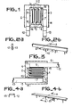
- the dielectric films 1 respectively covered with metallic layers 2 are offset with respect to each other, the layers of the same rank (even and odd) being connected between them by lateral electrical connections such as 3 and 4.
- the conductive bars 5 and 6 are assembled on either side of the stack of metallized dielectric films using insulating adhesive layers such as 7 and 9, and of conductive adhesive layers such as 8 and 10. It is noted in this figure, that, to ensure better electrical contact between the lateral electrical connections 3 and 4 and the adhesive layers 8 and 10, these terminate in menisci 14 and 15 which correspond to the filling of the re-entrant dihedrons formed by the lateral electrical connections 3 and 4 and the supply bars 5 and 6.
- FIG. 2 a feed bar is shown substantially on scale 1.
- this bar is viewed from the front with its sets of connection lugs 12 and 13, while FIG. 2 b represents a section along AA in Figure 2 a-
- the configuration of the bar shown in Figures 1 and 2 corresponds to the so-called "vertical" configuration of said bar.
- FIG. 3 a second alternative embodiment of the power bars according to the invention is shown, corresponding to the so-called "horizontal" configuration.
- the same elements as those of the previous figures have the same references.
- the only difference in this FIG. 3 is constituted by the arrangement of the conductive bars 5 and 6.
- These conductive bars have their respective connection tabs 12 and 13 situated on the same side as the lateral electrical connections 3 and 4 to which they are respectively connected.
- the upper parts 16 and 17 conductive bars are located approximately the same height as the wafers of metallized dielectric films to which they are connected.
- FIG. 4a there is shown a view on scale approximately 1a of a feed bar as described in FIG. 3.
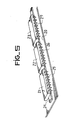
- This feed bar is of very flat shape, which makes it possible to use it in particular as shown in FIG. 5 for supplying integrated circuits such as 21, 22, 23 arranged on a printed board 20.
- the power bar 24 conforms to that described in FIGS. 3 and 4, can be housed between the connection tabs such as 25, 26 and 27 of said integrated circuits.
- connection tabs such as 25, 26 and 27 of said integrated circuits.
- EXAMPLE A polyethylene terephthalate film, with a dielectric constant of 3.2, is coated with a layer of vacuum-deposited aluminum of thickness substantially equal to 200 Angstroems, representing a square resistance of approximately 1.5 ohm . This film is cut into strips approximately 5 mm wide. On each of these strips, a small margin was made by removing the metal layer on one of the sides. The metallized films are then stacked according to the technique described in French patent 903,040, then the lateral electrical connections are made by spraying metal. After cooling, the stacks thus produced are cut into pieces of approximately 20 cm in length. Two metallic copper bars having lateral connection tabs regularly spaced along their length, and previously tinned, are then assembled with the stack produced above. To achieve this assembly, the metal bars are screen-printed with a single-component conductive epoxy adhesive containing 60% pure silver. After the glue has dried and polymerized, the feed bar is then subjected to the marking operation and is ready for use.
- the measurement of the resistance per unit length of the power bar according to the invention is for the 6 samples previously used between 0.21 and 0.22 milliohm per centimeter. Since the copper used has a resistivity of 0.017 ohm x square millimeter per millimeter, the theoretical resistance of these bars is equal to 0.21 milliohm per centimeter. It is therefore quite remarkable that the power bars according to the invention do not cause disturbances in the value of the resistance of the conductive bars used.
- the characteristic impedance of the bars measured using a pulse generator with a rise time of less than 5 nanoseconds made it possible to find an average characteristic impedance on the 6 samples mentioned above equal to 0, 31 ohm, the corresponding theoretical calculated value being 0.22 ohm.
- power bar (or “bus-bar” according to the English name) has generally been used. Saxon). It is obvious that this term in no way limits the function of these bars to a means of connection of a supply voltage source to a plurality of circuits. On the contrary, it designates a means of connecting any generator (source) of a continuous or alternating electrical signal, analog or digital to any receiver using this signal.
Landscapes
- Engineering & Computer Science (AREA)
- Microelectronics & Electronic Packaging (AREA)
- Fixed Capacitors And Capacitor Manufacturing Machines (AREA)
- Structure Of Printed Boards (AREA)
- Insulated Conductors (AREA)
Abstract
Barre d'alimentation de faible impédance caractéristique pour la transmission d'un signal électrique d'une source à une pluralité de récepteurs, ladite barre d'alimentation comportant notamment deux barres conductrices (5, 6) véhiculant le signal, séparées par des moyens diélectriques. Selon l'invention, les moyens diélectriques sont constitués par un empilement de films diélectriques métallisés formant un ensemble de 2 n films diélectriques (1), identiques ou différents, séparés par 2 n couches métalliques (2), les couches métalliques de rang pair et impair étant respectivement reliées entre elles latéralement par des connexions électriques (3, 4), les barres conductrices (5, 6) étant fixées de part et d'autre de l'empilement et reliées électriquement, respectivement à l'une des connexions électriques latérales (3, 4).
Description
La présente invention concerne des barres d'alimentation de faible impédance caractéristique pour la transmission d'un signal électrique d'une source à une pluralité de récepteurs, ladite barre d'alimentation comportant notamment deux barres conductrices véhiculant le courant séparées par des moyens diélectriques.The present invention relates to power bars of characteristic low impedance for the transmission of an electrical signal from a source to a plurality of receivers, said power bar comprising in particular two conductive bars carrying the current separated by dielectric means.
De telles barres d'alimentation, connues également sous l'appellation anglo-saxonne "bus-bar", sont utilisées depuis fort longtemps notamment dans les systèmes d'alimentation des circuits électriques d'ordinateur.Such power bars, also known by the Anglo-Saxon name "bus-bar", have been used for a very long time in particular in power systems for computer electrical circuits.
De telles lignes d'alimentation ont été réalisées dans le passé pour se substituer aux câbles coaxiaux beaucoup trop encombrants dans les circuits miniaturisés. Afin de réaliser le découplage nécessaire entre les différents circuits d'utilisation, il a déjà été proposé de connecter en parallèle sur la ligne des capacités afin d'augmenter le découplage.Such supply lines have been made in the past to replace coaxial cables that are too bulky in miniaturized circuits. In order to achieve the necessary decoupling between the different usage circuits, it has already been proposed to connect in parallel on the capacity line in order to increase the decoupling.
Toutefois, le montage de ces capacités en parallèle sur la ligne rend très difficiles les opérations de maintenance de celle-ci, ainsi que les problèmes de montage.However, mounting these capacities in parallel on the line makes it very difficult to maintain them, as well as mounting problems.
Il a été proposé dans le brevet américain 3 189 847 d'utiliser des barres d'alimentation constituées de deux barres conductrices séparées par un diélectrique dont les pertes augmentent avec la fréquence, tel qu'un matériau ferromagnétique qui a la propriété d'être conducteur aux basses fréquences ou en courant continu mais qui atténue très rapidement tous les signaux hautes fréquences. De cette façon, on évite la propagation sur la barre d'alimentation de signaux impulsionnels de fréquence élevée qui pourraient perturber le fonctionnement des circuits connectés sur ladite barre d'alimentation.It has been proposed in American patent 3,189,847 to use power bars consisting of two conductive bars separated by a dielectric whose losses increase with frequency, such as a ferromagnetic material which has the property of being conductive at low frequencies or direct current but which very quickly attenuates all high frequency signals. In this way, the propagation on the power bar of high frequency impulse signals is avoided which could disturb the operation of the circuits connected to said power bar.
Toutefois, un tel système présente l'inconvénient d'utiliser un matériau très particulier, relativement couteux et possédant de mauvaises propriétés mécaniques. En effet, un tel matériau ferromagnétique est généralement cassant et les barres d'alimentation obtenues selon la technique décrite dans ce brevet sont des barres rigides et d'épaisseur relativement importante. De plus, la transmission des signaux hautes fréquences avec une telle barre est impossible, compte tenu de la conception de celle-ci. Plus récemment, il a été proposé dans le brevet américain 3 312 870 de réaliser ces barres d'alimentation à l'aide de deux barres conductrices séparées par un matériau diélectrique ayant une constante diélectrique très élevée. Le matériau à haute constante diélectrique est obtenu à l'aide d'un empilement de plaques métalliques revêtues d'un film isolant d'oxyde obtenu par anodisation, les plaques étant assemblées les unes aux autres à l'aide d'une couche adhésive. Un tel dispositif est cependant peu facile à réaliser du fait de l'anodisation nécessaire des plaques métalliques et de leur épaisseur relativement importante ce qui, pour des capacités élevées, conduirait à une épaisseur totale des barres d'alimentation inacceptable.However, such a system has the disadvantage of using a very specific material, relatively expensive and having poor mechanical properties. Indeed, such a ferromagnetic material is generally brittle and the feed bars obtained according to the technique described in this patent are rigid bars and of relatively large thickness. In addition, the transmission of high frequency signals with such a bar is impossible, given the design thereof. More recently, it has been proposed in American patent 3,312,870 to produce these power bars using two conductive bars separated by a dielectric material having a very high dielectric constant. The material with a high dielectric constant is obtained using a stack of metal plates coated with an oxide insulating film obtained by anodization, the plates being joined to each other using an adhesive layer. Such a device is however not very easy to produce due to the necessary anodization of the metal plates and their relatively large thickness which, for high capacities, would lead to an unacceptable total thickness of the power bars.
Plus récemment, il a été proposé dans le brevet français 2 438 933 d'utiliser, non pas simplement un film diélectrique adhésif interposé entre les deux barres d'alimentation, mais de remplacer ledit film diélectrique adhésif par des pastilles successives de céramique à haute constante diélectrique. Une solution tout à fait identique avait d'ailleurs déjà été proposée par la Demanderesse dans le brevet américain 3 778 735. L'utilisation de matériau céramique à haute constante diélectrique présente cependant l'inconvénient d'introduire des pertes diélectriques et par conséquent une résistance série qui, aux fréquences élevées, dégrade l'impédance caractéristique des lignes ainsi réalisées et n'assure donc pas une bonne transmission de l'information.More recently, it has been proposed in French patent 2,438,933 to use, not simply an adhesive dielectric film interposed between the two supply bars, but to replace said adhesive dielectric film with successive pellets of high constant ceramic dielectric. A completely identical solution had already been proposed by the Applicant in American patent 3,778,735. The use of ceramic material with a high dielectric constant, however, has the disadvantage of introducing dielectric losses and therefore resistance. series which, at high frequencies, degrades the characteristic impedance of the lines thus produced and therefore does not ensure good transmission of information.
Tous les systèmes connus proposés jusqu'à ce jour, tels que ceux décrits ci-dessus, présentent cependant divers inconvénients :
- il existe en effet deux problèmes à résoudre lorsque l'on veut réaliser des barres d'alimentation à faible impédance caractéristique et sans pertes aux hautes fréquences. Ces barres doivent avoir la plus forte capacité répartie possible afin d'obtenir une très faible impédance caractéristique et posséder une épaisseur aussi réduite que possible afin de prendre le minimum de place dans les circuits utilisant ces barres d'alimentation.
- there are in fact two problems to be solved when it is desired to produce power bars with low characteristic impedance and without losses at high frequencies. These bars must have the highest distributed capacity possible in order to obtain a very low characteristic impedance and have a thickness as small as possible in order to take up the minimum space in the circuits using these power bars.
Lorsqu'on veut alimenter par exemple quelques circuits intégrés disposés sur un circuit imprimé, la barre d'alimentation ne doit bien entendu pas avoir une largeur excessive comparée à la largeur des boîtiers desdits circuits intégrés. Or, si l'on veut réaliser des barres d'alimentation ayant une très forte capacité, on peut soit réaliser des barres de grande largeur avec une seule couche de film diélectrique très mince interposé entre les barres d'alimentation, soit réaliser une barre de la façon décrite dans le brevet américain 3 312 870.When it is desired to supply, for example, a few integrated circuits arranged on a printed circuit, the power bar must of course not have an excessive width compared to the width of the boxes of said integrated circuits. However, if it is desired to produce supply bars having a very high capacity, it is possible either to produce large width bars with a single layer of very thin dielectric film interposed between the supply bars, or to produce a supply bar as described in US Patent 3,312,870.
Dans le premier cas, lesdites barres d'alimentation sont trop encombrantes et trop fragiles. En effet, les barres conductrices, généralement métalliques, ont un état de surface assez approximatif c'est-à-dire qu'il existe par endroit des parties saillantes métalliques de quelques microns d'épaisseur. Lorsqu'on assemble les deux barres conductrices à l'aide du film diélectrique adhésif, ces parties saillantes percent ledit diélectrique et la barre est en court-circuit.In the first case, said feed bars are too bulky and too fragile. In fact, the conductive bars, generally metallic, have a fairly approximate surface state, that is to say that there are metallic protrusions a few microns thick in places. When the two conductive bars are assembled using the adhesive dielectric film, these projecting parts pierce said dielectric and the bar is short-circuited.
Dans le second cas, les barres d'alimentation ainsi réalisées ont une épaisseur trop importante pour être utilisées dans certaines applications, notamment lorsqu'on veut placer lesdites barres sous les boîtiers des circuits intégrés du type DIL, entre les "pattes" desdits circuits intégrés.In the second case, the power bars thus produced are too thick to be used in certain applications, especially when it is desired to place said bars under the housings of integrated circuits of the DIL type, between the "tabs" of said integrated circuits. .
Par conséquent, il n'existe pas à l'heure actuelle de barres d'alimentation possédant une certaine souplesse, une impédance caractéristique très faible et une épaisseur réduite.Consequently, at the present time there are no power bars having a certain flexibility, a very low characteristic impedance and a reduced thickness.
Les barres d'alimentation selon l'invention ne possèdent pas les inconvénients des barres d'alimentation décrites ci-dessus et répondent au problème posé.The power bars according to the invention do not have the drawbacks of the power bars described above and respond to the problem posed.
Dans ce but, les barres d'alimentation selon l'invention sont caractérisées en ce que lesdits moyens diélectriques sont constitués par un empilement de films diélectriques métallisés formant un ensemble de 2 n films diélectriques, identiques ou différents, séparés par 2 n couches métalliques, les couches métalliques de rangs pair et impair étant respectivement reliées entre elles latéralement par des connexions électriques, les barres conductrices étant fixées de part et d'autre de l'empilement et reliées électriquement, respectivement à l'une des connexions électriques latérales. Les films métallisés peuvent être recouverts de métal sur l'une ou les deux faces. Dans ce dernier cas, on retrouvera dans l'empilement des couches métalliques constituées par deux couches superposées qui seront donc reliées électriquement entre elles par contact.For this purpose, the supply bars according to the invention are characterized in that said dielectric means consist of a stack of metallized dielectric films forming a set of 2 n dielectric films, identical or different, separated by 2 n metallic layers, the metallic layers of even and odd rows being respectively connected to each other laterally by electrical connections, the conductive bars being fixed on either side of the stack and connected electrically, respectively to one of the lateral electrical connections. Metallized films can be covered with metal on one or both sides. In the latter case, there will be found in the stack of metal layers formed by two superimposed layers which will therefore be electrically connected to each other by contact.
De préférence, on interposera entre l'empilement et chacune des barres conductrices des moyens formant coussin, dont le but est d'éviter avant tout une détérioration des couches de l'empilement. De préférence, l'épaisseur desdits coussins sera supérieure ou égale à 10 microns. Ces coussins pourront être constitués soit d'un adhésif tel qu'une colle époxy, un isocyanate, un polyuréthane ou un mélange de ceux-ci avec leurs durcisseurs respectifs (colles mono ou bi- composants), cet adhésif étant isolant au conducteur, soit d'une couche électriquement inactive, formée d'un film diélectrique souple.Preferably, cushioning means will be interposed between the stack and each of the conductive bars, the aim of which is above all to prevent deterioration of the layers of the stack. Preferably, the thickness of said cushions will be greater than or equal to 10 microns. These cushions may consist of either an adhesive such as an epoxy adhesive, an isocyanate, a polyurethane or a mixture of these with their respective hardeners (mono or two-component adhesives), this adhesive being insulating to the conductor, or an electrically inactive layer formed of a flexible dielectric film.
Les moyens formant coussin peuvent remplir la double fonction d'une part de permettre l'assemblage entre l'empilement de films diélectriques et les barres conductrices, et d'autre part d'éviter un contact direct entre les films métallisés et lesdites barres conductrices, afin d'éviter les blessures mécaniques de l'un par l'autre. Dans ce but, on utilisera de préférence un adhésif qui suivant les cas, par exemple la forme de la barre d'alimentation réalisée, sera isolant ou conducteur.The cushion-forming means can fulfill the dual function on the one hand of allowing assembly between the stack of dielectric films and the conductive bars, and on the other hand of avoiding direct contact between the metallized films and said conductive bars, in order to avoid mechanical injuries from each other. For this purpose, an adhesive will preferably be used which, depending on the case, for example the shape of the supply bar produced, will be insulating or conductive.
Comme adhésif conducteur, on pourra utiliser soit des vernis conducteurs soit des colles conductrices. La nature conductrice de ces vernis ou colles est généralement donnée par la présence d'une poudre métallique en quantité assez importante dans ceux-ci. Géne- ralement, la poudre métallique est de l'argent, connu pour ses très bonnes propriétés conductrices.As conductive adhesive, either conductive varnishes or conductive glues can be used. The conductive nature of these varnishes or glues is generally given by the presence of a metal powder in fairly large quantity therein. Generally, the metal powder is silver, known for its very good conductive properties.
Concernant les colles isolantes, on pourra utiliser tous types de colles bien connues de l'homme de l'art, mono ou bi-composant. En particulier, on pourra utiliser les colles du type polyuréthane et/ou époxy.Regarding insulating adhesives, all types of adhesives well known to those skilled in the art, one or two-component may be used. In particular, adhesives of the polyurethane and / or epoxy type may be used.
Dans le cas où les moyens formant coussin sont constitués par une couche électriquement inactive, formée d'un film diélectrique souple, celui-ci pourra être identique ou différent de l'un des diélectriques de l'empilement. Il sera de préférence choisi dans la même famille, décrite ci-après.In the case where the cushion-forming means consist of an electrically inactive layer, formed of a flexible dielectric film, this may be identical to or different from one of the dielectrics of the stack. It will preferably be chosen from the same family, described below.
Ce film sera rendu solidaire de l'empilement soit à l'aide d'un adhésif, soit à l'aide des connexions électriques latérales : celles-ci étant généralement obtenues par projection de métal en fusion, le film diélectrique est ainsi englobé dans l'empilement par le métal projeté.This film will be made integral with the stack either using an adhesive or using the lateral electrical connections: these are generally obtained by spraying molten metal, the dielectric film is thus included in the stacked by projected metal.
La partie supérieure de ce film sera rendue solidaire des barres conductrices, généralement à l'aide d'un adhésif tel que cela a été défini ci-dessus.The upper part of this film will be made integral with the conductive bars, generally using an adhesive as defined above.
D'une façon générale, et si l'on désire rendre la barre d'alimentation selon l'invention plus rigide, on pourra introduire dans l'empilement m couches d'adhésif, disposées entre les 2 n couches de films métallisés, m étant inférieur ou égal à 2 n - 1. Suivant le résultat désiré, on pourra faire varier m de 1 à 2 n -1. L'épaisseur de l'adhésif, choisi de préférence parmi les adhésifs courants disponibles dans le commerce, tels que décrits ci-dessus, variera généralement entre 0,2 et 2 microns.In general, and if it is desired to make the feed bar according to the invention more rigid, it is possible to introduce into the stack m layers of adhesive, arranged between the 2 n layers of metallized films, m being less than or equal to 2 n - 1. Depending on the desired result, we can vary m from 1 to 2 n -1. The thickness of the adhesive, preferably chosen from common commercially available adhesives, as described above, will generally vary between 0.2 and 2 microns.
De telles barres d'alimentation présentent des avantages importants par rapport aux barres d'alimentation connues, y compris celles comportant deux barres conductrices séparées par un film diélectrique adhésif. En effet, les barres d'alimentation selon l'invention possèdent la propriété d'être auto-cicatrisables.Such power bars have significant advantages over known power bars, including those having two conductive bars separated by an adhesive dielectric film. In fact, the power bars according to the invention have the property of being self-healing.
Le phénomène d'auto-cicatrisation est le suivant : lorsque le film diélectrique possède des défauts encore appelés "points conducteur", la mise sous tension de la barre conductrice, c'est-à-dire l'apparition d'une différence de potentiel entre les deux barres conductrices, provoque la volatilisation des parties d'armature métallisée en regard du point conducteur, sans perforation du diélectrique. De cette façon, la barre d'alimentation est malgré tout utilisable, aucun court-circuit n'apparaissant entre les barres conductrices.The phenomenon of self-healing is as follows: when the dielectric film has defects also called "conductive points", the tensioning of the conductive bar, that is to say the appearance of a potential difference between the two conductive bars, causes the volatilization of the parts of metallic reinforcement opposite the conductive point, without perforation of the dielectric. In this way, the power bar can still be used, no short-circuit appearing between the busbars.
Au contraire, dans le cas où l'on utilise un diélectrique, adhésif ou non, entre deux barres conductrices jouant le rôle d'armatures comme cela est décrit dans l'art antérieur, lorsque le diélectrique présente un défaut, on constate qu'à la mise sous tension de la barre, il y a perforation du diélectrique aux endroits correspondant aux points conducteurs lorsque la tension devient assez élevée : il y alors court-circuit de ladite barre d'alimentation. Les barres d'alimentation selon l'invention possèdent donc le très grand avantage d'une fiabilité accrue par rapport aux barres d'alimentation du même type connues jusqu'à ce jour.On the contrary, in the case where a dielectric, adhesive or not, is used between two conductive bars playing the role of reinforcements as described in the prior art, when the dielectric has a defect, it is found that when the bar is energized, there is a perforation of the dielectric at the points corresponding to the conductive points when the voltage becomes high enough: there is then a short circuit of said power bar. The power bars according to the invention therefore have the very great advantage of increased reliability compared to the power bars of the same type known to date.
De plus, les films métallisés utilisés pour réaliser les barres selon l'invention permettant à ladite barre de subir un gradient de tension élevé, le diélectrique utilisé peut avoir une épaisseur faible, ce qui se traduit par une augmentation importante de la capacité c'est-à-dire que la barre d'alimentation selon l'invention possède une impédance caractéristique très faible. On peut en effet dans le cadre de l'invention utiliser des films diélectriques d'épaisseur de l'ordre de 1,5 micron tout en ayant une tension de service supérieure à 100 volts.In addition, the metallized films used to make the bars according to the invention allowing said bar to undergo a high voltage gradient, the dielectric used can have a low thickness, which results in a significant increase in capacity. ie the power bar according to the invention has a very low characteristic impedance. In the context of the invention, it is indeed possible to use dielectric films with a thickness of the order of 1.5 microns while having an operating voltage greater than 100 volts.
Au contraire, dans le cas d'armatures solides, le film diélectrique doit avoir une épaisseur d'au moins 20 microns pour que la barre d'alimentation possède une fiabilité d'utilisation correcte. Dans ces conditions, la capacité par unité de longueur de ladite barre est bien évidemment beaucoup plus faible, ce qui se traduit par une impédance caractéristique beaucoup plus élevée et une barre d'alimentation mal adaptée au problème à résoudre.On the contrary, in the case of solid reinforcements, the dielectric film must have a thickness of at least 20 microns so that the supply bar has a correct reliability of use. Under these conditions, the capacity per unit length of said bar is obviously much lower, which results in a much higher characteristic impedance and a power bar ill-suited to the problem to be solved.
L'impédance caractéristique des barres selon l'invention reste faible même aux très hautes fréquences, contrairement à celles faisant usage d'un matériau céramique à forte constante diélectrique. En effet, dans le cas de matériau céramique, les pertes diélectriques en haute fréquence introduisent une résistance série dans le circuit qui dégrde l'impédance caractéristique des lignes ainsi réalisées.The characteristic impedance of the bars according to the invention remains low even at very high frequencies, unlike those using a ceramic material with a high dielectric constant. Indeed, in the case of ceramic material, the dielectric losses at high frequency introduce a series resistance in the circuit which degrades the characteristic impedance of the lines thus produced.
De plus, contrairement aux barres connues de l'art antérieur, les barres d'alimentation selon l'invention peuvent être coupées à la longueur voulue sans aucun risque de court-circuit entre les barres conductrices. En effet, la présence des coussins permet une séparation suffisante des barres entre-elles.In addition, unlike the bars known in the prior art, the supply bars according to the invention can be cut to the desired length without any risk of short circuit between the conductive bars. Indeed, the presence of the cushions allows sufficient separation of the bars from one another.
Les barres d'alimentation selon l'invention peuvent être utilisées, ainsi que cela sera décrit par la suite, soit verticalement, c'est-à-dire disposées entre les circuits intégrés de la carte imprimée, soit horizontalement, c'est-à-dire sous les circuits intégrés entre leurs pattes de connexion.The power bars according to the invention can be used, as will be described later, either vertically, that is to say arranged between the integrated circuits of the printed circuit board, or horizontally, that is to say - say under the integrated circuits between their connection lugs.
Lorsqu'on utilise ces barres d'alimentation verticalement, les barres conductrices ont leurs connexions destinées à être fixées dans les trous des circuits imprimés, situées du même côté d'une connexion électrique latérale. Dans ce but, lesdites barres conductrices seront donc fixées de part et d'autre de l'empilement de films diélectriques métallisés à l'aide de deux adhésifs différents, la partie de la barre conductrice située à proximité de la connexion électrique latérale à laquelle elle doit être reliée étant fixée à l'aide d'un adhésif conducteur de l'électricité, tandis que l'autre partie de la barre conductrice située en regard de la connexion électrique à ',laquelle elle ne doit pas être reliée sera fixée à l'aide d'un adhésif ou film adhésivé non conducteur de l'électricité.When these power bars are used vertically, the conductive bars have their connections intended to be fixed in the holes of the printed circuits, located on the same side of a lateral electrical connection. For this purpose, said conductive bars will therefore be fixed on either side of the stack of metallized dielectric films using two different adhesives, the part of the conductive bar located near the lateral electrical connection to which it must be connected being fixed with an electrically conductive adhesive, while the other part of the conductive bar located opposite the electrical connection to ' , which it must not be connected will be fixed to the using an electrically non-conductive adhesive or film.
De préférence, afin de renforcer la résistance mécanique desdites barres d'alimentation, on disposera également de l'adhésif, conducteur ou non conducteur, à l'intérieur des dièdres rentrants formés par les barres d'alimentation et les connexions électriques latérales reliant entre-eux les films métallisés. Ceci est particulièrement nécessaire à l'intérieur des dièdres situés du côté ou la barre conductrice doit être connectée sur le circuit imprimé.Preferably, in order to reinforce the mechanical resistance of said supply bars, there will also be adhesive, conductive or non-conductive, inside the re-entrant dihedrons formed by the supply bars and the lateral electrical connections connecting between them metallic films. This is special rely necessary inside the dihedrons located on the side where the busbar must be connected to the printed circuit.
Comme film diélectrique utilisable dans le cadre de l'invention, on pourra utiliser tout film diélectrique ayant des propriétés convenables, bien connues de l'homme de l'art. De préférence, on utilisera les films diélectriques courants tels que le papier, les polyoléfines et en particulier le polypropylène et le polyéthylène, le polycarbonate, le polysulfone, le polystyrène, ou les polyesters tels que le polytérephtalate d'éthylène, ceux-ci étant généralement les films préférés dans le cadre de la présente invention (en particulier à cause de leur forte constante diélectrique). On peut également utiliser d'autres films diélectriques tels que les films de polyamide (nylon 6, nylon 6,6, ...), polyimide, polyamide-imide, polytétrafluoroéthylène, polyfluorure de vinylidène, etc. L'épaisseur du film utilisé sera aussi faible que possible, puisque la capacité de la barre augmente lorsque l'épaisseur du diélectrique diminue. Celle-ci sera généralement inférieure à 20 microns, et de préférence inférieure à 5 microns. On choisira de préférence un diélectrique ayant un angle de perte à 25°C à la fréquence de 1 KHz tel que la tangente de cet angle, appelée couramment tangente 6 soit dans tous les cas inférieure ou égale à 2 x 10⁻² et de préférence inférieure à 5 x 10⁻³.As a dielectric film which can be used in the context of the invention, any dielectric film having suitable properties well known to those skilled in the art may be used. Preferably, common dielectric films such as paper, polyolefins and in particular polypropylene and polyethylene, polycarbonate, polysulfone, polystyrene, or polyesters such as polyethylene terephthalate will be used, these being generally the films preferred in the context of the present invention (in particular because of their high dielectric constant). It is also possible to use other dielectric films such as polyamide films (
D'une manière générale, on choisira le type de diélectrique, son épaisseur, etc... de telle manière que l'on obtienne une capacité par centimètre de longueur de barres d'alimentation supérieure à 20 nanofarads. On considère en effet que cette valeur est une valeur minimale pour obtenir des barres d'alimentation à faible constante répartie permettant de transmettre tous les signaux, du continu jusqu'à plusieurs centaines de MHz. C'est ce qui rend la réalisation de ces barres d'alimentation particulièrement délicates.In general, the type of dielectric, its thickness, etc., will be chosen so that a capacity per centimeter of length of power bars greater than 20 nanofarads is obtained. It is in fact considered that this value is a minimum value in order to obtain power bars with a low distributed constant enabling all the signals to be transmitted, from continuous to several hundred MHz. This is what makes the production of these power bars particularly delicate.
Le métal utilisable pour métalliser la surface du film diélectrique sera de préférence le zinc, l'aluminium, l'argent , l'or ou le cuivre. L'épaisseur de la couche métallique déposée sur le film diélectrique sera telle que la résistance "carrée" du film métallisé varie entre 0,5 ohm et 5 ohms. Par résistance "carrée", on entend la résistance de la couche métallique d'un carré de film métallisé de, par exemple, un centimètre de côté.The metal which can be used to metallize the surface of the dielectric film will preferably be zinc, aluminum, silver, gold or copper. The thickness of the metallic layer deposited on the dielectric film will be such that the "square" resistance of the metallized film varies between 0.5 ohm and 5 ohms. By "square" resistance is meant the resistance of the metallic layer of a square of metallized film of, for example, a centimeter of side.
En effet, au delà d'une résistance carrée de 5 ohms, on constate que le dépôt métallique est si mince qu'il se produit des inégalités dans la répartition du métal, lesdites inégalités engendrant des défauts importants dans les barres d'alimentation obtenues avec ces films. Pour une résistance carrée inférieure à 0,5 ohm, on considère généralement que l'épaisseur du dépôt métallique est trop importante pour rendre économiquement intéressante la réalisation de barres d'alimentation par ces procédés. De plus, un dépôt épais est difficile à réaliser et la barre d'alimentation obtenue avec un dépôt épais perd sa faculté d'auto-cicatrisation.Indeed, beyond a square resistance of 5 ohms, it can be seen that the metal deposit is so thin that there are inequalities in the distribution of the metal, said inequalities causing significant defects in the power bars obtained with this movies. For a square resistance less than 0.5 ohm, it is generally considered that the thickness of the metal deposit is too great to make it economically advantageous to produce supply bars by these methods. In addition, a thick deposit is difficult to achieve and the power bar obtained with a thick deposit loses its faculty of self-healing.
Les barres conductrices seront généralement réalisées en matériau très conducteur, tel que le cuivre. De préférence, ce matériau conducteur sera recouvert d'une couche d'étain, déposée avant ou après découpe desdites barres. Cet étamage sera réalisé, de manière connue en soi, soit par voie chimique soit par voie électrolytique. L'épaisseur de la couche d'étain sera de préférence 20 microns. Lorsque cet étamage est réalisé avant découpe des barres, on constate que la couche d'étain subit un fluage au cours de la découpe et vient ainsi protéger le bord latéral de la barre conductrice.The conductive bars will generally be made of very conductive material, such as copper. Preferably, this conductive material will be covered with a layer of tin, deposited before or after cutting of said bars. This tinning will be carried out, in a manner known per se, either chemically or electrolytically. The thickness of the tin layer will preferably be 20 microns. When this tinning is carried out before cutting the bars, it can be seen that the tin layer undergoes creep during cutting and thus protects the lateral edge of the conductive bar.
En pratique, on réalisera généralement des barres d'alimentation comportant entre quatre et vingt couches de film diélectrique métallisé, les autres éléments de la barre étant choisis de telle sorte que l'épaisseur totale de celle-ci reste inférieure à 3 mm. Ces données correspondent au meilleur mode de réalisation de l'invention.In practice, power bars will generally be produced comprising between four and twenty layers of metallized dielectric film, the other elements of the bar being chosen so that the total thickness thereof remains less than 3 mm. These data correspond to the best embodiment of the invention.
Pour réaliser les barres d'alimentation selon l'invention, on réalise tout d'abord l'empilement des films diélectriques métallisés et leur assemblage par projection latérale de métal. Cette technique est en elle-même bien connue et décrite par exemple dans le brevet français N° 903 040. Les empilements ainsi réalisés sont ensuite découpés à la longueur voulue et assemblés avec les barres conductrices correspondantes. Celles-ci peuvent se présenter sous forme de rouleaux qui sont déroulés au cours de l'assemblage avec les empilements diélectriques, chaque barre étant au préalable revêtue d'une couche de colle aux endroits voulus, par exemple à l'aide d'un tambour muni d'un écran de soie qui permet le dépôt en continu de la colle par sérigraphie. Afin d'obtenir les viscosités nécessaires à l'utilisation du procédé de la sérigraphie, on ajustera la viscosité des colles utilisées par dilution plus ou moins importante dans un solvant approprié. Après assemblage sous pression des empilements et des -barres pendant un intervalle de temps suffisant pour permettre à la colle de polymériser, les barres d'alimentation selon l'invention sont alors prêtes à l'emploi.To produce the supply bars according to the invention, the stacking of the metallized dielectric films is first carried out and their assembly by lateral projection of metal. This technique is in itself well known and described for example in French patent N ° 903,040. The stacks thus produced are then cut to the desired length and assembled with the conduc bars. corresponding trices. These can be in the form of rolls which are unrolled during assembly with the dielectric stacks, each bar being previously coated with a layer of glue at the desired locations, for example using a drum. provided with a silk screen which allows the continuous deposit of the glue by screen printing. In order to obtain the viscosities necessary for the use of the screen printing process, the viscosity of the adhesives used will be adjusted by more or less dilution in an appropriate solvent. After pressure assemblies of the stacks and bars for a sufficient time interval to allow the glue to polymerize, the supply bars according to the invention are then ready for use.
On peut cependant, si cela s'avère nécessaire, procéder à un enrobage dans une résine appropriée des barres ainsi réalisées. Cette protection peut être également une peinture, un ruban thermo plastique ou adhésif, etc.However, if necessary, it is possible to coat the bars thus produced in an appropriate resin. This protection can also be a paint, a thermo-plastic or adhesive tape, etc.
L'invention sera mieux comprise à l'aide des exemples de réalisation suivants, donnés à titre non limitatif, conjointement avec les figures qui représentent :
- - la figure 1, une première variante de réalisation des barres d'alimentation selon l'invention, correspondant à une position verticale de la barre,
- - la figure 2 représente une vue d'ensemble de la barre d'alimentation de la figure 1,
- - la figure 3 représente une deuxième variante de réalisation de l'invention, correspondant à une position horizontale de la barre,
- - la figure 4 est une vue d'ensemble d'une barre selon la figure 3,
- - la figure 5 représente un exemple d'utilisation d'une barre telle que décrite sur les figures 3
et 4, implantée sur un circuit imprimé entre les pattes de connexion de circuits intégrés.
- FIG. 1, a first alternative embodiment of the supply bars according to the invention, corresponding to a vertical position of the bar,
- FIG. 2 represents an overall view of the supply bar of FIG. 1,
- FIG. 3 represents a second variant embodiment of the invention, corresponding to a horizontal position of the bar,
- FIG. 4 is an overall view of a bar according to FIG. 3,
- - Figure 5 shows an example of the use of a bar as described in Figures 3 and 4, located on a printed circuit between the connection tabs of integrated circuits.
Sur la figure 1, les films diélectriques 1 recouverts respectivement de couches métalliques 2 sont décalés les uns par rapport aux autres, les couches d'un même rang (pair et impair) étant reliées entre elles par des connexions électriques latérales telles que 3 et 4. Les barres conductrices 5 et 6 sont assemblées de part et d'autre de l'empilement des films diélectriques métallisés à l'aide de couches adhésives isolantes telles que 7 et 9, et de couches adhésives conductrices telles que 8 et 10. On remarque sur cette figure, que, pour assurer un meilleur contact électrique entre les connexions électriques latérales 3 et 4 et les couches adhésives 8 et 10, celles-ci se terminent par des ménisques 14 et 15 qui correspondent au remplissage des dièdres rentrants formés par les connexions électriques latérales 3 et 4 et les barres d'alimentation 5 et 6.In FIG. 1, the dielectric films 1 respectively covered with
Sur cette figure, l'ensemble de la barre conductrice, exceptées les pattes de connexion 12 et 13, a été noyé dans une résine 11 dont le pourtour est représenté en pointillé sur la figure.In this figure, the whole of the conductive bar, except for the connection lugs 12 and 13, has been embedded in a resin 11, the periphery of which is shown in dotted lines in the figure.
Sur la figure 2, est représentée une barre d'alimentation sensiblement à l'échelle 1. Sur la figure 2 , cette barre est vue de a face avec ses ensembles de pattes de connexion 12 et 13, tandis que la figure 2b représente une coupe selon AA de la figure 2 a- La configuration de la barre représentée sur les figures 1 et 2 correspond à la configuration dite "verticale" de ladite barre.In FIG. 2, a feed bar is shown substantially on scale 1. In FIG. 2, this bar is viewed from the front with its sets of connection lugs 12 and 13, while FIG. 2 b represents a section along AA in Figure 2 a- The configuration of the bar shown in Figures 1 and 2 corresponds to the so-called "vertical" configuration of said bar.
Sur la figure 3, est représentée une deuxième variante de réalisation des barres d'alimentation selon l'invention, correspondant à la configuration dite "horizontale". Sur cette figure, les mêmes éléments que ceux des figures précédentes portent les mêmes références. Par rapport à la figure l, la seule différence sur cette figure 3 est constituée par la disposition des barres conductrices 5 et 6. Ces barres conductrices ont leurs pattes de connexions respectives 12 et 13 situées du même côté que les connexions électriques latérales 3 et 4 auxquelles elles sont respectivement reliées. Dans cette configuration, on peut, sans que cela soit nécessaire, éviter l'utilisation de colles isolantes. Dans ce cas, il suffit de raccorder les barres conductrices selon la configuration représentée sur la figure, en prenant soin d'éviter le contact électrique entre les barres et les connexions électriques latérales 3 et 4. Dans ce but, les parties supérieures 16 et 17 des barres conductrices sont situées approximativement à la même hauteur que les tranches de films diélectriques métallisés auxquelles elles sont reliées.In Figure 3, a second alternative embodiment of the power bars according to the invention is shown, corresponding to the so-called "horizontal" configuration. In this figure, the same elements as those of the previous figures have the same references. Compared to FIG. 1, the only difference in this FIG. 3 is constituted by the arrangement of the
Sur la figure 4a, est représentée une vue à l'échelle 1 environ a d'une barre d'alimentation telle que décrite sur la figure 3. Cette barre d'alimentation est de forme très plate, ce qui permet de l'utiliser en particulier comme cela est montré sur la figure 5 pour alimenter des circuits intégrés tels que 21, 22, 23 disposés sur une carte imprimée 20. Dans une telle configuration, la barre d'alimentation 24 conforme à celle décrite sur les figures 3 et 4, peut venir se loger entre les pattes de connexion telles que 25, 26 et 27 desdits circuits intégrés. Une telle disposition est rendue facilement réalisable par la structure des barres selon l'invention.In FIG. 4a, there is shown a view on scale approximately 1a of a feed bar as described in FIG. 3. This feed bar is of very flat shape, which makes it possible to use it in particular as shown in FIG. 5 for supplying integrated circuits such as 21, 22, 23 arranged on a printed
EXEMPLE : Un film de polytérephtalate d'éthylène, de constante diélectrique relative 3,2, est revêtu d'une couche d'aluminium déposée sous vide d'épaisseur sensiblement égale à 200 Angstroems, représentant une résistance carrée d'environ 1,5 ohm. Ce film est découpé en bandelettes de 5 mm de largeur environ. Sur chacune de ces bandelettes, une petite marge a été réalisée par suppression de la couche métallique sur l'un des côtés. On réalise ensuite l'empilement des films métallisés selon la technique décrite dans le brevet français 903 040 puis l'on réalise les connexions électriques latérales par projection de métal. Après refroidissement, on découpe les empilements ainsi réalisés en morceaux d'environ 20 cm de longueur. Deux barres métalliques en cuivre possédant des pattes de connexion latérales régulièrement espacées sur leur longueur, et préalablement étamées, sont ensuite assemblées avec l'empilement réalisé ci-dessus. Pour réaliser cet assemblage, les barres métalliques sont recouvertes par sérigraphie d'une colle époxy conductrice mono- composant comportant 60% d'argent pur. Après séchage et polymérisation de la colle, la barre d'alimentation est ensuite soumise à l'opération de marquage et est prête à l'emploi.EXAMPLE: A polyethylene terephthalate film, with a dielectric constant of 3.2, is coated with a layer of vacuum-deposited aluminum of thickness substantially equal to 200 Angstroems, representing a square resistance of approximately 1.5 ohm . This film is cut into strips approximately 5 mm wide. On each of these strips, a small margin was made by removing the metal layer on one of the sides. The metallized films are then stacked according to the technique described in French patent 903,040, then the lateral electrical connections are made by spraying metal. After cooling, the stacks thus produced are cut into pieces of approximately 20 cm in length. Two metallic copper bars having lateral connection tabs regularly spaced along their length, and previously tinned, are then assembled with the stack produced above. To achieve this assembly, the metal bars are screen-printed with a single-component conductive epoxy adhesive containing 60% pure silver. After the glue has dried and polymerized, the feed bar is then subjected to the marking operation and is ready for use.
Des mesures électriques effectuées sur cette barre ont permis d'obtenir les résultats suivants :
- - Résistance d'isolement sous 10 volts : 75 000 Mégohms (mesure effectuée selon la norme NFC 93 050 article 1).
- - Capacité de la barre mesurant 23 cm de longueur : 690 nanofarads.
- - Tension de tenue (selon la norme NFC 93 050 article 2) : on applique une tension de 100 volts entre les deux barres conductrices par l'intermédiaire des connexions, pendant une minute sur 6 échantillons soumis à cet essai, on ne constate aucune perforation diélectrique ni phénomène d'effluve ni crépitements pendant toute la durée de l'essai. Autrement dit, aucun défaut n'est apparu au cours de cet essai. La résistance d'isolement après cet essai reste généralement sensiblement égale à celle de l'échantillon avant essai.
- - Insulation resistance under 10 volts: 75,000 Megohms (measurement made in accordance with NFC 93 050 article 1).
- - Capacity of the bar measuring 23 cm in length: 690 nanofarads.
- - Withstand voltage (according to NFC standard 93 050 article 2): a voltage of 100 volts is applied between the two busbars via the connections, for one minute on 6 samples subjected to this test, no perforation is observed dielectric neither phenomenon of emanation nor cracklings during all the duration of the test. In other words, no defect appeared during this test. The insulation resistance after this test generally remains substantially equal to that of the sample before test.
La mesure de la résistance par unité de longueur de la barre d'alimentation selon l'invention se situe pour les 6 échantillons précédemment utilisés entre 0,21 et 0,22 milliohm par centimètre. Le cuivre utilisé ayant une résistivité de 0,017 ohm x millimètre carré par millimètre, la résistance théorique de ces barres est égale à 0,21 milliohm par centimètre. Il est donc tout à fait remarquable que les barres d'alimentation selon l'invention n'apportent pas de perturbations dans la valeur de la résistance des barres conductrices utilisées.The measurement of the resistance per unit length of the power bar according to the invention is for the 6 samples previously used between 0.21 and 0.22 milliohm per centimeter. Since the copper used has a resistivity of 0.017 ohm x square millimeter per millimeter, the theoretical resistance of these bars is equal to 0.21 milliohm per centimeter. It is therefore quite remarkable that the power bars according to the invention do not cause disturbances in the value of the resistance of the conductive bars used.
Enfin, l'impédance caractéristique des barres mesurée à l'aide d'un générateur d'impulsions avec un temps de montée inférieur à 5 nanosecondes, a permis de trouver une impédance caractéristique moyenne sur les 6 échantillons mentionnés ci-dessus égale à 0,31 ohm, la valeur calculée théorique correspondante étant de 0,22 ohm.Finally, the characteristic impedance of the bars measured using a pulse generator with a rise time of less than 5 nanoseconds, made it possible to find an average characteristic impedance on the 6 samples mentioned above equal to 0, 31 ohm, the corresponding theoretical calculated value being 0.22 ohm.
On constate donc que les lignes ainsi réalisées ont une très faible impédance caractéristique, que leur procédé de réalisation apporte très peu de pertes (l'impédance caractéristique mesurée est peu différente de l'impédance caractéristique théorique).It can therefore be seen that the lines thus produced have a very low characteristic impedance, that their production method brings very few losses (the measured characteristic impedance is little different from the theoretical characteristic impedance).
A titre comparatif, l'impédance caractéristique de produits du même type couramment disponibles dans le commerce a été trouvée voisine de 2,5 ohms.By way of comparison, the characteristic impedance of products of the same type commonly available on the market has been found to be close to 2.5 ohms.
Dans l'exposé qui précède, on a généralement utilisé le terme de barre d'alimentation (ou "bus-bar" selon l'appellation anglo-saxonne). Il est bien évident que ce terme ne limite en aucune façon la fonction de ces barres à un moyen de connexion d'une source de tension d'alimentation à une pluralité de circuits. Il désigne au contraire un moyen de connexion d'un générateur (source) quelconque de signal électrique continu ou alternatif, analogique ou numérique à un récepteur quelconque utilisant ce signal.In the foregoing description, the term “power bar” (or “bus-bar” according to the English name) has generally been used. Saxon). It is obvious that this term in no way limits the function of these bars to a means of connection of a supply voltage source to a plurality of circuits. On the contrary, it designates a means of connecting any generator (source) of a continuous or alternating electrical signal, analog or digital to any receiver using this signal.
Claims (16)
Applications Claiming Priority (2)
| Application Number | Priority Date | Filing Date | Title |
|---|---|---|---|
| FR8025270A FR2495387A1 (en) | 1980-11-28 | 1980-11-28 | FEED BAR INCLUDING A STACK OF 2 N METAL LAYERS SEPARATED BY 2 N DIELECTRIC LAYERS |
| FR8025270 | 1980-11-28 |
Publications (2)
| Publication Number | Publication Date |
|---|---|
| EP0053531A1 true EP0053531A1 (en) | 1982-06-09 |
| EP0053531B1 EP0053531B1 (en) | 1984-08-22 |
Family
ID=9248444
Family Applications (1)
| Application Number | Title | Priority Date | Filing Date |
|---|---|---|---|
| EP81401783A Expired EP0053531B1 (en) | 1980-11-28 | 1981-11-10 | Feed bus made of a stack of 2 n dielectric layers disposed alternately with 2n metallic layers |
Country Status (5)
| Country | Link |
|---|---|
| US (1) | US4401844A (en) |
| EP (1) | EP0053531B1 (en) |
| BR (1) | BR8107696A (en) |
| DE (1) | DE3165709D1 (en) |
| FR (1) | FR2495387A1 (en) |
Cited By (1)
| Publication number | Priority date | Publication date | Assignee | Title |
|---|---|---|---|---|
| FR2530086A1 (en) * | 1982-07-09 | 1984-01-13 | Europ Composants Electron | Method of electrically connecting an interconnection bar |
Families Citing this family (16)
| Publication number | Priority date | Publication date | Assignee | Title |
|---|---|---|---|---|
| US4494170A (en) * | 1983-11-14 | 1985-01-15 | Rogers Corporation | Decoupling capacitor and method of manufacture thereof |
| US4532572A (en) * | 1983-11-14 | 1985-07-30 | Rogers Corporation | Decoupling capacitor and method of manufacture thereof |
| US4536826A (en) * | 1984-09-10 | 1985-08-20 | At&T Bell Laboratories | Snap-in bus bar |
| US4719541A (en) * | 1985-02-13 | 1988-01-12 | Fujitsu Limited | Electronic apparatus mounting structure |
| US5166867A (en) * | 1985-12-31 | 1992-11-24 | Fujitsu Limited | Bus bar for a circuit board |
| DE4031203A1 (en) * | 1990-10-04 | 1992-04-09 | Bosch Gmbh Robert | THICK LAYER HYBRID ARRANGEMENT WITH EXTERNAL CONTACTS |
| US5306874A (en) * | 1991-07-12 | 1994-04-26 | W.I.T. Inc. | Electrical interconnect and method of its manufacture |
| DE19507790C1 (en) * | 1995-03-06 | 1996-03-21 | Siemens Nixdorf Inf Syst | Current supply rail system with smoothing capacitors for dataprocessor |
| US5875091A (en) * | 1997-01-07 | 1999-02-23 | Siemens Nixdorf Informationssysteme Aktiengesellschaft | Busbars with filter capacitors |
| US6916990B2 (en) * | 2002-09-30 | 2005-07-12 | Teradyne, Inc. | High power interface |
| US20040154829A1 (en) * | 2003-01-31 | 2004-08-12 | Sass Forrest L. | Low inductance high capacitance power cable for connecting a power supply to an electrical load |
| JP4314513B2 (en) * | 2003-06-18 | 2009-08-19 | アイシン・エィ・ダブリュ株式会社 | Inverter noise remover |
| US20050109856A1 (en) * | 2003-11-25 | 2005-05-26 | Alexander James N.Iv | Method for preparing polymer electrosprays |
| JP4952123B2 (en) * | 2005-12-13 | 2012-06-13 | パナソニック株式会社 | Capacitor unit |
| US8643380B1 (en) * | 2010-07-15 | 2014-02-04 | Edward Herbert | Method and apparatus for reducing shock and arc-flash hazards in power distribution systems |
| DE102012222423B4 (en) * | 2012-12-06 | 2021-05-20 | Siemens Aktiengesellschaft | Device for the insulation of conductors |
Citations (2)
| Publication number | Priority date | Publication date | Assignee | Title |
|---|---|---|---|---|
| US3312870A (en) * | 1964-03-13 | 1967-04-04 | Hughes Aircraft Co | Electrical transmission system |
| US3520987A (en) * | 1968-08-05 | 1970-07-21 | Eldre Components | High capacity bus bar |
Family Cites Families (4)
| Publication number | Priority date | Publication date | Assignee | Title |
|---|---|---|---|---|
| US3189847A (en) * | 1961-05-29 | 1965-06-15 | Ibm | D. c. power distribution system |
| US3351876A (en) * | 1964-10-26 | 1967-11-07 | Hughes Aircraft Co | Electrical transmission system |
| FR2138403B1 (en) * | 1971-05-25 | 1976-12-03 | Europ Composants Electron | |
| US4236046A (en) * | 1978-10-10 | 1980-11-25 | Rogers Corporation | High capacitance bus bar |
-
1980
- 1980-11-28 FR FR8025270A patent/FR2495387A1/en active Granted
-
1981
- 1981-11-10 DE DE8181401783T patent/DE3165709D1/en not_active Expired
- 1981-11-10 EP EP81401783A patent/EP0053531B1/en not_active Expired
- 1981-11-24 US US06/324,608 patent/US4401844A/en not_active Expired - Fee Related
- 1981-11-28 BR BR8107696A patent/BR8107696A/en unknown
Patent Citations (2)
| Publication number | Priority date | Publication date | Assignee | Title |
|---|---|---|---|---|
| US3312870A (en) * | 1964-03-13 | 1967-04-04 | Hughes Aircraft Co | Electrical transmission system |
| US3520987A (en) * | 1968-08-05 | 1970-07-21 | Eldre Components | High capacity bus bar |
Cited By (1)
| Publication number | Priority date | Publication date | Assignee | Title |
|---|---|---|---|---|
| FR2530086A1 (en) * | 1982-07-09 | 1984-01-13 | Europ Composants Electron | Method of electrically connecting an interconnection bar |
Also Published As
| Publication number | Publication date |
|---|---|
| DE3165709D1 (en) | 1984-09-27 |
| FR2495387A1 (en) | 1982-06-04 |
| BR8107696A (en) | 1982-08-24 |
| US4401844A (en) | 1983-08-30 |
| EP0053531B1 (en) | 1984-08-22 |
| FR2495387B1 (en) | 1983-11-25 |
Similar Documents
| Publication | Publication Date | Title |
|---|---|---|
| EP0053531B1 (en) | Feed bus made of a stack of 2 n dielectric layers disposed alternately with 2n metallic layers | |
| EP0086922A1 (en) | Method of production of piezo-electric polymer transducers | |
| FR2475302A1 (en) | ELECTRIC INTERCONNECTION AND METHOD FOR PRODUCING THE SAME | |
| EP0006039B1 (en) | Method of interconnecting the connection terminals of electrical assemblies | |
| EP0201422A2 (en) | Integrable solid cell and process for its manufacture | |
| FR2882174A1 (en) | METHOD FOR MANUFACTURING A MICROELECTRONIC DEVICE WITH NON-CONTACT FUNCTIONING, IN PARTICULAR FOR ELECTRONIC PASSPORT | |
| EP0751556B1 (en) | Fabrication process for an interconnection substrate allowing to connect a die to a carrier substrate | |
| FR2503475A1 (en) | HIGH CAPACITY OMNIBUS BAR | |
| EP0040559B1 (en) | Piezoelectric convolution device using elastic waves | |
| FR2746985A1 (en) | Piezoelectric resonator for communication equipment filter or oscillator | |
| EP0197227A1 (en) | Electrical cable, especially for aerospatial use, with improved electrical characteristics | |
| EP0800211A1 (en) | Integrated circuit package | |
| FR2503473A1 (en) | HIGH CAPACITY OMNIBUS BAR AND MANUFACTURING METHOD THEREOF | |
| FR2891085A1 (en) | INCORPORATED CAPACITOR MODULE HAVING A MULTIPLE LAYER STRUCTURE. | |
| FR2632739A1 (en) | LOAD TRANSFER IMAGE FORMATION CARTRIDGE | |
| FR2495388A1 (en) | Electrical supply and signal bus=bar - uses metallic and dielectric films with conducting and non-conducting adhesives in high capacitance strip for printed circuit boards | |
| EP0626704B1 (en) | Apparatus for manufacturing of electrets | |
| EP0059206B1 (en) | Printed circuit and manufacturing process thereof | |
| EP0920035A1 (en) | Data transmission cable | |
| EP2681768A2 (en) | Process for monolithic series connection of the photovoltaic cells of a solar module and a photovoltaic module obtained by this process | |
| EP0586010A1 (en) | High frequency circuit device and method for making the same | |
| EP0120754A1 (en) | Polarized electronic component, and method for its manufacture | |
| EP0192523B1 (en) | Flexible electrical insulation material and method of manufacturing it | |
| EP0050547A1 (en) | Conducting link used in the transport of impulses of strong power, and method for its manufacture | |
| FR2515888A1 (en) | HIGH CAPACITANCE LAMINATED OMNIBUS BAR |
Legal Events
| Date | Code | Title | Description |
|---|---|---|---|
| PUAI | Public reference made under article 153(3) epc to a published international application that has entered the european phase |
Free format text: ORIGINAL CODE: 0009012 |
|
| AK | Designated contracting states |
Designated state(s): DE GB NL |
|
| 17P | Request for examination filed |
Effective date: 19820623 |
|
| RAP1 | Party data changed (applicant data changed or rights of an application transferred) |
Owner name: L.C.C.-C.I.C.E. - COMPAGNIE EUROPEENNE DE COMPOSAN |
|
| GRAA | (expected) grant |
Free format text: ORIGINAL CODE: 0009210 |
|
| AK | Designated contracting states |
Designated state(s): DE |
|
| REF | Corresponds to: |
Ref document number: 3165709 Country of ref document: DE Date of ref document: 19840927 |
|
| PGFP | Annual fee paid to national office [announced via postgrant information from national office to epo] |
Ref country code: DE Payment date: 19841022 Year of fee payment: 4 |
|
| RAP2 | Party data changed (patent owner data changed or rights of a patent transferred) |
Owner name: L.C.C.-C.I.C.E. - COMPAGNIE EUROPEENNE DE COMPOSAN |
|
| PLBE | No opposition filed within time limit |
Free format text: ORIGINAL CODE: 0009261 |
|
| STAA | Information on the status of an ep patent application or granted ep patent |
Free format text: STATUS: NO OPPOSITION FILED WITHIN TIME LIMIT |
|
| 26N | No opposition filed | ||
| PG25 | Lapsed in a contracting state [announced via postgrant information from national office to epo] |
Ref country code: DE Effective date: 19890801 |