EP0051521B1 - Procédé de commande d'une caractéristique optique d'un matériau - Google Patents
Procédé de commande d'une caractéristique optique d'un matériau Download PDFInfo
- Publication number
- EP0051521B1 EP0051521B1 EP81401664A EP81401664A EP0051521B1 EP 0051521 B1 EP0051521 B1 EP 0051521B1 EP 81401664 A EP81401664 A EP 81401664A EP 81401664 A EP81401664 A EP 81401664A EP 0051521 B1 EP0051521 B1 EP 0051521B1
- Authority
- EP
- European Patent Office
- Prior art keywords
- signals
- series
- signal
- time
- columns
- Prior art date
- Legal status (The legal status is an assumption and is not a legal conclusion. Google has not performed a legal analysis and makes no representation as to the accuracy of the status listed.)
- Expired
Links
- 239000000463 material Substances 0.000 title claims description 29
- 238000000034 method Methods 0.000 title claims description 19
- 230000003287 optical effect Effects 0.000 title claims description 16
- 230000005284 excitation Effects 0.000 claims description 21
- 239000004973 liquid crystal related substance Substances 0.000 claims description 16
- 239000011159 matrix material Substances 0.000 description 11
- 210000004027 cell Anatomy 0.000 description 9
- 210000002858 crystal cell Anatomy 0.000 description 4
- 230000005540 biological transmission Effects 0.000 description 3
- 239000013078 crystal Substances 0.000 description 3
- 238000000354 decomposition reaction Methods 0.000 description 3
- 230000005684 electric field Effects 0.000 description 3
- 239000007788 liquid Substances 0.000 description 3
- 230000010363 phase shift Effects 0.000 description 3
- PEDCQBHIVMGVHV-UHFFFAOYSA-N Glycerine Chemical compound OCC(O)CO PEDCQBHIVMGVHV-UHFFFAOYSA-N 0.000 description 2
- 238000010521 absorption reaction Methods 0.000 description 2
- 230000000694 effects Effects 0.000 description 2
- 235000021183 entrée Nutrition 0.000 description 2
- 239000007787 solid Substances 0.000 description 2
- 241000861223 Issus Species 0.000 description 1
- 206010070834 Sensitisation Diseases 0.000 description 1
- 238000009825 accumulation Methods 0.000 description 1
- CJOBVZJTOIVNNF-UHFFFAOYSA-N cadmium sulfide Chemical compound [Cd]=S CJOBVZJTOIVNNF-UHFFFAOYSA-N 0.000 description 1
- 229910052980 cadmium sulfide Inorganic materials 0.000 description 1
- 238000009792 diffusion process Methods 0.000 description 1
- 238000010438 heat treatment Methods 0.000 description 1
- 230000010365 information processing Effects 0.000 description 1
- 239000011810 insulating material Substances 0.000 description 1
- 230000031700 light absorption Effects 0.000 description 1
- 238000004519 manufacturing process Methods 0.000 description 1
- 239000012528 membrane Substances 0.000 description 1
- 230000005693 optoelectronics Effects 0.000 description 1
- 230000008313 sensitization Effects 0.000 description 1
- 230000001235 sensitizing effect Effects 0.000 description 1
Images

Classifications
-
- H—ELECTRICITY
- H04—ELECTRIC COMMUNICATION TECHNIQUE
- H04N—PICTORIAL COMMUNICATION, e.g. TELEVISION
- H04N3/00—Scanning details of television systems; Combination thereof with generation of supply voltages
- H04N3/10—Scanning details of television systems; Combination thereof with generation of supply voltages by means not exclusively optical-mechanical
- H04N3/12—Scanning details of television systems; Combination thereof with generation of supply voltages by means not exclusively optical-mechanical by switched stationary formation of lamps, photocells or light relays
- H04N3/127—Scanning details of television systems; Combination thereof with generation of supply voltages by means not exclusively optical-mechanical by switched stationary formation of lamps, photocells or light relays using liquid crystals
Definitions
- the present invention relates to a method for controlling an optical characteristic of a material. It finds an application in optoelectronics, and mainly in the control of liquid crystal cells used in particular as converters of electrical information into optical information, in the processing of optical images in real time, in the production of colored filters which can be used in particular in color television, and analog display.
- the invention relates more specifically to the control of an imager comprising a display cell constituted by a material comprising a plurality of zones distributed in a matrix, and interposed in a so-called cross-band system or, in Anglo-Saxon terminology, in a cross-bar system.
- Such systems include a first family of p lines of parallel electrodes and a second family of q columns of parallel electrodes, the lines and the columns being crossed, an area x i y j of the material being defined by the overlap region between the line x ; (where i is an integer which can take any values between I and p) and the column Yj (where j is an integer between 1 and q).
- the strips formed by the rows and columns of electrodes are of such a nature that they can convey signals suitable for the excitation of the material.
- the invention applies particularly well to such devices but it applies more generally to any cross-band device comprising a material whose optical characteristic can be modified by means of any excitation.
- This excitation can be of an electrical nature, as for liquid crystals, but also magnetic, thermal, etc.
- the material can be a solid or liquid, amorphous or crystalline body.
- the optical characteristic can be an opacity, a refractive index, a transparency, an absorption, a diffusion, a diffraction, a convergence, a rotatory power, a birefringence, an intensity reflected in a determined solid angle, etc.
- liquid crystals Apart from liquid crystals, mention may be made, as usable material, for example of crystals such as cadmium sulphide, which has an absorption band whose front can be displaced by thermal effect.
- the controllable optical characteristic is the absorption of light and the excitation is a heating.
- the optical characteristic is the intensity of the light reflected by a deformable membrane and where said excitation is an electrostatic force.
- a known control method consists, for example, in the case of a liquid crystal cell where the excitation is of an electrical nature, to apply to the line x i a sinusoidal voltage V x and to the other lines a zero voltage, and to apply to the columns Yi sinusoidal voltages Vy j of the same duration and the same frequency as the voltage V x , but which are phase shifted with respect to them by an amount ⁇ ji .
- This phase shift ⁇ ji makes it possible to vary the intensity of the signal to be displayed, that is to say makes it possible to obtain different levels of gray.
- N gray levels With such a method, it is necessary to generate N different voltages Vy j .
- N voltages Vy j To apply one of the N voltages Vy j to each of the q columns without generating them on each integrated circuit chip (commonly called chip), it is necessary to use N transmission gates per column, ie q times N gates, and make N connections per plate.
- the object of the present invention is precisely a control method making it possible to remedy these drawbacks and in particular making it possible to limit the number of transmission doors and the number of connections, regardless of the number of gray levels to be displayed, that is to say that is to say to limit the surface occupied by the connections on the integrated circuit chip, despite an increase in the number of gray levels.
- the invention relates to a method for controlling an optical characteristic of a material interposed between two electrodes driven by excitation signals, characterized in that, to obtain an excitation of said material, one applies to said electrodes a series of elementary signals for increasing durations, each elementary signal being either equal to a constant or zero, the set of these elementary signals constituting a decomposition of the desired excitation into a given base.
- said durations grow as powers of two, the set of elementary signals then constituting a base two decomposition of the desired excitation.
- the set of elementary signals then constituting a base two decomposition of the desired excitation.
- the present invention is a method for controlling a matrix imager comprising a display cell constituted by a material comprising a plurality of zones distributed in a matrix and interposed between a first family of p lines of parallel electrodes and a second family of q columns of parallel electrodes, the lines and the columns being crossed, an area x i y j being defined by the region of the material covered by the line x ; , where i is an integer such as 1 ⁇ i ⁇ p, and by the column y j , where j is an integer such as 1 ⁇ j ⁇ q, characterized in that, for control the area x i y j of said material, a first series of signals with zero mean value is applied to a line x i , said first series being divided into n different time fractions, preferably such that the k th time fraction is equal to 2 k-1 T , where k is an integer such that 1 ⁇ k ⁇ n and ⁇ a time interval useful for the excitation of
- each useful time fraction is followed by a dead time ⁇ during which no signal is applied to the columns.
- the q zones of the same line x i are simultaneously controlled by simultaneously applying to each column the signal from the second series of signals which corresponds to it.
- Fig. 1 shows a cross-strip display cell. It has two walls 10 and 12, generally transparent, arranged on either side of a shim 14 of thickness, made of insulating material, defining a volume 16 which is occupied, when the cell is mounted, by the material of which controls an optical characteristic, for example a liquid crystal film.
- a shim 14 of thickness made of insulating material, defining a volume 16 which is occupied, when the cell is mounted, by the material of which controls an optical characteristic, for example a liquid crystal film.
- x i for the rows
- y for the columns.
- the useful surface of the liquid crystal is thus broken down into a mosaic of zones corresponding to the overlap zones of the two electrode systems, each zone corresponding to the overlap of two strips x i and y j , and which can therefore be identified by the notation x i y j .
- the sensitization of a zone is carried out by applying to the electrodes x i and y j electric voltages which cause the appearance of an electric field within the liquid crystal. An image is thus made to appear over the entire cell by defining it point by point and by sensitizing the zones one after the other according to known principles of sequential control.
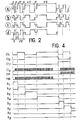
- Fig. 2 illustrates the control method of the invention. This figure represents the shape of the signals applied to the line x i and the column y j to sensitize the area x i y j of the material.
- a first series of signals a is applied to line x i divided into n different time fractions such that the k th time fraction is equal to 2 k-1 ⁇ , where k is an integer such that 1 ⁇ k ⁇ n and ⁇ a useful time interval from the excitation to the material and, on column y j , a second series of signals b or c also divided into n time fractions such that the k th time fraction of the second series of sinaux be the same duration as the fraction k iè me time the first set of corresponding signals.
- the non-selected lines are brought to the same potential which remains identical during the n time fractions of the addressing period of the line x i (first series of signals a).
- column y i receives, during the corresponding fraction of time, either a signal b of the same phase as that which is applied to line x, or a signal c in phase opposition with respect to that which is applied to said line.
- Each fraction of useful time is followed by a dead time ⁇ during which no signal is applied to the columns. During this dead time, it is possible to switch the signal b or c on the column y j so that the k th time fraction of the said signal is in phase or in phase opposition with the corresponding signal a, according to the optical characteristic of the material you want to see displayed on the imager.
- the display corresponding to the zone x i y j results from the accumulation of all the successive excitations, applied during each fraction of time on the column y j , and this throughout the addressing period of the line x i .
- the decay time of the optical effect produced by the excitation of a line is large enough for the whole image to be displayed at the end of a scan of all lines.
- the q zones of said line are simultaneously controlled by simultaneously applying to each column the signal which corresponds to it.
- the phenomenon used is the collective orientation of the molecules of said crystal parallel to the electrodes, when said crystal is subjected to an electric field.
- the phenomenon used in such an imager is described in French patent No. 2279123, previously cited.
- the excitation signal must be at zero mean value and of frequency greater than a frequency of relaxation of the charges in the liquid.
- the signals applied to the electrodes therefore have, for example, a rectangular shape (fig. 2).
- each gray level that we want to see displayed on the imager is binary coded.
- the binary element of weight 1 denoted d 1 known by the English name of bit, is used during the first fraction of time, the binary element of weight 2 denoted d 2 during the second fraction of time ..., the binary element of weight 2 n-1 noted d n during the n th fraction of time.
- the excitation of the material is obtained when the signals applied to the line x i and the column y j , for a given fraction of time are in phase opposition; this state is represented by the binary element 1.
- this state is represented by the binary element 0.
- the signal d applied to a column and corresponding to gray level 7, binary coded 0111 has been shown.
- the signal applied to the column and corresponding to bits d 1 , d 2 and d 3 is in phase opposition with the signal of the corresponding line, taken as a reference, while the signal applied to the column and corresponding to bit d 4 is in phase with the signal of said line.
- Fig. 3 schematically represents a part of the control circuits of a matrix imager according to the invention.
- said circuits make it possible to control 32 columns of electrodes of a matrix imager of the liquid crystal type with 16 gray levels.
- the means for sequentially exciting the p lines may consist of an oscillator delivering the reference signal controlled by a clock defining the application sequences of said signal.
- the control circuits of the 32 columns of the matrix imager consist of a first set of four shift registers 21, 22, 23,24 and a second set of four shift registers 25, 26, 27, 28.
- the fact of using two sets of registers makes it possible to read one of the sets of registers while the other is written, which makes it possible to increase the speed of information processing and therefore of the display on the matrix imager .
- Each of these eight registers includes a serial input, referenced D, through which the information corresponding to the four bits d 1 , d 2 , d 3 , d 4 arrives, bit d, being connected to the input D of registers 21 and 25 , bit d 2 at input D of registers 22 and 26, etc., as well as a so-called clock input referenced C1 and a high impedance control input HI.
- the eight registers 21, 22, ..., 28 also include 32 parallel outputs Sj, referenced Sj 1 for register 21, Sj 2 for register 22, ..., with j varying from 1 to 32, each connected to a 30 / d circuit (i.e. 30/1, ..., 30/32).
- Each circuit 30 / j comprises an inverter 34 and two transmission doors 36, 38 with analog signal.
- Doors 36 and 38 respectively include a control input 36/1 and 38/1 used to put the doors in the on position (door 36) or in a non-passing position (door 38), an analog signal input (b or c) 36/2 and 38/2 and a signal output 36/3 and 38/3, said output signal, coming either from door 36 or from door 38, is sent to the corresponding column y j .
- the input 36/2 of the gate 36 is connected to the output of the inverter 34, itself being connected to the input of the circuit 30 / j.
- the matrix imager control circuit further comprises a first AND gate 40 with two inputs, one receiving a clock signal C1 0 and the other a clock signal C1 T and an output delivering a HA signal applied to the inputs C1 of the first set of registers (12, 22, 23, 24) and a second AND gate 42 with two inputs, one receiving a clock signal C1 0 and the other a clock signal C1 T , the phase of which has been inverted by means of an inverter 44, and an output delivering a signal HB applied to the inputs C1 of the second set of registers (25, 26, 27, 28).
- the control circuit further comprises a decoder 46 with three inputs, the first receiving the clock signal C1 T , the second a clock signal C1, and the third a clock signal C1 2 and having 8 outputs delivering 8 signals h ,, h 2 , h 3 , h 4 , h 5 , h e , h 7 , h 8 applied respectively to registers 21, 22, 23, 24, 25, 26, 27 and 28 and controlling the high impedance input HI of said registers.
- a decoder 46 with three inputs, the first receiving the clock signal C1 T , the second a clock signal C1, and the third a clock signal C1 2 and having 8 outputs delivering 8 signals h ,, h 2 , h 3 , h 4 , h 5 , h e , h 7 , h 8 applied respectively to registers 21, 22, 23, 24, 25, 26, 27 and 28 and controlling the high impedance input HI of said registers.
- a signal consisting of four sequences of duration 2 k-1 ⁇ + ⁇ is applied to the line x i for the kth sequence.
- the division into four sequences of said signal is obtained using the clock signals C1 1 and C1 2 .
- each gray level is binary coded on four bits d ,, d 2 , d 3 and d 4 .
- the information corresponding to the different gray levels to be applied to the 32 columns of imager electrodes is entered in parallel in the four registers of the same set, each shift register being made up of 32 cells.
- the registers 21 and 25 contain the information corresponding to the least significant bit d 1 , ..., the registers 24 and 28 the information corresponding to the most significant bit d 4 .
- the sequential processing of the four bits d 1 , d2, d 3 and d 4 involves reading each set of registers sequentially, as described above.
- the selection of the register to be read is ensured by the decoder 46, that is to say that at any time seven registers among the eight have their 32 outputs set at high impedance and the eighth ensures the control of the 32 circuits 30 / j .
- the selection of the register to be read is determined by the clock signals C1 1 , C1 2 and C1 T controlling the decoder 46.
- the signal C1 T determines the set of registers to be read, C1 1 and C1 2 the register among the four of said game to read (the first sequence in the table above corresponding to the selection of register 21 or 25).
- the signals h 1 , h 2 , ..., h 8 from the decoder 46 correspond to the control of one of the eight registers.
- the reading of one of the registers of the first set takes place when the level of the signal C1 T is zero
- the reading of one of the registers of the second set takes place when the level of the signal C1 T is non-zero.
- the signal HA supplied to the first set of registers, is constituted by the superposition of two clock signals by means of the AND gate 40, one being the clock signal C1 0 , the other the clock signal C1 T.
- the clock signal HB supplied to the second set of registers, is constituted by the superposition of two clock signals by means of the AND gate 42, one being the clock signal C1 0 , l ' other the clock signal C1 T whose phase has been reversed by means of the inverter 44.
- Each clock signal HA and HB controls the collective shift, in the 32 cells, of the registers corresponding to said signals of the 32 information contained in them.
- the clock signal C1 0 comprises, for the entire duration of addressing the rows and columns of electrodes of the imager as many pulses as the registers comprise cells, therefore outputs (for example 32 pulses).
- a register set When a register set is read, it does not receive a clock signal HA and H B, while the second set, in the write position, receives the clock signal which corresponds to it.
- the first set of registers is read.
- the clock signal C1 T has a non-zero level, it is the second set of registers which is read.
- the period of the clock signal C1 T represents twice the addressing time of a line of the imager
- the level 0 of the signal C1 T corresponds to the addressing for example of even lines. of the imager, level 1 of said signal with odd lines.
Description
- La présente invention a pour objet un procédé de commande d'une caractéristique optique d'un matériau. Elletrouve une application en opto-électronique, et principalement dans la commande de cellules à cristaux liquides utilisées notamment comme convertisseurs d'informations électriques en informations optiques, dans le traitement des images optiques en temps réel, dans la réalisation de filtres colorés pouvant servir notamment en télévision en couleurs, et dans l'affichage analogique.
- Bien qu'elle s'applique à des matériaux de formes et de dimensions quelconques, l'invention concerne plus spécialement la commande d'un imageur comprenant une cellule d'affichage constituée par un matériau comprenant une pluralité de zones réparties en matrice, et intercalées dans un système dit à bandes croisées ou, en terminologie anglo-saxonne, dans un système cross-bar. De tels systèmes comprennent une première famille de p lignes d'électrodes parallèles et une deuxième famille de q colonnes d'électrodes parallèles, les lignes et les colonnes étant croisées, une zone xiyj du matériau étant définie par la région de recouvrement entre la ligne x; (où i est un entier qui peut prendre toutes les valeurs comprises entre I et p) et la colonne Yj (où j est un entier compris entre 1 et q). Les bandes formées par les lignes et les colonnes d'électrodes sont de nature telle qu'elles peuvent véhiculer des signaux appropriés à l'excitation du matériau.
- On connaît de nombreux dispositifs de ce genre qui utilisent par exemple, comme matériau sensible, un film de cristal liquide, et pour lesquels l'excitation est électrique. L'invention s'applique particulièrement bien à de tels dispositifs mais elle s'applique de manière plus générale à tout dispositif à bandes croisées comprenant un matériau dont une caractéristique optique peut être modifiée l'aide d'une excitation quelconque. Cette excitation peut être de nature électrique, comme pour les cristaux liquides, mais aussi magnétique, thermique, etc. Le matériau peut être un corps solide ou liquide, amorphe ou cristallin. La caractéristique optique peut être une opacité, un indice de réfraction, une transparence, une absorption, une diffusion, une diffraction, une convergence, un pouvoir rotatoire, une biréfrin- gence, une intensité réfléchie dans un angle solide déterminé, etc.
- En dehors des cristaux liquides, on peut citer, comme matériau utilisable, par exemple les cristaux comme le sulfure de cadmium, qui présente une bande d'absorption dont le front peut être déplacé par effet thermique. Dans ce cas, la caractéristique optique commandable est l'absorption de lumière et l'excitation est un échauffement. On peut citer aussi le cas où la caractéristique optique est l'intensité de la lumière réfléchie par une membrane déformable et où ladite excitation est une force électrostatique.
- Un procédé de commande connu consiste, par exemple, dans le cas d'une cellule à cristaux liquides où l'excitation est de nature électrique, à appliquer sur la ligne xi une tension Vx sinusoïdale et sur les autres lignes une tension nulle, et à appliquer sur les colonnes Yi des tensions Vyj sinusoïdales de même durée et de même fréquence que la tension Vx, mais qui sont déphasées par rapport à celles-ci d'une quantité ϕji. Ce déphasage ϕji permet de faire varier l'intensité du signal à afficher, c'est-à-dire permet d'obtenir différents niveaux de gris.
- Un tel procédé de commande est décrit dans le brevet français No 2279123 déposé le 6 février 1974 par le titulaire et intitulé: «Procédé de commande d'une caractéristique optique d'un matériau et imageur analogique mettant en oeuvre ledit procédé».
- Pour obtenir N niveaux de gris avec un tel procédé, il est nécessaire d'engendrer N tensions différentes Vyj. Pour appliquer sur chacune des q colonnes l'une des N tensions Vyj sans les engendrer sur chaque microplaquette de circuit intégré (appelée communément puce), il est nécessaire d'utiliser N portes de transmission par colonne, soit q fois N portes, et de réaliser N connexions par plaquette.
- La présente invention a justement pour objet un procédé de commande permettant de remédier à ces inconvénients et permettant notamment de limiter le nombre de portes de transmission et le nombre de connexion, quel que soit le nombre de niveaux de gris à afficher, c'est-à-dire de limiter la surface occupée par les connexions sur la microplaquette de circuit intégré, et ce en dépit d'une augmentation du nombre de niveaux de gris.
- D'une manière générale, l'invention concerne un procédé de commande d'une caractéristique optique d'un matériau intercalé entre deux électrodes attaquées par des signaux d'excitation, caractérisé en ce que, pour obtenir une excitation dudit matériau, on applique sur lesdites électrodes une série de signaux élémentaires pendant des durées croissantes, chaque signal élémentaire étant soit égal à une constante, soit nul, l'ensemble de ces signaux élémentaires constituant une décomposition de l'excitation désirée en une base donnée.
- De préférence, lesdites durées croissent comme des puissances de deux, l'ensemble des signaux élémentaires constituant alors une décomposition en base deux de l'excitation désirée. Mais toute autre loi de progression de durée correspondant à une autre décomposition de l'excitation est possible.
- Plus spécialement, la présente invention est un procédé de commande d'un imageur matriciel comprenant une cellule d'affichage constituée par un matériau comprenant une pluralité de zones réparties en matrice et intercalées entre une première famille de p lignes d'électrodes parallèles et une deuxième famille de q colonnes d'électrodes parallèles, les lignes et les colonnes étant croisées, une zone xiyj étant définie par la région du matériau recouvert par la ligne x;, où i est un entier tel que 1 ≤i ≤p, et par la colonne yj, où j est un entier tel que 1 ≤j ≤q, caractérisé en ce que, pour commander la zone xiyj dudit matériau, on applique sur une ligne xi une première série de signaux à valeur moyenne nulle, ladite première série étant divisée en n fractions de temps différentes, de préférence telles que la kième fraction de temps soit égale à 2k-1 T, où k est un entier tel que 1 <k ≤n et τ un intervalle de temps utile à l'excitation du matériau, et on applique sur la colonne yj une deuxième série de signaux à valeur moyenne nulle, ladite deuxième série étant également divisée en n fractions de temps telles que la kiéme fraction de temps de la deuxième série de signaux soit de même durée que la kième fraction de temps de la première série de signaux correspondante, ladite deuxième série de signaux étant telle que, pendant chaque fraction de temps, le signal de la deuxième série est soit en opposition de phase, soit en phase avec le signal de la première série correspondant.
- Le découpage temporel selon l'invention permet d'afficher N niveaux de gris en utilisant que deux déphasages entre les lignes et les colonnes alors que, dans l'art antérieur, l'affichage de N niveaux de gris nécessitait l'emploi de N déphasages. Selon un mode préféré du procédé de commande, chaque fraction de temps utile est suivie d'un temps mort µ pendant lequel aucun signal n'est appliqué aux colonnes.
- Selon un autre mode préféré du procédé de commande, on commande simultanément les q zones d'une même ligne xi en appliquant simultanément sur chaque colonne le signal de la deuxième série de signaux qui lui correspond.
- D'autres caractéristiques et avantages de l'invention ressortiront mieux de la description qui va suivre, donnée à titre purement illustratif et nullement limitatif. Pour plus de clarté, la description se réfère à la commande d'une caratéristique optique d'un cristal liquide sous l'effet d'un champ électrique appliqué. Comme on l'a indiqué plus haut, l'invention est d'application beaucoup plus générale mais, ces dispositifs à cristaux liquides étant actuellement bien connus et largement utilisés, il est préférable d'effectuer la description sur cet exemple.
- La description se réfère aux dessins annexés, dans lesquels:
- la fig. 1 représente une vue éclatée en perspective d'une cellule à cristal liquide utilisant des électrodes à bandes croisées,
- la fig. 2 représente la forme des signaux appliqués aux électrodes d'une cellule à bandes croisées,
- la fig. 3 représente schématiquement une partie des circuits de commande d'un imageur matriciel, selon l'invention,
- la fig. 4 représente schématiquement les signaux d'entrée et sortie appliqués sur les circuits de la fig. 3.
- La fig. 1 représente une cellule d'affichage à bandes croisées. Elle compte deux parois 10 et 12, généralement transparentes, disposées de part et d'autre d'une cale d'épaisseur 14, en matériau isolant, définissant un volume 16 qui est occupé, lorsque la cellule est montée, par le matériau dont on commande une caractéristique optique, par exemple un film de cristal liquide. Sur les parois 10 et 12 sont déposés deux systèmes d'électrodes constitués chacun par une série de bandes parallèles conductrices semi-transparentes, notées xi pour les lignes et y pour les colonnes. La surface utile du cristal liquide est ainsi décomposée en une mosaïque de zones correspondant aux zones de recouvrement des deux systèmes d'électrodes, chaque zone correspondant au recouvrement de deux bandes xi et yj, et qui peut, de ce fait, être repéré par la notation xiyj.
- La sensibilisation d'une zone, c'est-à-dire la commande d'une caractéristique optique du cristal liquide contenu dans cette zone, s'effectue en appliquant sur les électrodes xi et yj des tensions électriques qui entraînent l'apparition d'un champ électrique au sein du cristal liquide. On fait ainsi apparaître une image sur l'ensemble de la cellule en la définissant point par point et en sensibilisant les zones les unes après les autres selon des principes connus de commande séquentielle.
- La fig. 2 illustre le procédé de commande de l'invention. Cette figure représente la forme des signaux appliqués sur la ligne xi et la colonne yj pour sensibiliser la zone xiyj du matériau.
- Pour sensibiliser ladite zone xiyj, on applique, sur la ligne xi, une première série de signaux a divisée en n fractions de temps différentes telles que la kième fraction de temps soit égale à 2k-1 τ, où k est un entier tel que 1 ≤k ≤n et τ un intervalle de temps utile de l'excitation au matériau et, sur la colonne yj, une deuxième série de signaux b ou c également divisée en n fractions de temps telles que la kième fraction de temps de la deuxième série de sinaux soit de même durée que la kième fraction de temps de la première série de signaux correspondante.
- Les lignes non sélectionnées sont portées à un même potentiel qui reste identique pendant les n fractions de temps de la période d'adressage de la ligne xi (première série de signaux a).
- Pour chaque fraction de temps de la période d'adressage de la ligne xi, la colonne yi reçoit, pendant la fraction de temps correspondante, soit un signal b de même phase que celui qui est appliqué à la ligne x, soit un signal c en opposition de phase par rapport à celui qui est appliqué sur ladite ligne. Chaque fraction de temps utile est suivie d'un temps mort µ pendant lequel aucun signal n'est appliqué aux colonnes. Pendant ce temps mort, on peut effectuer une commutation du signal b ou c sur la colonne yj de façon que la kième fraction de temps dudit signal soit en phase ou en opposition de phase avec le signal a correspondant, suivant la caractéristique optique du matériau que l'on désire voir afficher sur l'imageur.
- L'affichage correspondant à la zone xiyj résulte de l'accumulation de toutes les excitationssucces- sives, appliquées pendant chaque fraction de temps sur la colonne yj, et ce pendant toute la période d'adressage de la ligne xi.
- Le temps de décroissance de l'effet optique produit par l'excitation d'une ligne est suffisamment grand pour que l'ensemble de l'image soit affiché à la fin d'un balayage de toutes les lignes. Pour obtenir l'affichage de toute une ligne xi de l'imageur matricial, on commande simultanément les q zones de ladite ligne en appliquant simultanément sur chaque colonne le signal qui lui correspond.
- Dans un imageur utilisant une cellule à cristal liquide, par exemple du type nématique, le phénomène utilisé est l'orientation collective des molécules dudit cristal parallèlement aux électrodes, lorsque ledit cristal est soumis à un champ électrique. Le phénomène utilisé dans un tel imageur est décrit dans le brevet français No 2279123, précédemment cité.
- Pour éviter toute perturbation dans le liquide, due notamment à des transits d'ions, le signal d'excitation doit être à valeur moyenne nulle et de fréquence supérieure à une fréquence de relaxation des charges dans le liquide. Les signaux appliqués sur les électrodes présentent donc, par exemple, une forme rectangulaire (fig. 2).
- Pour obtenir l'un des 2n niveaux de gris, on exploite successivement les n fractions de temps de la deuxième série de signaux. Chaque niveau de gris que l'on désire voir afficher sur l'imageur est codé en binaire. L'élément binaire de poids 1 noté d1, connu sous le nom anglo-saxon de bit, est exploité pendant la première fraction de temps, l'élément binaire de poids 2 noté d2 pendant la deuxième fraction de temps..., l'élément binaire de poids 2n-1 noté dn pendant la nième fraction de temps.
- L'excitation du matériau, notamment du film à cristal liquide, est obtenue lorsque les signaux appliqués sur la ligne xi et la colonne yj, pendant une fraction de temps donnée sont en opposition de phase; cet état est représenté par l'élément binaire 1. En revanche lorsque les signaux appliqués sur ladite ligne et ladite colonne, pendant ladite fraction de temps, sont en phase, il n'y a pas d'excitation du matériau; cet état est représenté par l'élément binaire 0.
- Sur la fig. 2, on a représenté le signal d appliqué sur une colonne et correspondant au niveau de gris 7, codé en binaire 0111. Le signal appliqué sur la colonne et correspondant aux bits d1, d2 et d3 est en opposition de phase avec le signal de la ligne correspondante, pris comme référence, tandis que le signal appliqué sur la colonne et correspondant au bit d4 est en phase avec le signal de ladite ligne.
- La fig. 3 représente schématiquement une partie des circuits de commande d'un imageur matriciel selon l'invention. Dans le mode de réalisation représenté sur cette figure, lesdits circuits permettent de commander 32 colonnes d'électrodes d'un imageur matriciel du type à cristaux liquides avec 16 niveaux de gris. Les moyens d'excitation séquentielle des p lignes, non représentés sur cette figure, peuvent être constitués d'un oscillateur délivrant le signal de référence commandé par une horloge définissant les séquences d'application dudit signal.
- Les circuits de commande des 32 colonnes de l'imageur matriciel sont constitués d'un premier jeu de quatre registres à décalage 21, 22, 23,24 et d'un deuxième jeu de quatre registres à décalage 25, 26, 27, 28. Le fait d'utiliser deux jeux de registres permet de lire l'un des jeux de registres pendant que l'autre est écrit, ce qui permet d'augmenter la vitesse de traitement des informations et donc de l'affichage sur l'imageur matriciel. Chacun de ces huit registres comprend une entrée série, référencée D, par laquelle arrivent les informations correspondant aux quatres bits d1, d2, d3, d4, le bit d, étant relié à l'entrée D des registres 21 et 25, le bit d2 à l'entrée D des registres 22 et 26, etc., ainsi qu'une entrée dite d'horloge référencée C1 et une entrée de commande HI à haute impédance.
- Les huit registres 21, 22, ..., 28 comprennent de plus 32 sorties parallèles Sj, référencées Sj1 pour le registre 21, Sj2 pour le registre 22, ..., avec j variant de 1 à 32, reliées chacune à un circuit 30/j (soit 30/1, ..., 30/32). Chaque circuit 30/j comporte un inverseur 34 et deux portes de transmission 36, 38 à signal analogique.
- Les portes 36 et 38 comprennent respectivement une entrée de commande 36/1 et 38/1 servant à mettre les portes en position passante (porte 36) ou en position non passante (porte 38), une entrée de signal analogique (b ou c) 36/2 et 38/2 et une sortie de signal 36/3 et 38/3, ledit signal de sortie, issu soit de la porte 36, soit de la porte 38, est envoyé sur la colonne yj correspondante. L'entrée 36/2 de la porte 36 est connectée à la sortie de l'inverseur 34, lui-même étant connecté à l'entrée du circuit 30/j.
- Le circuit de commande de l'imageur matriciel comprend, de plus, une première porte ET 40 à deux entrées, l'une recevant un signal d'horloge C10 et l'autre un signal d'horloge C1 T et une sortie délivrant un signal HA appliqué aux entrées C1 du premier jeu de registres (12, 22, 23, 24) et une deuxième porte ET 42 à deux entrées, l'une recevant un signal d'horloge C10 et l'autre un signal d'horloge C1T, dont la phase a été inversée au moyen d'un inverseur 44, et une sortie délivrant un signal H B appliqué aux entrées C1 du deuxième jeu de registres (25, 26, 27, 28).
- Le circuit de commande comprend encore un décodeur 46 à trois entrées, la première recevant le signal d'horloge C1T, la deuxième un signal d'horloge C1, et la troisième un signal d'horloge C12 et comportant 8 sorties délivrant 8 signaux h,, h2, h3, h4, h5, he, h7, h8 appliqués respectivement aux registres 21, 22, 23, 24, 25, 26, 27 et 28 et commandant l'entrée haute impédance HI desdits registres.
- On va maintenant décrire le fonctionnement du circuit de commande en se référant à la fig. 4, sur laquelle on a représenté les différents signaux apparaissant à différents points dudit circuit:
- les signaux d'horloge C11, C12 sont envoyés sur le décodeur 46,
- le signal d'horloge C1 T est envoyé à la fois sur le décodeur 46, sur la porte 40 et sur l'inverseur 44,
- le signal d'horloge C1 0 est envoyé sur la porte 40 et sur la porte 42,
- les signaux HA et H B sortant respectivement de la porte 40 et de la porte 42 sont envoyés respectivement sur le premier et sur le deuxième jeu de registres,
- les signaux h1, h2, h3, h4, h5, h6, h7, h8 issus du décodeur 46 sont envoyés respectivement sur l'entrée haute impédance HI des registres 21, 22, 23, 24, 25, 26, 27 et 28.
- Selon l'invention, pour obtenir un niveau de gris donné sur la zone xiyj d'un imageur matriciel, on applique sur la ligne xi un signal a constitué de quatre séquences de durée 2k-1 τ+µ pour la kième séquence. Le découpage en quatre séquences dudit signal est obtenu à l'aide des signaux d'horloge C11 et C12.
- Cette découpe est assurée par le niveau respectif des signaux C11 et C12. Letableau ci-après illustre un exemple de découpage du signal de la ligne xi de l'imageur.

- Comme on l'a vu précédemment, chaque niveau de gris est codé en binaire sur quatre bits d,, d2, d3 et d4. L'entrée des informations correspondant aux différents niveaux de gris à appliquer sur les 32 colonnes d'électrodes de l'imageur se fait en parallèle dans les quatre registres d'un même jeu, chaque registre à décalage étant constitué de 32 cellules. Les registres 21 et 25 contiennent les informations correspondant au bit de poids faible d1, ..., les registres 24 et 28 les informations correspondant au bit de poids fort d4.
- L'exploitation séquentielle des quatre bits d1, d2, d3 et d4 implique une lecture de façon séquentielle de chaque jeu de registres, comme décrit précédemment. La sélection du registre à lire est assurée par le décodeur 46, c'est-à-dire qu'à tout instant sept registres parmi les huit ont leurs 32 sorties mises en haute impédance et le huitième assure la commande des 32 circuits 30/j. La sélection du registre à lire est déterminée par les signaux d'horloge C11, C12 et C1 T commandant le décodeur 46. Le signal C1T détermine le jeu de registres à lire, C11 et C12 le registre parmi les quatre dudit jeu à lire (la première séquence du tableau ci-dessus correspondant à la sélection du registre 21 ou 25). Les signaux h1, h2, ..., h8 issus du décodeur 46 correspondent à la commande d'un des huit registres. La lecture de l'un des registres du premier jeu a lieu lorsque le niveau du signal C1T est nul, la lecture de l'un des registres du deuxième jeu a lieu lorsque le niveau du signal C1 T est non nul.
- Le registre en position lecture assure la commande des 32 circuits 30/j. L'un des signaux analogues b ou c arrivant par l'entrée 36/2 ou 38/2 des portes 36 et 38 est transmis à ladite colonne suivant que les portes 36 et 38 sont en position passante ou non passante. Par exemple, lorsque la porte 36 est en position passante et que la porte 38 est en position non passante, c'est le signal b qui est transmis. Inversement, lorsque la porte 38 est en position passante et que la porte 36 est en position non passante, c'est le signal c qui est transmis. La commande des portes en position passante ou non passante, réalisée au moyen de l'inverseur 34, dépend du signal arrivant à l'entrée du circuit 30/j. Après avoir lu de cette façon les 4 registres d'un même jeu, le signal final reçu par la colonne yj est par exemple le signal d (fig. 2) correspondant à l'affichage sur l'imageur du septième niveau de gris. L'utilisation d'un registre à décalage à 32 cellules permet d'afficher simultanément sur les 32 colonnes de l'imageur le niveau de gris qui lui correspond (affichage simultané d'une ligne de l'imageur).
- Le fait d'utiliser deux jeux de registres permet de lire l'un des jeux pendant que le deuxième est écrit, c'est-à-dire que ce dernier enregistre les 32 informations de même poids (d,, d2, d3, d4) correspondant aux 32 colonnes de l'imageur.
- L'enregistrement des informations est lié aux signaux d'horloge HA et HB envoyés respectivement sur le premier jeu et le deuxième jeu de registres.
- Le signal HA, fourni au premier jeu de registres, est constitué par la superposition de deux signaux d'horloge au moyen de la porte ET 40, l'un étant le signal d'horloge C10, l'autre le signal d'horloge C1T. De même, le signal d'horloge H B, fourni au deuxième jeu de registres, est constitué par la superposition de deux signaux d'horloge au moyen de la porte ET 42, l'un étant le signal d'horloge C10, l'autre le signal d'horloge C1 T dont la phase a été inversée au moyen de l'inverseur 44.
- Chaque signal d'horloge HA et HB commande le décalage collectif, dans les 32 cellules, des registres correspondant auxdits signaux des 32 informations contenues dans ceux-ci.
- De ce fait, le signal d'horloge C10 comporte, pendant toute la durée d'adressage des lignes et des colonnes d'électrodes de l'imageur autant d'impulsions que les registres comportent de cellules, donc de sorties (par exemple 32 impulsions).
- Lorsqu'un jeu de registre est lu, il ne reçoit pas de signal d'horloge HA et H B, tandis que le deuxième jeu, en position écriture, reçoit le signal d'horloge qui lui correspond.
- Si le signal d'horloge C1T présente un niveau nul, c'est le premier jeu de registre qui est lu. En revanche, si le signal d'horloge C1T présente un niveau non nul, c'est le deuxième jeu de registre qui est lu.
- Il est à noter que la période du signal d'horloge C1T représente le double d'un temps d'adressage d'une ligne de l'imageur, le niveau 0 du signal C1T correspond à l'adressage par exemple des lignes paires de l'imageur, le niveau 1 dudit signal aux lignes impaires.
- Le fait d'appliquer après chaque fraction de temps un temps mort µ permet de commuter les différents signaux à appliquer sur les colonnes de l'imageur et, en particulier, permet la commutation ou non des portes 36 et 38 en préservant de la déformation le signal de commande desdites colonnes, déformation induite par la commutation desdites portes. Cela permet en outre d'éviter l'existence d'une composante continue.
Claims (6)
Applications Claiming Priority (2)
| Application Number | Priority Date | Filing Date | Title |
|---|---|---|---|
| FR8022930A FR2493012B1 (fr) | 1980-10-27 | 1980-10-27 | Procede de commande d'une caracteristique optique d'un materiau |
| FR8022930 | 1980-10-27 |
Publications (2)
| Publication Number | Publication Date |
|---|---|
| EP0051521A1 EP0051521A1 (fr) | 1982-05-12 |
| EP0051521B1 true EP0051521B1 (fr) | 1984-08-22 |
Family
ID=9247345
Family Applications (1)
| Application Number | Title | Priority Date | Filing Date |
|---|---|---|---|
| EP81401664A Expired EP0051521B1 (fr) | 1980-10-27 | 1981-10-21 | Procédé de commande d'une caractéristique optique d'un matériau |
Country Status (6)
| Country | Link |
|---|---|
| US (1) | US4427979A (fr) |
| EP (1) | EP0051521B1 (fr) |
| JP (1) | JPS57109995A (fr) |
| CA (1) | CA1198534A (fr) |
| DE (1) | DE3165704D1 (fr) |
| FR (1) | FR2493012B1 (fr) |
Families Citing this family (36)
| Publication number | Priority date | Publication date | Assignee | Title |
|---|---|---|---|---|
| DE3142906A1 (de) * | 1981-10-29 | 1983-05-11 | Fa. Carl Zeiss, 7920 Heidenheim | Stufenweise ladungssteuerung fuer elektrochrome schichten |
| US4525710A (en) * | 1982-02-16 | 1985-06-25 | Seiko Instruments & Electronics Ltd. | Picture display device |
| CH666560A5 (de) * | 1983-03-01 | 1988-07-29 | Tadeusz Bobak | Anzeigevorrichtung. |
| US4651148A (en) * | 1983-09-08 | 1987-03-17 | Sharp Kabushiki Kaisha | Liquid crystal display driving with switching transistors |
| JPS6083477A (ja) * | 1983-10-13 | 1985-05-11 | Sharp Corp | 液昇表示装置の駆動回路 |
| GB2161637B (en) * | 1984-07-12 | 1988-01-13 | Stc Plc | Addressing smectic displays |
| US4709995A (en) * | 1984-08-18 | 1987-12-01 | Canon Kabushiki Kaisha | Ferroelectric display panel and driving method therefor to achieve gray scale |
| FR2580110B1 (fr) * | 1985-04-04 | 1987-05-29 | Commissariat Energie Atomique | |
| US4707078A (en) * | 1985-04-26 | 1987-11-17 | American Telephone And Telegraph Company, At&T Bell Laboratories | Ferroelectric liquid crystal devices using field-stabilized states |
| USRE38661E1 (en) * | 1986-01-13 | 2004-11-30 | Hitachi, Ltd. | Method and apparatus for liquid crystal display with intermediate tone |
| JPH0827601B2 (ja) * | 1986-01-13 | 1996-03-21 | 株式会社日立製作所 | 液晶表示装置、及びその駆動方法 |
| FR2594579B1 (fr) * | 1986-02-17 | 1988-04-15 | Commissariat Energie Atomique | Ecran d'affichage a matrice active permettant l'affichage de niveaux de gris |
| US4750813A (en) * | 1986-02-28 | 1988-06-14 | Hitachi, Ltd. | Display device comprising a delaying circuit to retard signal voltage application to part of signal electrodes |
| GB8622715D0 (en) * | 1986-09-20 | 1986-10-29 | Emi Plc Thorn | Display device |
| US5189406A (en) * | 1986-09-20 | 1993-02-23 | Thorn Emi Plc | Display device |
| FR2605444A1 (fr) * | 1986-10-17 | 1988-04-22 | Thomson Csf | Procede de commande d'un ecran matriciel electrooptique et circuit de commande mettant en oeuvre ce procede |
| US5157386A (en) * | 1987-06-04 | 1992-10-20 | Seiko Epson Corporation | Circuit for driving a liquid crystal display panel |
| JPH0750389B2 (ja) * | 1987-06-04 | 1995-05-31 | セイコーエプソン株式会社 | 液晶パネルの駆動回路 |
| US4833464A (en) * | 1987-09-14 | 1989-05-23 | Copytele, Inc. | Electrophoretic information display (EPID) apparatus employing grey scale capability |
| FR2633764B1 (fr) * | 1988-06-29 | 1991-02-15 | Commissariat Energie Atomique | Procede et dispositif de commande d'un ecran matriciel affichant des niveaux de gris |
| KR900702501A (ko) * | 1988-09-16 | 1990-12-07 | 원본미기재 | 평판 그래픽 디스플레이를 위한 그레이 스케일 방법 및 회로 |
| US5196839A (en) * | 1988-09-16 | 1993-03-23 | Chips And Technologies, Inc. | Gray scales method and circuitry for flat panel graphics display |
| JP2619028B2 (ja) * | 1988-11-30 | 1997-06-11 | シャープ株式会社 | 表示装置の駆動方法および装置 |
| US5298915A (en) * | 1989-04-10 | 1994-03-29 | Cirrus Logic, Inc. | System and method for producing a palette of many colors on a display screen having digitally-commanded pixels |
| US5185602A (en) * | 1989-04-10 | 1993-02-09 | Cirrus Logic, Inc. | Method and apparatus for producing perception of high quality grayscale shading on digitally commanded displays |
| JPH03132692A (ja) * | 1989-10-18 | 1991-06-06 | Matsushita Electric Ind Co Ltd | 液晶表示装置の駆動方法及びその駆動回路 |
| JP2794499B2 (ja) | 1991-03-26 | 1998-09-03 | 株式会社半導体エネルギー研究所 | 半導体装置の作製方法 |
| US5414442A (en) * | 1991-06-14 | 1995-05-09 | Semiconductor Energy Laboratory Co., Ltd. | Electro-optical device and method of driving the same |
| US6975296B1 (en) | 1991-06-14 | 2005-12-13 | Semiconductor Energy Laboratory Co., Ltd. | Electro-optical device and method of driving the same |
| US6778231B1 (en) | 1991-06-14 | 2004-08-17 | Semiconductor Energy Laboratory Co., Ltd. | Electro-optical display device |
| JP3349527B2 (ja) | 1991-10-01 | 2002-11-25 | 株式会社日立製作所 | 液晶中間調表示装置 |
| JP2639763B2 (ja) * | 1991-10-08 | 1997-08-13 | 株式会社半導体エネルギー研究所 | 電気光学装置およびその表示方法 |
| US5751265A (en) * | 1991-12-24 | 1998-05-12 | Cirrus Logic, Inc. | Apparatus and method for producing shaded images on display screens |
| WO1993013513A1 (fr) * | 1991-12-24 | 1993-07-08 | Cirrus Logic, Inc. | Procede de production d'images ombrees sur des ecrans d'affichage |
| US7164405B1 (en) * | 1998-06-27 | 2007-01-16 | Lg.Philips Lcd Co., Ltd. | Method of driving liquid crystal panel and apparatus |
| US8355015B2 (en) | 2004-05-21 | 2013-01-15 | Semiconductor Energy Laboratory Co., Ltd. | Semiconductor device, display device and electronic device including a diode electrically connected to a signal line |
Family Cites Families (10)
| Publication number | Priority date | Publication date | Assignee | Title |
|---|---|---|---|---|
| CA949159A (en) * | 1970-06-20 | 1974-06-11 | Teruo Sato | Scanning apparatus for dc el crossed-grid panel |
| JPS5757718B2 (fr) * | 1973-10-19 | 1982-12-06 | Hitachi Ltd | |
| US4006298A (en) | 1975-05-20 | 1977-02-01 | Gte Laboratories Incorporated | Bistable matrix television display system |
| FR2327603A1 (fr) * | 1975-10-06 | 1977-05-06 | Telediffusion Fse | Systeme electro-optique de visualisation et, eventuellement, d'enregistrement photographique |
| NL7603056A (nl) * | 1976-03-24 | 1977-09-27 | Philips Nv | Televisieweergeefinrichting. |
| JPS5397A (en) * | 1976-06-24 | 1978-01-05 | Hitachi Ltd | Luminance control signal formation method for gradation display |
| JPS53105317A (en) | 1977-02-25 | 1978-09-13 | Hitachi Ltd | Luminance adjusting circuit |
| US4180813A (en) | 1977-07-26 | 1979-12-25 | Hitachi, Ltd. | Liquid crystal display device using signal converter of digital type |
| DE2938759A1 (de) * | 1979-09-25 | 1981-03-26 | Siemens AG, 1000 Berlin und 8000 München | Verfahren zum ansteuern einer gasentladungsanzeigevorrichtung |
| US4319239A (en) | 1980-05-27 | 1982-03-09 | Hughes Aircraft Company | CCD Capacitance modulation matrix for liquid crystal displays |
-
1980
- 1980-10-27 FR FR8022930A patent/FR2493012B1/fr not_active Expired
-
1981
- 1981-10-16 CA CA000388149A patent/CA1198534A/fr not_active Expired
- 1981-10-20 US US06/313,156 patent/US4427979A/en not_active Expired - Fee Related
- 1981-10-21 DE DE8181401664T patent/DE3165704D1/de not_active Expired
- 1981-10-21 EP EP81401664A patent/EP0051521B1/fr not_active Expired
- 1981-10-27 JP JP56171988A patent/JPS57109995A/ja active Pending
Also Published As
| Publication number | Publication date |
|---|---|
| FR2493012A1 (fr) | 1982-04-30 |
| FR2493012B1 (fr) | 1987-04-17 |
| US4427979A (en) | 1984-01-24 |
| EP0051521A1 (fr) | 1982-05-12 |
| CA1198534A (fr) | 1985-12-24 |
| JPS57109995A (en) | 1982-07-08 |
| DE3165704D1 (en) | 1984-09-27 |
Similar Documents
| Publication | Publication Date | Title |
|---|---|---|
| EP0051521B1 (fr) | Procédé de commande d'une caractéristique optique d'un matériau | |
| EP0055966B1 (fr) | Dispositif d'affichage matriciel comprenant deux familles d'électrodes lignes et son procédé de commande | |
| EP0058593B1 (fr) | Dispositif d'affichage matriciel à plusieurs jeux d'électrodes et son procédé de commande | |
| EP0201369B1 (fr) | Procédé de commande d'un dispositif d'affichage matriciel affichant des niveaux de gris | |
| FR2569294A1 (fr) | Panneau d'affichage et son procede de commande | |
| FR2542119A1 (fr) | Procede pour commander un ecran d'affichage matriciel a cristaux liquides | |
| FR2530852A1 (fr) | Dispositif d'affichage d'images a cristal liquide | |
| EP2721598B1 (fr) | Afficheur a cristal liquide a electrodes d'effacement | |
| EP0123568B1 (fr) | Imageur matriciel à dispositif de compensation du couplage entre les lignes et les colonnes | |
| EP0120732B1 (fr) | Procédé de commande séquentielle d'un imageur matriciel utilisant l'effet de transition de phase cholestérique-nématique d'un cristal liquide | |
| FR2578670A1 (fr) | Dispositif et procede de modulation optique | |
| EP0105767B1 (fr) | Procédé de commande d'un imageur matriciel | |
| FR2580826A1 (fr) | Procede et appareil de commande d'un dispositif de modulation optique | |
| EP0237539B1 (fr) | Dispositif de commande d'un imageur matriciel a memoire integree et son procede de commande | |
| CH621204A5 (fr) | ||
| EP0817378B1 (fr) | Générateur d'impulsions électroniques programmables en durée et en fréquence | |
| FR2551245A1 (fr) | Procede et dispositif pour l'affichage de symboles a l'aide d'une matrice a cristaux liquides | |
| EP0692780A1 (fr) | Dispositif de visualisation à cristaux liquides, à matrice active et à contre-électrode fractionnee | |
| EP0176384B1 (fr) | Ecran matriciel polychrome sans couplage entre les lignes et les colonnes | |
| EP2104094A1 (fr) | Dispositif d'affichage pouvant fonctionner en mode partiel d'affichage basse consommation | |
| WO1992011560A1 (fr) | Ecran electrooptique matriciel a commande active a systeme de test integre | |
| FR2473767A1 (fr) | Circuit de commande des phases de plusieurs potentiels electriques alternatifs de meme frequence, notamment pour matrice d'affichage a cristaux liquides | |
| FR2578671A1 (fr) | Circuit de commande d'un panneau a plasma de type alternatif | |
| EP0057805A2 (fr) | Dispositif d'affichage électro-optique à matrice de points | |
| FR2520885A1 (fr) | Dispositif de transfert d'information dans un milieu optique non lineaire |
Legal Events
| Date | Code | Title | Description |
|---|---|---|---|
| PUAI | Public reference made under article 153(3) epc to a published international application that has entered the european phase |
Free format text: ORIGINAL CODE: 0009012 |
|
| AK | Designated contracting states |
Designated state(s): CH DE GB IT NL |
|
| 17P | Request for examination filed |
Effective date: 19821008 |
|
| ITF | It: translation for a ep patent filed |
Owner name: JACOBACCI & PERANI S.P.A. |
|
| GRAA | (expected) grant |
Free format text: ORIGINAL CODE: 0009210 |
|
| AK | Designated contracting states |
Designated state(s): CH DE GB IT LI NL |
|
| REF | Corresponds to: |
Ref document number: 3165704 Country of ref document: DE Date of ref document: 19840927 |
|
| PLBE | No opposition filed within time limit |
Free format text: ORIGINAL CODE: 0009261 |
|
| STAA | Information on the status of an ep patent application or granted ep patent |
Free format text: STATUS: NO OPPOSITION FILED WITHIN TIME LIMIT |
|
| 26N | No opposition filed | ||
| PGFP | Annual fee paid to national office [announced via postgrant information from national office to epo] |
Ref country code: DE Payment date: 19890925 Year of fee payment: 9 |
|
| PGFP | Annual fee paid to national office [announced via postgrant information from national office to epo] |
Ref country code: GB Payment date: 19890930 Year of fee payment: 9 |
|
| PGFP | Annual fee paid to national office [announced via postgrant information from national office to epo] |
Ref country code: CH Payment date: 19891018 Year of fee payment: 9 |
|
| ITTA | It: last paid annual fee | ||
| PGFP | Annual fee paid to national office [announced via postgrant information from national office to epo] |
Ref country code: NL Payment date: 19891031 Year of fee payment: 9 |
|
| PG25 | Lapsed in a contracting state [announced via postgrant information from national office to epo] |
Ref country code: GB Effective date: 19901021 |
|
| PG25 | Lapsed in a contracting state [announced via postgrant information from national office to epo] |
Ref country code: LI Effective date: 19901031 Ref country code: CH Effective date: 19901031 |
|
| PG25 | Lapsed in a contracting state [announced via postgrant information from national office to epo] |
Ref country code: NL Effective date: 19910501 |
|
| NLV4 | Nl: lapsed or anulled due to non-payment of the annual fee | ||
| GBPC | Gb: european patent ceased through non-payment of renewal fee | ||
| REG | Reference to a national code |
Ref country code: CH Ref legal event code: PL |
|
| PG25 | Lapsed in a contracting state [announced via postgrant information from national office to epo] |
Ref country code: DE Effective date: 19910702 |