EP0051505B1 - Transistor émetteur-récepteur de lumière pour télécommunications à l'alternat sur fibre optique - Google Patents
Transistor émetteur-récepteur de lumière pour télécommunications à l'alternat sur fibre optique Download PDFInfo
- Publication number
- EP0051505B1 EP0051505B1 EP81401533A EP81401533A EP0051505B1 EP 0051505 B1 EP0051505 B1 EP 0051505B1 EP 81401533 A EP81401533 A EP 81401533A EP 81401533 A EP81401533 A EP 81401533A EP 0051505 B1 EP0051505 B1 EP 0051505B1
- Authority
- EP
- European Patent Office
- Prior art keywords
- layer
- substrate
- conductivity
- type
- transistor
- Prior art date
- Legal status (The legal status is an assumption and is not a legal conclusion. Google has not performed a legal analysis and makes no representation as to the accuracy of the status listed.)
- Expired
Links
- 239000013307 optical fiber Substances 0.000 title claims description 4
- 239000000758 substrate Substances 0.000 claims description 27
- 239000000203 mixture Substances 0.000 claims description 10
- 239000000463 material Substances 0.000 claims description 7
- 239000004065 semiconductor Substances 0.000 claims description 7
- 229910001218 Gallium arsenide Inorganic materials 0.000 claims 3
- 239000013078 crystal Substances 0.000 claims 2
- 230000005540 biological transmission Effects 0.000 description 4
- GPXJNWSHGFTCBW-UHFFFAOYSA-N Indium phosphide Chemical compound [In]#P GPXJNWSHGFTCBW-UHFFFAOYSA-N 0.000 description 3
- 230000003321 amplification Effects 0.000 description 3
- 238000009792 diffusion process Methods 0.000 description 3
- 239000000835 fiber Substances 0.000 description 3
- 229910052733 gallium Inorganic materials 0.000 description 3
- 229910052738 indium Inorganic materials 0.000 description 3
- 238000003199 nucleic acid amplification method Methods 0.000 description 3
- 229910052698 phosphorus Inorganic materials 0.000 description 3
- 229910052785 arsenic Inorganic materials 0.000 description 2
- 230000002349 favourable effect Effects 0.000 description 2
- 239000012535 impurity Substances 0.000 description 2
- 230000004807 localization Effects 0.000 description 2
- 230000010287 polarization Effects 0.000 description 2
- GYHNNYVSQQEPJS-UHFFFAOYSA-N Gallium Chemical compound [Ga] GYHNNYVSQQEPJS-UHFFFAOYSA-N 0.000 description 1
- OAICVXFJPJFONN-UHFFFAOYSA-N Phosphorus Chemical compound [P] OAICVXFJPJFONN-UHFFFAOYSA-N 0.000 description 1
- 238000010521 absorption reaction Methods 0.000 description 1
- 238000007796 conventional method Methods 0.000 description 1
- 238000001514 detection method Methods 0.000 description 1
- 230000000694 effects Effects 0.000 description 1
- 230000005684 electric field Effects 0.000 description 1
- 238000005530 etching Methods 0.000 description 1
- 238000002513 implantation Methods 0.000 description 1
- APFVFJFRJDLVQX-UHFFFAOYSA-N indium atom Chemical compound [In] APFVFJFRJDLVQX-UHFFFAOYSA-N 0.000 description 1
- 230000000873 masking effect Effects 0.000 description 1
- 238000001465 metallisation Methods 0.000 description 1
- 230000005693 optoelectronics Effects 0.000 description 1
- 239000011574 phosphorus Substances 0.000 description 1
- 229910002059 quaternary alloy Inorganic materials 0.000 description 1
- 238000000926 separation method Methods 0.000 description 1
Images

Classifications
-
- H—ELECTRICITY
- H10—SEMICONDUCTOR DEVICES; ELECTRIC SOLID-STATE DEVICES NOT OTHERWISE PROVIDED FOR
- H10F—INORGANIC SEMICONDUCTOR DEVICES SENSITIVE TO INFRARED RADIATION, LIGHT, ELECTROMAGNETIC RADIATION OF SHORTER WAVELENGTH OR CORPUSCULAR RADIATION
- H10F30/00—Individual radiation-sensitive semiconductor devices in which radiation controls the flow of current through the devices, e.g. photodetectors
- H10F30/20—Individual radiation-sensitive semiconductor devices in which radiation controls the flow of current through the devices, e.g. photodetectors the devices having potential barriers, e.g. phototransistors
- H10F30/21—Individual radiation-sensitive semiconductor devices in which radiation controls the flow of current through the devices, e.g. photodetectors the devices having potential barriers, e.g. phototransistors the devices being sensitive to infrared, visible or ultraviolet radiation
- H10F30/24—Individual radiation-sensitive semiconductor devices in which radiation controls the flow of current through the devices, e.g. photodetectors the devices having potential barriers, e.g. phototransistors the devices being sensitive to infrared, visible or ultraviolet radiation the devices having only two potential barriers, e.g. bipolar phototransistors
- H10F30/245—Bipolar phototransistors
-
- H—ELECTRICITY
- H10—SEMICONDUCTOR DEVICES; ELECTRIC SOLID-STATE DEVICES NOT OTHERWISE PROVIDED FOR
- H10F—INORGANIC SEMICONDUCTOR DEVICES SENSITIVE TO INFRARED RADIATION, LIGHT, ELECTROMAGNETIC RADIATION OF SHORTER WAVELENGTH OR CORPUSCULAR RADIATION
- H10F55/00—Radiation-sensitive semiconductor devices covered by groups H10F10/00, H10F19/00 or H10F30/00 being structurally associated with electric light sources and electrically or optically coupled thereto
- H10F55/18—Radiation-sensitive semiconductor devices covered by groups H10F10/00, H10F19/00 or H10F30/00 being structurally associated with electric light sources and electrically or optically coupled thereto wherein the radiation-sensitive semiconductor devices and the electric light source share a common body having dual-functionality of light emission and light detection
-
- H—ELECTRICITY
- H10—SEMICONDUCTOR DEVICES; ELECTRIC SOLID-STATE DEVICES NOT OTHERWISE PROVIDED FOR
- H10H—INORGANIC LIGHT-EMITTING SEMICONDUCTOR DEVICES HAVING POTENTIAL BARRIERS
- H10H20/00—Individual inorganic light-emitting semiconductor devices having potential barriers, e.g. light-emitting diodes [LED]
- H10H20/80—Constructional details
- H10H20/81—Bodies
- H10H20/813—Bodies having a plurality of light-emitting regions, e.g. multi-junction LEDs or light-emitting devices having photoluminescent regions within the bodies
Definitions
- the invention relates to optoelectronic components capable of operating alternately as a transmitter and as a receiver, and of being coupled under conditions favorable to an optical fiber, in particular to those of the type used in telecommunications.
- the components used hitherto include diodes with double hetero-structure, operating in light-emitting diodes under direct polarization of the semiconductor junction, and in photodiodes, optionally with amplification gain, under reverse polarization.
- diodes with double hetero-structure operating in light-emitting diodes under direct polarization of the semiconductor junction, and in photodiodes, optionally with amplification gain, under reverse polarization.
- Such a diode is, for example, described in FR-A-2 387 519.
- the invention seeks to remedy these drawbacks by using a heterostructure comprising a phototransistor.
- the transistor according to the invention is of the type comprising a semiconductor substrate and a series of semiconductor layers comprising at least one active layer located between two heterojunctions as claimed in claim 1.
- the substrate can be of the n or p type, and the phototransistor of the npn or pnp type.
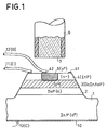
- Figures 1 and 2 are described for an npn transistor in the quaternary system.
- a substrate 1 is shown, made of n + doped indium phosphide (concentration greater than or equal to 10 17 cm -3 ).
- Semiconductor layers 2, 3 and 4 were deposited on this substrate and a mesa etching of circular shape was carried out on the assembly up to the substrate 1, inclusive.
- Layer 2 is made of n-doped indium phosphide with a lower concentration than that of the substrate is from 10 15 to 10 16 cm -3 . Its thickness can vary from 2 (maximum doping case) to 20 microns (minimum doping case). This thickness is calculated as a function of the concentration and of the supply voltages capable of creating electric fields capable of putting the entire layer in the space charge regime.
- the p + doping is of the order of 10 18 cm -3 .
- the thickness is 1 to 2 microns.
- Layer 4 is made of n- type InP (concentration of 10 16 cm- 3 ) with a thickness of 1 to 3 microns.
- a region 5 is produced, substantially cylindrical and placed at the center of the circular mesa structure. It presents a strong p + doping (concentration greater than 10 17 cm -3 ) by the use of a conventional method of implantation or localized diffusion of p-type impurities. In particular, in the case of diffusion, masking is necessary to prevent the diffusion of impurities outside the chosen region (5).
- ohmic contacts 41 and 42 are made.
- the contact 41 is annular and located at the periphery of the free surface of the layer 4.
- the contact 42 is made on the surface of the region 5.
- Connections 11 (E) and 12 (B) are soldered to contacts 41 and 42, respectively, to serve as transmitter and base connections.
- a collector connection 13 (C) is welded to a metallization 10 previously produced on the face of the substrate opposite layers 1 to 4.
- an optical fiber 6 whose core has a planar face 7.
- the surface of region 5 should preferably be less than that of the plane entry face of the fiber, so that the light emission coming from layer 3, in the region below region 5, penetrates essentially into the heart of the fiber. Under these conditions, the operation on transmission is favorable to good transmission, and, as regards reception conditions, it is desirable that the surface of region 5 is of the same order as the entry face of the fiber. .
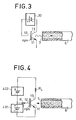
- FIG 4 there is shown a different connection mode from that of Figure 3 and which corresponds to the cause of the phototransistor operation.
- a DC voltage source 401 is connected by its pole - to the emitter 11 and by its + pole to the base 12 through a resistor R.
- a DC voltage source 402 is connected by its pole - to the + pole of the source 401 and by its pole + to the collector 13 through a receiver R L.
- the photons absorbed in layer 3 give rise to pairs of electrons and holes which generate the primary current. This current is amplified by transistor effect and gives rise to a collector current which crosses the receiver R L which plays the role of photonic current detector.
- FIG. 2 represents a variant of the embodiment of FIG. 1.
- the same references designate the same elements.
- the semiconductor structure of this variant differs from the previous one by the presence of an additional layer 20 and by a different thickness from layer 3, here much thinner (0.2 to 0.5 microns).
- the doping has a concentration of atoms n - from 10 15 to 10 16 cm -3 .
- Layer 2 is of the same nature and of the same doping as in the structure of FIG. 1.
- the rest of the device is the same for the two embodiments.
- the operation is analogous and the circuits of use identical. The only difference comes from the separation of the photonic emission and detection layers, in the second embodiment.
- the invention applies to transistors of the reverse type, ie pnp, instead of the npn type of the above description, provided that the polarities of the voltages applied to the devices are changed.
Landscapes
- Led Devices (AREA)
- Light Receiving Elements (AREA)
- Led Device Packages (AREA)
Applications Claiming Priority (2)
| Application Number | Priority Date | Filing Date | Title |
|---|---|---|---|
| FR8023015A FR2493047A1 (fr) | 1980-10-28 | 1980-10-28 | Transistor emetteur-recepteur de lumiere pour telecommunications a l'alternat sur fibre optique |
| FR8023015 | 1980-10-28 |
Publications (2)
| Publication Number | Publication Date |
|---|---|
| EP0051505A1 EP0051505A1 (fr) | 1982-05-12 |
| EP0051505B1 true EP0051505B1 (fr) | 1983-04-13 |
Family
ID=9247398
Family Applications (1)
| Application Number | Title | Priority Date | Filing Date |
|---|---|---|---|
| EP81401533A Expired EP0051505B1 (fr) | 1980-10-28 | 1981-10-02 | Transistor émetteur-récepteur de lumière pour télécommunications à l'alternat sur fibre optique |
Country Status (5)
| Country | Link |
|---|---|
| US (1) | US4485391A (enExample) |
| EP (1) | EP0051505B1 (enExample) |
| JP (1) | JPS57102082A (enExample) |
| DE (1) | DE3160184D1 (enExample) |
| FR (1) | FR2493047A1 (enExample) |
Families Citing this family (27)
| Publication number | Priority date | Publication date | Assignee | Title |
|---|---|---|---|---|
| DE3337492A1 (de) * | 1983-10-13 | 1985-04-25 | Heinrich-Hertz-Institut für Nachrichtentechnik Berlin GmbH, 1000 Berlin | Elektro-optisches halbleiter-bauelement mit einer lichtwellen fuehrenden schicht und seine verwendung als elektro-optischer modulator |
| JPH0758774B2 (ja) * | 1984-10-26 | 1995-06-21 | 工業技術院長 | 半導体装置 |
| US4732446A (en) * | 1985-10-02 | 1988-03-22 | Lamar Gipson | Electrical circuit and optical data buss |
| US4845052A (en) * | 1986-02-07 | 1989-07-04 | Harris Corporation | Method of packaging a non-contact I/O signal transmission integrated circuit |
| US4912525A (en) * | 1986-09-17 | 1990-03-27 | Universal Photonix, Inc. | Apparatus for transmitting optical signals into a protected environment |
| US4761680A (en) * | 1986-09-29 | 1988-08-02 | General Electric Company | Photodetector |
| DE3732626A1 (de) * | 1987-09-28 | 1989-04-06 | Siemens Ag | Photo-lasertransistor |
| US4821082A (en) * | 1987-10-30 | 1989-04-11 | International Business Machines Corporation | Heterojunction bipolar transistor with substantially aligned energy levels |
| US5173795A (en) * | 1989-03-28 | 1992-12-22 | Motorola, Inc. | Optically controlled radio |
| US4964693A (en) * | 1989-03-28 | 1990-10-23 | Motorola, Inc. | Radio having optical controls and method of optically controlling same |
| JPH0397267A (ja) * | 1989-09-11 | 1991-04-23 | Mitsubishi Electric Corp | ヘテロ接合アバランシェトランジスタ |
| US5541704A (en) * | 1994-08-08 | 1996-07-30 | Eastman Kodak Company | Camera with LED photometer |
| FR2724769B1 (fr) * | 1994-09-16 | 1996-12-06 | Thomson Csf | Procede de realisation de diodes laser a emission surfacique |
| US6784463B2 (en) | 1997-06-03 | 2004-08-31 | Lumileds Lighting U.S., Llc | III-Phospide and III-Arsenide flip chip light-emitting devices |
| US6229160B1 (en) | 1997-06-03 | 2001-05-08 | Lumileds Lighting, U.S., Llc | Light extraction from a semiconductor light-emitting device via chip shaping |
| US20050040432A1 (en) * | 2003-08-22 | 2005-02-24 | The Board Of Trustees Of The University Of Illinois | Light emitting device and method |
| US7696536B1 (en) * | 2003-08-22 | 2010-04-13 | The Board Of Trustees Of The University Of Illinois | Semiconductor method and device |
| US7354780B2 (en) * | 2003-08-22 | 2008-04-08 | The Board Of Trustees Of The University Of Illinois | Semiconductor light emitting devices and methods |
| US7091082B2 (en) | 2003-08-22 | 2006-08-15 | The Board Of Trustees Of The University Of Illinois | Semiconductor method and device |
| US7998807B2 (en) * | 2003-08-22 | 2011-08-16 | The Board Of Trustees Of The University Of Illinois | Method for increasing the speed of a light emitting biopolar transistor device |
| US7286583B2 (en) * | 2003-08-22 | 2007-10-23 | The Board Of Trustees Of The University Of Illinois | Semiconductor laser devices and methods |
| US8154414B2 (en) * | 2005-03-31 | 2012-04-10 | Finisar Corporation | Systems and methods for collecting data with sensors |
| US7859071B2 (en) * | 2005-03-31 | 2010-12-28 | Finisar Corporation | Power and communication interface for sensors using a single tethered fiber |
| US7535034B2 (en) * | 2006-02-27 | 2009-05-19 | The Board Of Trustees Of The University Of Illinois | PNP light emitting transistor and method |
| US7711015B2 (en) * | 2007-04-02 | 2010-05-04 | The Board Of Trustees Of The University Of Illinois | Method for controlling operation of light emitting transistors and laser transistors |
| DE102016202386B3 (de) * | 2016-02-17 | 2017-08-10 | Siemens Aktiengesellschaft | Spannungswandler mit einer Strommessvorrichtung |
| GB2569994B (en) * | 2018-01-08 | 2020-07-15 | Leonardo Mw Ltd | A dual band photodiode element and method of making the same |
Family Cites Families (7)
| Publication number | Priority date | Publication date | Assignee | Title |
|---|---|---|---|---|
| JPS5229334A (en) * | 1975-08-28 | 1977-03-05 | Mabuchi Motor Co Ltd | Battery-operated model toy equipped with radio control |
| JPS5448493A (en) * | 1977-03-23 | 1979-04-17 | Toshiba Corp | Semiconductor optical device |
| JPS53116792A (en) * | 1977-03-23 | 1978-10-12 | Toshiba Corp | Semiconductor light emitting-photo detecting composite device |
| FR2406896A1 (fr) * | 1977-10-18 | 1979-05-18 | Thomson Csf | Diode emettrice et receptrice en lumiere notamment pour telecommunications optiques |
| US4213138A (en) * | 1978-12-14 | 1980-07-15 | Bell Telephone Laboratories, Incorporated | Demultiplexing photodetector |
| JPS5598880A (en) * | 1979-01-20 | 1980-07-28 | Nec Corp | Light transmitting/receiving semiconductor device |
| US4388633A (en) * | 1980-09-29 | 1983-06-14 | Hughes Aircraft Company | Monolithic transistor coupled electroluminescent diode |
-
1980
- 1980-10-28 FR FR8023015A patent/FR2493047A1/fr active Granted
-
1981
- 1981-10-02 DE DE8181401533T patent/DE3160184D1/de not_active Expired
- 1981-10-02 EP EP81401533A patent/EP0051505B1/fr not_active Expired
- 1981-10-26 JP JP17127581A patent/JPS57102082A/ja active Pending
- 1981-10-28 US US06/315,862 patent/US4485391A/en not_active Expired - Fee Related
Also Published As
| Publication number | Publication date |
|---|---|
| US4485391A (en) | 1984-11-27 |
| FR2493047B1 (enExample) | 1982-11-26 |
| EP0051505A1 (fr) | 1982-05-12 |
| DE3160184D1 (en) | 1983-05-19 |
| FR2493047A1 (fr) | 1982-04-30 |
| JPS57102082A (en) | 1982-06-24 |
Similar Documents
| Publication | Publication Date | Title |
|---|---|---|
| EP0051505B1 (fr) | Transistor émetteur-récepteur de lumière pour télécommunications à l'alternat sur fibre optique | |
| EP0163720A1 (en) | IMPROVED p-i-n AND AVALANCHE PHOTODIODES | |
| EP0163546B1 (en) | Process for fabricating an avalanche photodiode and an avalanche photodiode thus-obtained | |
| JPS5826834B2 (ja) | 半導体レ−ザ−装置 | |
| JP5649219B2 (ja) | 半導体装置 | |
| FR2492168A1 (fr) | Photodiode a semiconducteur | |
| Sasaki et al. | Optoelectronic integrated device with light amplification and optical bistability | |
| EP0001728B1 (fr) | Diode émettrice et réceptrice de lumière notamment pour télécommunications optiques | |
| CA1251549A (en) | Semiconductor light emitting device | |
| US4323911A (en) | Demultiplexing photodetectors | |
| JPH038117B2 (enExample) | ||
| FR2490014A1 (fr) | Phototransistor a heterojonction emetteur-base a couche d'emetteur localement de type inverse | |
| US4301463A (en) | Demultiplexing photodetector | |
| FR2562716A1 (fr) | Photo-detecteur a avalanche | |
| JPH0513798A (ja) | 半導体受光装置 | |
| CA1182200A (en) | High sensitivity photon feedback photodetectors | |
| US20040113225A1 (en) | Semiconductor epitaxial structure and semiconductor light-emitting device | |
| EP0082787A2 (fr) | Photodiode à zones d'absorption et d'avalanche séparées | |
| JPH0312474B2 (enExample) | ||
| US20180254300A1 (en) | Photodiode matrix with isolated cathodes | |
| JPS61191063A (ja) | 化合物半導体装置 | |
| JPH0215680A (ja) | 半導体受光装置 | |
| KR920002092B1 (ko) | 매립형 쇼트키 전극을 이용한 고속 수광소자 | |
| JPS6158279A (ja) | 静電誘導型半導体光検出器 | |
| KR950009629B1 (ko) | 화합물 반도체(InGaAs)수광 소자 |
Legal Events
| Date | Code | Title | Description |
|---|---|---|---|
| PUAI | Public reference made under article 153(3) epc to a published international application that has entered the european phase |
Free format text: ORIGINAL CODE: 0009012 |
|
| AK | Designated contracting states |
Designated state(s): DE GB NL |
|
| 17P | Request for examination filed |
Effective date: 19820611 |
|
| GRAA | (expected) grant |
Free format text: ORIGINAL CODE: 0009210 |
|
| AK | Designated contracting states |
Designated state(s): DE GB NL |
|
| REF | Corresponds to: |
Ref document number: 3160184 Country of ref document: DE Date of ref document: 19830519 |
|
| PGFP | Annual fee paid to national office [announced via postgrant information from national office to epo] |
Ref country code: NL Payment date: 19840919 Year of fee payment: 4 |
|
| PGFP | Annual fee paid to national office [announced via postgrant information from national office to epo] |
Ref country code: DE Payment date: 19841022 Year of fee payment: 4 |
|
| PG25 | Lapsed in a contracting state [announced via postgrant information from national office to epo] |
Ref country code: NL Effective date: 19860501 |
|
| GBPC | Gb: european patent ceased through non-payment of renewal fee | ||
| PG25 | Lapsed in a contracting state [announced via postgrant information from national office to epo] |
Ref country code: DE Effective date: 19860701 |
|
| NLV4 | Nl: lapsed or anulled due to non-payment of the annual fee | ||
| PG25 | Lapsed in a contracting state [announced via postgrant information from national office to epo] |
Ref country code: GB Effective date: 19881118 |
|
| PLBE | No opposition filed within time limit |
Free format text: ORIGINAL CODE: 0009261 |
|
| STAA | Information on the status of an ep patent application or granted ep patent |
Free format text: STATUS: NO OPPOSITION FILED WITHIN TIME LIMIT |